Explanation For the Dark I-V
Curve of III-V Concentrator
Solar Cells
Beatriz Galiana , Carlos Algora and Ignacio Rey-Stolle
Institute de Energia Solar, Universidad Politecnica de Madrid (IES-UPM), ETSI de Telecomunicacion, Avda. Complutense s/n, 28040 Madrid, Spain
The measurement of the dark I-V curve is one of the most straightforward methods for characterizing solar
cells. Consequently, an accurate knowledge of its meaning is of high relevance for the comprehension and
technological feedback of these devices. In this paper, an explanation of the dark I-V curve for concentrator
III-V solar cells is presented using a 3D (three-dimensional) model in order to provide a proper data fit
that provides meaningful physical parameters that are also compatible and coherent with a data fit from
illumination curves. The influence on the dark I-V curve of the most significant series resistance components
of concentrator solar cells is also analysed concluding that only the vertical component as well as the front
contact-specific resistance can be assessable by means of this characterization method while both emitter and
metal sheet resistances cannot be detected. For comparison purposes, the same experimental data have been
fitted by means of a traditional two-diode model showing that, although an accurate dark I-V curve fitting can
be achieved, the extracted parameters are unable to reproduce illumination data since lumped models assume
the same ohmic losses distribution for both dark and illumination conditions.
KEY WORDS:
modelling; concentrator solar cells; III-V compounds; dark I-V curve
INTRODUCTION
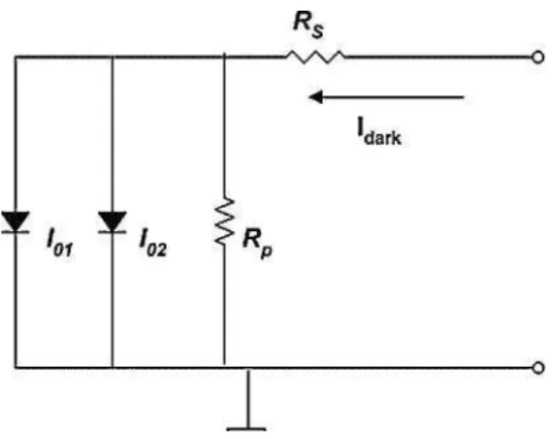
The dark behaviour of a solar cell has traditionally
been modelled by means of an equivalent circuit
consisting of a lumped series resistance (Rs), a lumped
shunt resistance (R
P) and a diode with an ideality factor
ranging from 1 to 2. In most cases, the experimental
data for III-V solar cells cannot be fitted properly using
just one diode. Consequently, a two-diode model
consisting of one diode with an ideality factor equal
to 1 (mi) and
o n ediode with an ideality factor equal to
2 (m
2) should be used whose equivalent circuit is
shown in Figure 1 and it is described by:
Nevertheless, even using two diodes, most dark I-V
curves can only be partially fitted by imposing values
for mi and m
2different from 1 and 2, respectively.
Figure 1. Two-diode lumped model for a single-junction
solar cell in dark conditions
lacks a physical meaning since classic semiconductor
theory regarding recombination mechanism in a p-n
junction assumes two different types of recombination
mechanism: the kT-recombination, that takes place in
the neutral zones and the 2kT-recombination related
to the space charge. For concentrator solar cells, the
perimeter recombination is also very relevant and
it also follows a 2kT-recombination. Consequently
when the solar cell is modelled by means of two
diodes, the ideality factors must be 1 and 2.
Additionally, the two-diode model is based on
lumped parameters and assumes that the series
resistance (R
s) and the shunt resistance (R
P) in the
dark and under illumination are the same. In other
words, in the two-diode model the lumped parameters
should result in the same ohmic losses both with and
without illumination. This simulation assumption is in
opposition to the observed behaviour in concentrator
solar cells. In fact, the resultant parameters extracted
from the dark I-V curve and the illumination data
disagree. Different strategies have been developed in
order to fit dark and illumination data under different
concentration levels. Some authors have proposed
the variation of the ideality factor which implies
different values for the inverse current saturation (7oi,
/02) while others define a R
svalue for dark conditions
and a different R
svalue for illumination
con-ditions.
But, for a real III-V solar cell, the series resistance
must be independent of the illumination level since
some components, such as the emitter sheet resistance,
are intrinsic properties of the solar cell, and others,
such as the metal sheet resistance, are a consequence of
the metallization procedure. On the other hand,
con-cerning the recombination mechanisms, GaAs solar
cells reach the high injection regime for illumination
levels at around 5000X-10 000X. Consequently, the
high injection regime is far from the actual operating
conditions of concentrator solar cells. Then, for the
viable concentration range, it can be assumed that /
0i
and /
02d
mGaAs solar cells are also independent on the
illumination level. But even though these parameters
can be considered as constants, the influence of the
series resistance components and the recombination
mechanisms on the solar cell response vary with
concentration. This is why some authors define a
different ideality factor or R
svalues depending on the
illumination level.
Consequently, a more accurate model is required in
order to provide fitting parameters that allow a proper
data fit together with a reliable prediction of the solar
cell response both in dark and under illumination
(including concentration).
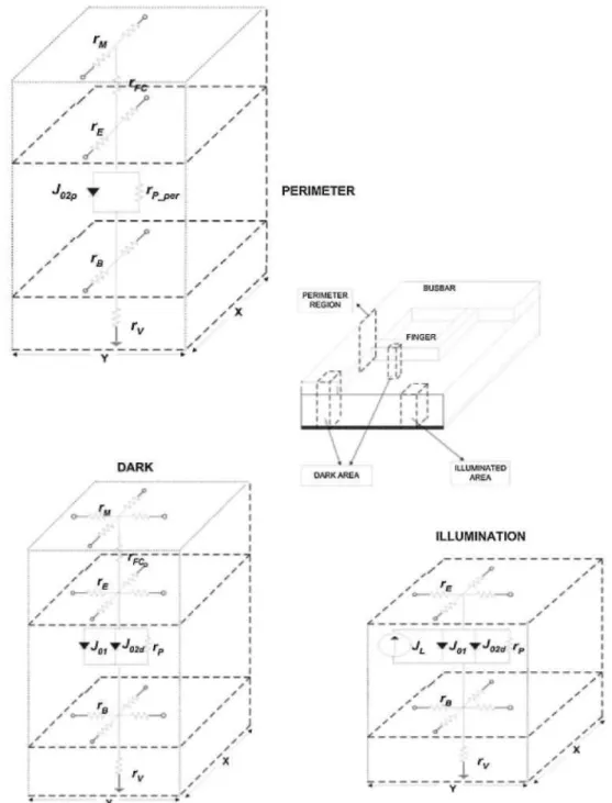
DISTRIBUTED MODEL
Accordingly, an explanation of the dark I-V curve is
presented in this paper using a 3D network model
based on distributed circuit units, that is, it does not
resolve the continuity equations in 3D, but it does
model the different current paths in a distributed
manner. The model was previously presented and
has already been successfully used for different
applications. This model looks at all the loss
effects (recombination, series resistance and shunt
resistance) in a distributed manner by dividing the
solar cell into elementary units (illumination, dark and
perimeter) and assigning a specific circuit model to
each one (Figure 2). With regard to the recombination
mechanisms, three diodes are used: one for the neutral
zone (mi = 1
a nd J01),
o n ef°
rthe depletion region
(m
2<j = 2 and /02a)
a nd
o n ef°
rthe perimeter (m
2p= 2
and /o2p)- For the ohmic losses in a single junction
solar cell, the series resistance components are: the
front contact specific resistance
(PFC),the grid metal
sheet resistance (r
Msheet), the vertical series resistance
(r
v) which results from the vertical current flow (i.e.
through the base, substrate and back contact) and the
emitter sheet resistance (r
Esheet). Concerning the shunt
resistance, two different origins are taken into account:
the shunt resistance in the bulk device (r
P) and the
Figure 2. 3D network model for a single-junction solar cell showing the main elementary units
III-V concentrator solar cells the perimeter/area ratio
is high and consequently the independent treatment of
the shunt resistance at the perimeter and in the bulk is
of great relevance for an accurate modelling. The
different circuit units used in the 3D distributed model
are presented in Figure 2 for a single junction device. It
is important to bear in mind that different circuit units
length, and the size of the illumination circuit units that must be smaller than the minority carrier diffusion length in the emitter or the base.
EXPERIMENTAL
A concentrator GaAs solar cell has been analysed by means of the 3D network model and the two-diode model for dark and concentration conditions. The semiconductor structure of the solar cell has been grown on a p-type GaAs substrate (1 x 10 cm~ ) with the following layers: a 200 nm Alo.3Gao.7As BSF (5 x 101 8cm~3), a 3.5 |Jim p-type base (2 x 101 7crrT3),
a 180 nm n-type emitter (1 x 101 8cm~3) and a 25 nm
GalnP window layer (1
contact metallization is based on AuGe/Ni/Au 1 01 8c r r r3) . The front
and the back contact metallization is AuZn/Au. The solar cell active area is 1 mm2 having an inverted square grid
of 11 fingers of 3 \xm width with a pitch of 79 |Jim. The external busbar is 100 \x,m wide.
The dark I-V curve was measured using a temperature-controlled chuck once the solar cell was encapsulated on a copper heat sink for the back and with four external connections for the front. Measure-ments under concentrated illumination were also taken on the encapsulated solar cell using a flashlamp-based system with a measuring principle similar to the one described The main feature of this system is that the tracing of an I-V curve at a given concentration requires as many flashes as points on the I-V curve.
SIMULATION RESULTS
For this solar cell, the dark I-V curve has been fitted using both the 3D network model and the lumped two-diode model. For the 3D network model, only a quarter of the solar cell has been simulated for reasons of symmetry. In terms of circuit units, all the simulations have been carried out using a finger circuit unit of l x l |jLm, an illumination circuit unit of 5 x 5 |Jim, a perimeter circuit unit of 10 |Jim and a busbar circuit unit of 10 x 10|JLm. This implies that for a quarter, the number of circuit units is around 4000.
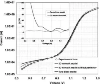
Agreement between experimental and theoretical dark I-V curve
In order to extract conclusions from the simulation results, the fit error for a fixed voltage (eF) is defined by:
where /Exp is the experimental current for a fixed
voltage and 7F r r is the fit current for the same fixed
voltage has been introduced in Figure 3.
In Figure 3, the resulting fit curves, the experimental data and the fit error are plotted. The parameters resulting from the fit are summarized in Table I. A more detailed description of the fit strategy can be found
A first conclusion that can be drawn is that by making mj equal to 1 and m2 equal to 2, the 3D model
fairly reproduces the experimental data, while the two-diode model differs at low voltages. This disagreement is because this I-V range has to be explained by means of shunt losses in the perimeter together with a bulk shunt resistance. If the perimeter effect is ignored, the 3D-network model is not able to achieve a good dark I-V curve fitting ('3D-network model without per-imeter' in Figure 3) neither.
Illumination I-V curve calculation
Once the dark I-V curve (Figure 3) has been fitted, the extracted parameters have been corroborated using them to fit illumination curves for several concen-trations with the 3D-network model and with the
two-Figure 3. Experimental dark I-V curve of a GaAs concen-trator solar cell. The thin solid black line corresponds to the data fit obtained using the 3D network model. The thick solid grey line corresponds to the data fit obtained using the 3D network model without perimeter effect. The thick solid black line corresponds to the data fit obtained using the two-diode model (Equation 1) assuming mi — 1 and m2 — 2.
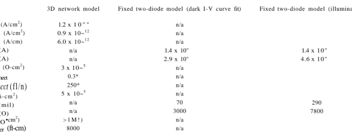
Table I. Parameters obtained from the experimental data fit of Figure 3 by the two-diode model and the 3D network model
3D network model Fixed two-diode model (dark I-V curve fit) Fixed two-diode model (illumination fit)
JQl (A/cm2)
/02d (A/cm2)
/02p (A/cm) /oi (A)
Ioi (A) Pec (O-cm2)
^Msheet
r
EShcct (fl/n)
rv(Ii-cm2) S s (mil) RP (O)
rP (O
rP_per •cm2)
(ft-cm)
1.2 x 1 0 " " 0.9 x 10~1 2
6.0 x 10~1 2
n/a n/a 3 x 10~5
0.3* 250* 5 x 10~5
n/a n/a > 1 M ! )
8000
n/a n/a n/a 1.4 x 10" 2.9 x 10" n/a n/a n/a n/a 70 3000 n/a n/a
1.4 x 10" 4.6 x 10"
290 7800
For the 3D network model only current densities (A/cm ) as well as resistance per unit area ( O c m ) are applicable since each circuit unit has its own size. All the fit parameters have been extracted from the dark I-V curve except for rMshM and rEshsst that have been obtained from the illumination data fit in Figure 5. On the other hand, when using the two-diode model, J02d and J02d are not applicable since the model does not
differentiate between the perimeter and depletion region recombination. Additionally, the parameters obtained from the illumination data fit of Figure 5 by the two-diode model are also included. Concerning the two-diode model, Rp, Rs, 70i and I02 have been obtained from the dark I-V curve fitting.
'Although Figure 6 shows that rMsheet and rEsbcl>t have no influence in the dark, these parameters have been obtained from the fit of the illumination curves,
n/a: not applicable.
diode model (Figure 4). As can be seen, the simulated efficiency for a wide range of concentrations obtained through the two-diode model using the parameters obtained from the dark I-V curve fit (Table I) is greatly overestimated for medium and high concentrations, while it is underestimated for low concentrations. This behaviour is a result of the lumped nature of the two-diode model that assumes that RP (that mainly
influences at low concentrations) and Rs (that mainly
influences at middle and high concentrations) are the same in the dark and under illumination. In order to verify this hypothesis, the illumination data of Figure 4 has been fitted by means of the two-diode model. The resulting parameters are also shown in Table I. This table shows that the values of 70i and I02 are different
depending on whether the fitting is carried out on the dark I-V curve or the illumination data. Concerning the ohmic losses, the value obtained for Rs from the illumination data fit is much higher than the value extracted from the dark I-V curve. That is, the value obtained for Rs from the fit of the dark I-V curve using
the two-diode model is only a part of the Rs detected
under illumination. On the other hand, the Rp value obtained from the illumination data fit is also higher than the value extracted from the dark I-V fit. This is because under illumination conditions the shunt resistance losses are smaller as result of many parallel current paths. This effect is also observable when the
Figure 4. Efficiency as a function of concentration. The thick grey solid line corresponds to every concentration fit by means of the 3D network model using the parameters extracted from the dark I-V curve of Figure 4 ('3D network model'). The dashed black line corresponds to every con-centration fit by means of the two-diode model using the parameters extracted from the dark I-V curve of Figure 4 ('Two-diode model with "dark" parameters'). The thick black solid line corresponds to every concentration fit by means of the two-diode model using different parameters than those obtained from the dark I-V curve fitting ('Two-diode model with "illumination" parameters'). The dashed grey line corresponds to every concentration fit by means of 3D network model neglecting the perimeter effect ('3D network model without perimeter').These parameters are
perimeter effect is ignored in the 3D network model. If
the dark I-V is fitting by the 3D model neglecting the
perimeter effect ('3D network model without
per-imeter' in Figure 3) the resultant fitting values generate
that at IX the efficiency is underestimated ('3D
network model without perimeter' in Figure 4). This is
because when the perimeter is ignored the r
pvalue
required to fit the dark I-V curve of Figure 3 is much
lower (r
p= 7500 il-cm
2) than when the perimeter is
considered ( r
p> l Mil-cm ).
In contrast, the values of the series and shunt
resistance components resulting from the dark I-V fit
with the 3D network model allow an accurate
descrip-tion of the illuminated I-V curve, since this model
allows alternative current paths through different
resistances in parallel (see Figure 2) as actually
happens in a real solar cell.
DISCUSSION
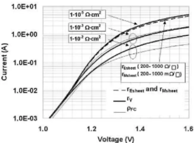
Figure 5. Simulated dark I-V curves obtained through the
3D network model with r
vvarying from 1 x 1CF to
1 x l(T
2n-cm
2and p?
cfrom 1 x 1(T
5to 1 x 10~
2fl-cm
2Additionally, the simulation for f
Esheetequal to 200 and
1000 fl/n and for r
Msheetequal to 200 and lOOOmfl/D
has been included (dashed black line)
In order to quantify the influence of the different series
resistance components under dark conditions, the dark
I-V curve has been simulated by the 3D network
model varying different series resistance components
(
rEsheet from 200 to 1000 VLl •, r
Msheetfrom 200
to 1000mn/rj, ppc and r
vfrom 1 x 10~
5to
1 x 10~ fl-cm ) for a concentrator solar cell. In these
cases, the influence of a given series resistance
component has been obtained by fixing the other
three series resistance components to their typical
values for the state of the art of the technology (r
Esheet=
200 n / D , r
Msheet= 0.2fl/n, PFC = 5X 1 0
- 5fl-cm
2and r
v= 5 x 10~
5fl-cm
2). The first conclusion
obtain-ed from Figure 5 is that both the emitter sheet
resistance (r
Esheet) and the metal sheet resistance
(
rMsheet) have a negligible impact on the resulting dark
I-V curves since, for any value, the resultant I-V curve
is equivalent (dashed line in Figure 5). On the other
hand, both the vertical resistance (r
v) and the front grid
specific contact resistance (ppc) show a big influence
under dark conditions. This effect is only visible by
using a distributed model.
This conclusion implies that the dark I-V curve is of
special relevance in detecting ohmic losses related to
the vertical current flow (semiconductor structure,
substrate and back contact and the front metal specific
resistance), but no effect derived from the lateral
current flow such as through the emitter or the metal
sheet resistance is detected, although their influence
under concentrated illumination is very important.
Consequently, a concentrator solar cell could show a
low series resistance in the dark but a very high ohmic
losses under concentration, for example as a result of a
high metal sheet resistance or emitter sheet resistance.
Additionally, the 3D network model allows the
simulation of the voltage distribution on the solar
cell surface. In Figure 6, a false greyscale map of
the simulated voltage distribution of a GaAs single
junction concentrator solar cell forward biased at 1.3 V
is presented. The voltage and current density through
the vertical resistance, r
v, of a cross section in the
centre of the cell (white line) has been included in the
Figure 6.
From Figure 6, it can be derived that the maximum
voltage drop between the centre of the active area and
the busbar region where the external wires are placed
(each corner) is around 0.1 V (1.3V at the busbar
and 1.2 V at the centre of the cell). In terms of current,
this voltage drop means that the current flowing
through the active area region is about one order of
magnitude lower than the one through the external
busbar (Figure 6). In fact, according to the
exper-imental data of Figure 3 (dark I-V curve), the
corresponding current for 1.3 V is 1 A. For a GaAs
solar cell of 1.2 x 1.2 mm, the current density for 1.3 V
is 69 A/cm
2. This reference value has been included in
Figure 6. False grey scale map of the simulated voltage distribution under dark configuration for a bias polarization of 1.3 V at the four corners. Additionally, the voltage and density current has been calculated in a transversal section
(white line in the greyscale map)
mainly vertical beneath the busbar and, consequently, only ry and p^c have influence, thus explaining the results discussed above. As a rule of thumb, the dark I-V curve only characterizes the solar cell portion beneath the busbar or metallization path where the external connections are placed for concentrator solar cell with a grid orientated for a point focus concentrator.
solar cell could be fairly fitted by the two-diode model (equation 1), the extracted parameters are not compatible with the experimental data under illumina-tion. But, by using a 3D network model, both the dark and the illumination data can be fitted with the same set of fitting parameters without any correction factor, being the first time that a good experimental fitting for dark and concentrated illumination data can be achieved with the same set of parameters.
In second place, the origin of the differences between the dark and illumination ohmic losses have also been presented, showing that the most important series resistance components for the dark I-V curve are those related to the vertical current flow such as, the vertical resistance ( rv) and the front contact-specific
resistance (ppc), while the emitter sheet resistance (rEsheet) a nd the metal sheet resistance (rM s h e e t) have no
influence on the dark I-V measurements, but they have a key role under concentrated illumination. This result is of special relevance to understand and extract reliable information from the dark I-V curve.
Finally, a voltage distribution in the dark is presented together with a density current in a transversal section of a GaAs solar cell, concluding that in a dark I-V measurement the current flowing through the active area region is about one order of magnitude lower than the one through the external busbar. This result reinforces the previous conclusion that only ry and ppc have influence in the dark I-V measurements.
Acknowledgements
This paper has been supported by the European Commission under contract SES6-CT-2003-502620 (FULLSPECTRUM project). The Spanish Ministerio de Educacion y Ciencia has also contributed with the CONSOLIDER-INGENIO 2010 programme by means of the GENESIS FV project and also with the research projects with references TEC2005-02745 and TEC2004-22300-E as well as the Comu-nidad de Madrid under NUMANCIA programme (S-505/ENE/0310). The authors would like to thank the reviewers their interesting comments and suggestions.
CONCLUSIONS
The main conclusions of this paper are, in first place, that even though the dark I-V curve of a concentrator
REFERENCES
Photovoltaics: Research and Applications 2003; 11(3):
165-178.
Vishnoi A, Gopal R, Dwivedi R, Srivastava SK. Dis-tributed parameter analysis of dark I-V characteristics of the solar cell: estimation of equivalent lumped series resistance and diode quality factor. Proceedings G IEEE
of Circuits, Devices and Systems 1993; 140(3): 155-164.
Algora C, Marti A, Araiijo GL. Characterization of the dark I-V curve of p/n GaAs heteroface solar cells.
Proceeding of the 8th photovoltaic solar energy con-ference, 1988; 1512-1516.
Kaminski A, Marchand JJ, Fave A, Laugier A. New method of parameters extraction from dark I-V curve.
IEEE Photovoltaic Specialists Conference 1997; 1:
203-206.
Haouari-Merbah M, Belhamel M, Tobias I, Ruiz JM. Method of extraction and analysis of solar cell parameters from the dark current-voltage curve. Spanish
Conference on Electron Devices 2005; 2: 275-277.
Grove AS. Physics and Technology of Semiconductor
Devices, Ed. John Wiley and Sons, 1967.
Henry CH, Logan RA, Merrit FR. The effect of surface recombination on current in AlxGa^xAs heterojunctions.
Journal of Applied Physics 1978; 49(6): 3530-3542.
Araki K, Yamaguchi M. Extended distributed model for analysis of non-ideal concentrator operation. Solar
Energy Materials and Solar Cell 2003; 75: 467^173.
Nielsen LD. Distributed series resistance effects in solar cells. IEEE Transactions on Electron Devices 1982;
ED-29: 821-827.
Aberle AG, Wenham SR, Green MA. A new method for accurate measurements of the lumped series resistance of solar cells. IEEE Photovoltaic Specialists Conference 1993; 133-139. DOI: 10.1109/PVSC.1993.347065
Araujo GL, Cuevas A, Ruiz JM. The effect of distributed series resistance on the dark and illuminated current— voltage characteristics of solar cells. IEEE Transactions
on Electron Devices 1986; 33(3): 3 9 1 ^ 0 1 .
The voltage that needs to be applied to a pn+ junction in
order to reach the high injection regime (VHi) is Vm — 2 Y m (-f4) > where NA is the doping level of the p side
and nt is the intrinsic concentration of the semiconductor
[GL: Araujo, G. Sala, J.M. Ruiz, "Fisica de los dis-positivitos electronicos", ETSIT, 1980, ISBN: 84-7402-1002-2]. For a typical GaAs concentrator solar cell, NA is between 2-10 and 1-10 cm~ thus obtain-ing 1.281 V < VHI < 1.361 V Taking into account that VH! is the voltage applied at the pn junction (so ohmic losses must be considered), illumination concentrations between 5000X and 1000X are required.
Galiana B, Algora C, Rey-Stolle I, Vara IG. A 3-D model for concentrator solar cells based on distributed circuit units. IEEE Transactions on Electron Devices 2005; 52(12): 2552-2558.
Gonzalez JR, Rey-Stolle I, Algora C, Galiana B. Micro-plasma breakdown in high-concentration III-V solar cells. IEEE Electron Device Letters 2005; 26(12): 867-869.
Galiana B, Rey-Stolle I, Algora C. Comparison of ID and 3D analysis of the front contact influence on GaAs concentrator solar cell performance. Solar Energy
Materials and Solar Cells 2006; 90(16):
2589-2604.
Williams RE. Modern GaAs processing methods. Artech House, Boston-EE.UU, 1990.
Keogh W, Cuevas A. Simple Flashlam pTesting of Solar Cells. Proceedings of the 26th IEEE Photovoltaic