Optical properties and microstructure of 2.02-3.30 eV ZnCdO nanowires:
Effect of thermal annealing
M. Lopez-Ponce, A. Hierro, J. M. Ulloa, P. Lefebvre, E. Muñoz et al.
Citation: Appl. Phys. Lett. 102, 143103 (2013); doi: 10.1063/1.4799491
View online: http://dx.doi.org/10.1063/1.4799491
View Table of Contents: http://apl.aip.org/resource/1/APPLAB/v102/i14
Published by the American Institute of Physics.
Additional information on Appl. Phys. Lett.
Journal Homepage: http://apl.aip.org/
Journal Information: http://apl.aip.org/about/about_the_journal
Top downloads: http://apl.aip.org/features/most_downloaded
Optical properties and microstructure of 2.02-3.30 eV ZnCdO nanowires:
Effect of thermal annealing
M. Lopez-Ponce,1A. Hierro,1,a)J. M. Ulloa,1P. Lefebvre,1,b)E. Mu~noz,1S. Agouram,2 V. Munoz-Sanjos~ e,2K. Yamamoto,3A. Nakamura,3and J. Temmyo3
1
ISOM and Dept. Ing. Electronica, Univ. Politecnica Madrid, Avda. Complutense 30, 28040 Madrid, Spain
2
Department of Applied Physics and Electromagnetism, University Valencia, C/Dr. Moliner 50, 46100 Burjassot, Spain
3
Research Institute of Electronics, Shizuoka University, 3-5-1 Johoku, Hamamatsu 432-8011, Japan
(Received 16 November 2012; accepted 20 March 2013; published online 8 April 2013)
ZnCdO nanowires with up to 45% Cd are demonstrated showing room temperature photoluminescence (PL) down to 2.02 eV and a radiative efficiency similar to that of ZnO nanowires. Analysis of the microstructure in individual nanowires confirms the presence of a single wurtzite phase even at the highest Cd contents, with a homogeneous distribution of Cd both in the longitudinal and transverse directions. Thermal annealing at 550C yields an overall improvement of the PL, which is blue-shifted as a result of the homogeneous decrease of Cd throughout the nanowire, but the single wurtzite structure is fully maintained. VC 2013 American Institute of Physics. [http://dx.doi.org/10.1063/1.4799491]
The development of ZnO-based electronic and optoelec-tronic devices, both in thin films and nanostructures, has reached a point where using heterostructures has become necessary in order to tune the bandgap and thus control the injection and confinement of charge carriers. Indeed, by alloying with Mg or Cd, the ZnO bandgap (3.37 eV) can be theoretically changed from 7.8 eV (MgO) to 2.3 eV (CdO).1,2However, in contrast to ZnO, which shows a wurt-zite structure, CdO and MgO naturally show a rocksalt struc-ture, and thus 7.8 and 2.3 eV correspond to the direct bandgap of the rocksalt phases of MgO and CdO, respec-tively. This transition from wurtzite to rock-salt leads to phase separation in the alloys, limiting the maximum amount of Cd or Mg that can be incorporated into ZnO.3,4In the par-ticular case of Cd, the high vapour pressure and low thermo-dynamic solid solubility (2%) pose an additional problem for the realization of ZnCdO layers with high Cd contents. Although thin films with Cd contents up to 69.7% have been demonstrated with wurtzite structure using remote-plasma-enhanced metal-organic chemical vapour deposition (RPE-MOCVD),5most published reports do not reach higher Cd contents than 10%–15%, probably as a result of this phase separation problem.6Besides, the fabrication of a de-vice using these alloys adds an additional problem: the post-growth thermal budget resulting from ohmic contact anneal-ing, dopant activation, or point defect reduction, through thermal annealing. Indeed, several groups have reported the use of thermal annealing in the 500–800C range to decrease the ohmic contact resistance to ZnO,7whereas others have used annealing as high as 850–900C to increase the carrier mobility8or to activate p-type dopants.9Because of the low growth temperatures used for ZnCdO, which are in the 300–500C range,10,11 these post growth annealing proc-esses are likely to induce structural, electrical, and optical
changes in the alloys. These changes need to be accounted for and understood, especially for the case of ZnCdO, since Cd has a strong tendency to diffuse.12
In the present study, we have used a combination of photoluminescence (PL), high resolution x-ray diffraction (HRXRD), high resolution transmission electron microscopy (HRTEM), and micro energy dispersive x-ray spectroscopy (micro-EDX) to quantitatively analyze the incorporation of Cd in ZnCdO nanowires with wurtzite structure, as well as the impact that post-growth thermal annealing has on their microstructure and radiative efficiency.
Vertically aligned c-axis ZnCdO nanowires were grown at 300C on a-plane sapphire substrates by RPE-MOCVD. Details on the growth can be found in Ref. 13. A series of four samples with nominal Cd concentrations ranging from x¼0 to 0.45 were studied. The nanowires were typically 1–3lm-long and 100–200 nm-wide. A representative plan and cross sectional view of the nanowires are shown in Fig.
1. This set of samples was exposed to a rapid thermal anneal-ing (RTA) cycle in a N2atmosphere with temperatures
rang-ing from 250 to 550C for varying times. Continuous-wave PL spectroscopy at room temperature and under vacuum conditions was done in backscattering configuration by using a He–Cd laser (k¼325 nm) under constant power density excitation. The crystal microstructure and Cd concentration profiles of the self-aligned nanowires were assessed by HRXRD scans around the [0001] reflections using an X’Pert PRO PANalytical diffractometer. HRTEM and micro-EDX were performed on individual nanowires using a field-emission TECNAI G2F20 microscope (from FEI) operated at 200 kV. In order to avoid any possible influence of the sample inhomogeneity on the analysis, both the optical and structural characterizations were performed in the same sam-ple piece before and after annealing.
As shown in Figures 2 and 3, the room temperature near-band-edge PL energy red-shifts with increasing Cd con-tent down to 2.02 eV, for 45% Cd, covering a large part of the visible spectrum. The fact that a lower emission energy
a)Electronic mail: [email protected]
b)Now at Laboratoire Charles Coulomb, CNRS, Universite Montpellier 2,
Montpellier, France.
than the bandgap of CdO is obtained is likely the result of the large Stokes shifts present in this alloy.13 Even though the PL full width at half maximum (FWHM) increases when adding Cd to ZnO, it is worth noticing that the PL peak in-tensity at room temperature is not strongly affected by the Cd content. Indeed, the PL intensity in the ZnCdO nanowires is quite similar to that of the ZnO nanowires even for emis-sion energies as low as 2.02 eV (Fig. 2). The increase in FWHM as Cd is added to ZnO is the well-known effect of exciton localization on potential fluctuations induced by nat-ural alloy disorder.13,14 Indeed, Buyanova et al.14 showed that this was the case for ZnCdO samples with 9% and 15.7% Cd and proposed that increasing the Cd content leads to a decrease of the exciton binding energy and, therefore, to an increase of the Bohr radius. The latter can then lead to a larger tunnelling probability between the band tail states, thus leading to a larger PL FWHM in ZnCdO versus ZnO. The Stokes shift observed by Buyanovaet al. was constant in the 9%–15.7% Cd range. In contrast, we observe that the FWHM not only increases from ZnO to ZnCdO but actually depends on Cd and shows a maximum value for20% Cd. In fact, Yamamotoet al.13showed that in ZnCdO films, the effect of alloy disorder is maximum for Cd concentrations around 20%–30%, leading to a maximum in the Stokes shift and PL FWHM, alike the behaviour here observed. Thus, we can conclude that the presence of Cd induces a larger PL
FWHM likely as a result of both localization potential (induced by alloy disorder) and increased Bohr radius.
Choosing the sample with the intermediate 27% Cd con-tent as a representative sample of the series, we can observe in Fig. 3(b)the effect that the RTA temperature has on the PL. The RTA time was also varied from 1 to 5 min—not shown—and it was found that the entire enhancement in PL intensity takes place during the first minute, reason why this cycle time was used for the rest of the study. The peak energy exhibits a significant blue shift only for the largest annealing temperature, i.e., 550C, while the PL intensity is actually enhanced as soon as the growth temperature (300C) is exceeded. The improvement in PL intensity for the intermediate annealing temperatures, i.e., 400 and 500C, is likely linked to the reduction of non-radiative channels via the decrease in concentration of the most com-mon point defects found in ZnO, which for highly n-type material like in our case, are Zn vacancies (VZn) and/or
com-plexes involving this type of point defects.15,16 For these annealing temperatures (400–500C), there is only a small blue shift, and thus the targeted PL emission energy is mostly maintained but with enhanced radiative emission. Hence, the 400–500C range seems appropriate for anneal-ing ohmic contacts on ZnCdO. At 550C, there is already a sizeable PL blue-shift as well as a large reduction of the PL FWHM. Since this temperature is also close to the upper limit typically used for ohmic contact annealing in this type of oxides, it was chosen for the quantitative analysis of the Cd concentration profiles and microstructure after annealing. The aforementioned enhancement of the PL intensity upon annealing is larger in the reference ZnO sample than in the Cd-containing ones, and in fact the 27% Cd sample shows the lowest enhancement (Fig.3(a)). This effect can be explained to result from the stronger localization of the exci-ton when Cd is present, especially for the 27% Cd sample, where the effect of alloy disorder is maximum.13Under these
FIG. 2. Room temperature photoluminescence spectra of the as-grown and annealed ZnCdO nanowires for different Cd contents, as indicated.
FIG. 3. (a) Dependence on Cd content of the RT-PL peak energy, intensity and FWHM, both for the as-grown and annealed nanowires. (b) Dependence on annealing temperature of the PL properties for the Zn0.73Cd0.27O
nano-wires. The annealing time was 1 min. Connecting lines are a guide to the eye. FIG. 1. Plan view (a) and cross-sectional view (b) SEM images of the
as-grown Zn0.73Cd0.27O nanowires.
strong localization conditions, the exciton is less sensitive to the reduction of non-radiative recombination paths upon annealing, and thus the radiative emission is only lightly affected. The stronger reduction of the PL FWHM in the samples with 14% and 27% Cd is likely related to decreasing the degree of alloy disorder after annealing. Annealing also induces a PL blue shift that increases with the Cd content, reaching 170 meV for the nanowires with 45% Cd, and whose origin is discussed below in terms of the nanowire microstructure.
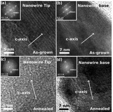
As mentioned in the introduction, increasing the Cd con-tent in ZnCdO above 15%–20% typically leads to phase sep-aration and a mixed wurtzite/rock-salt phase appears.3This effect has traditionally limited the spectrum energies that can be covered with ZnCdO to values not far from that of the ZnO bandgap. This limitation is even more pronounced when this ternary alloy is exposed to a thermal annealing cycle, especially at high temperatures, where the diffusion of Cd is enhanced allowing the formation of the rocksalt phase. So, as a first step, the Cd content of the as-grown nanowires was measured by EDX. To do so, the nanowires were removed from the substrate and deposited on a TEM grid. The mean Cd content was then obtained for each sample by analyzing the EDX signal from ensembles of tens of nano-wires (by defocusing the microscope spot to include the sig-nal from many nanowires), thus averaging out possible inhomogeneities in the Cd profile within the nanowire as well as among different nanowires. The resulting measured Cd content is shown in the x-axis of Fig. 6(b) and has an error bar of62.5%, mostly given by the EDX concentration resolution (2%). As shown in Fig.6, the measured Cd con-centrations matched well the nominal ones for all samples. In addition, HRTEM analysis of as-grown single nanowires only shows the presence of the wurtzite crystal structure, even for the nanowires with 45% Cd, contrary to what is typ-ically reported in the literature. Figs. 4(a) and 4(b) show
typical HRTEM images and diffraction patterns of the nano-wire tip and base for the intermediate 27% Cd sample, as a representative example. No trace of crystal phase separation is observed. An analysis of the crystal plane separation through the fast Fourier transform (FFT) of the diffraction pattern does show a reduction of the lattice parameter closer to the surface, base, and tip of the nanowires, indicating a reduction of Cd content in these regions, consistent with its low vapour pressure and the difficulty to incorporate it in the lattice. However, the rock-salt phase is not observed even for 45% Cd contents.
To confirm the Cd concentration profile within the nano-wire, micro-EDX was performed along the longitudinal and transverse axes of individual nanowires of each sample. The performed microanalysis has a spatial resolution of 2 nm and a concentration resolution of 2%. Figure 5(a) shows the Cd and Zn profiles for the as-grown 27% Cd sample, where we can observe that the Cd distribution is homogene-ous along the nanowire. Also, across the nanowire, the Cd content decreases closer to the surface, in agreement with what was observed by HRTEM in the measurement of the atomic plane separation. The fact that the Cd and Zn concen-tration profiles are anticorrelated and add up to be one is a good indication that this result is not a measurement artefact. In addition, Cd is not observed to accumulate in any specific regions, even for the highest Cd content of 45%. Similar results were obtained for all Cd-containing samples.
Analyzing the annealed nanowires by HRTEM, it is observed that the wurtzite microstructure is completely main-tained (Figs.4(c)and4(d)), and no traces of the rocksalt crys-tal structure are observed, regardless of the Cd content. What micro-EDX indeed shows (Fig.5(b)) is that the homogeneous distribution of Cd along and across the nanowire remains after annealing, and the same Cd deficiency as in the as-grown nanowires is observed closer to the nanowire surface. The
FIG. 4. HRTEM images of two Zn0.73Cd0.27O nanowires, (a), (b) as-grown,
and (c), (d) annealed. The insets show the FFT of the diffraction pattern.
FIG. 5. Cd and Zn concentration profiles of two individual Zn0.73Cd0.27O
similar Cd contents observed in Fig.5between the as-grown and annealed nanowires are the result of the large error bar in the EDX measurement, which masks this variation. In fact, and as mentioned before, the changes in the Cd concentration between as-grown and annealed nanowires are only observ-able when the signal from ensembles of tens of nanowires is measured, yielding the results shown in Fig.6(b). The general reduction of the Cd content taking place during annealing can be explained to result from out-diffusion to the surface of this element followed by evaporation. Indeed, Azarov et al.17 showed that upon annealing at high temperatures, ZnCdO films with 7% Cd also show a significant evaporation of Cd through the surface and that above 600C, the diffusion of Cd already begins. In the case of nanowires, where the surface/ volume ratio is large, the Cd atoms have to diffuse a short dis-tance to be able to evaporate, reason why such a pronounced effect is already observed at 550C.
The change in lattice parameter of the nanowires upon annealing was also confirmed with HRXRD of the vertically aligned nanowires. Figure6(a)shows a representative exam-ple of the diffraction pattern along the (0001) direction, and it can clearly be observed how the ZnCdO-related peak shifts upon annealing as a result of the change of the c-axis lattice parameter, again indicative of the reduction of Cd in the annealed nanowires. The resulting c-axis lattice parameters of all samples as a function of the EDX-measured Cd content are shown in Fig.6(b). A quadratic fit to the data, including both as-grown and annealed nanowires, yields the relation c(nm)¼0.520þ0.064x0.044x2, quite similar to previous references in as-grown thin films (Refs. 13 and 18). Therefore, the c-axis is univocally determined by the Cd content, regardless of the exposure of the nanowires to
thermal annealing. In addition, by plotting the measured PL peak energy as a function of the measured Cd content, we see a good match for both as-grown and annealed samples. Using also a quadratic fit to the experimental data, the evolu-tion of the ZnxCd1-xO near band edge emission follows the
expression E(eV)¼3.306.26 xþ7.56x2(0x0.45). Thus, the blue-shift of the PL energy upon annealing can be univocally assigned to an overall reduction of Cd content in the nanowire while maintaining the wurtzite structure.
In order to relate the PL energy to the Cd content within the nanowire, one needs to account for several effects. In ZnO nanowires, a charge depletion region exists at the sur-face19confining the carriers within the nanowire core. This effect is likely reduced in ZnCdO since the residual n-type concentration is typically larger than in ZnO, and so the surface-related depletion region should be thinner. However, as we showed above, there is a Cd depletion close to the sur-face both in as-grown and annealed nanowires, effect that would create an additional potential barrier that further con-fines the carriers within the nanowire. Thus, the PL emission energy has to be linked to the measured Cd content within the core of the nanowire.
In conclusion, we have demonstrated ZnCdO nanowires with room temperature PL energies covering the spectral region from 3.3 eV down to 2.02 eV, corresponding to a measured Cd concentration in the nanowire from 0% to 45%. Moreover, all nanowires show a wurtzite structure with no indication of crystal phase separation or Cd accumulation. These nanowires have radiative efficiencies that compare well to that of the reference ZnO nanowires. Even though the growth temperature is quite low in these nanowires (300C), thermal annealing up to 550C may be used in future device processing. Indeed, after a 550C annealing, the single wurtzite structure is completely maintained even with 45% Cd, and the only detrimental effect is the PL blue shift that arises from a homogeneous reduction of Cd along and across the nanowire, which is lost through evaporation.
The authors would like to thank T. Brazzini for assistance with the XRD measurements and gratefully acknowledge the support of the Ministry of Economy and Competitiveness (MINECO) and the EU (FEDER) through Project No. TEC2011-28076-C02-01/02, the MINECO-Japanese Science and Technology Agency (JST) Project No. PIB2010JP-00279, the Generalitat Valenciana under Project Nos. Prometeo/2011-035 and ISIC/2012/008, and the Institute of Nanotechnologies for Clean Energies of the Generalitat Valenciana.
1K. Takahashi, A. Yoshikawa, and A. Sandhu, Wide Bandgap
Semiconductors: Fundamental Properties and Modern Photonic and Electronic Devices(Springer, 2007).
2F. P. Koffyberg,Phys. Rev. B13, 4470 (1976).
3K. Sakurai, T. Takagi, T. Kubo, D. Kajita, T. Tanabe, H. Takasu, Sz.
Fujita, and Sg. Fujita, J. Cryst. Growth514, 237 (2002).
4
W. I. Park, G.-C. Yi, and H. M. Jang,Appl. Phys. Lett.79, 2022 (2001).
5S. Shigemori, A. Nakamura, J. Ishihara, T. Aoki, and J. Temmyo,Jpn. J.
Appl. Phys., Part 243, L1088 (2004).
6
F. Bertram, S. Giemsch, D. Forster, J. Christen, R. Kling, C. Kirchner, and A. Waag,Appl. Phys. Lett.88, 061915 (2006).
7L. J. Mandalapu, Z. Yang, and J. L. Liu,Appl. Phys. Lett.90, 252103 (2007). 8K. K. Kim, S. Niki, J. Y. Oh, J. O. Song, T. Y. Seong, S. J. Park, S. Fujita,
and S. W. Kim,J. Appl. Phys.97, 066103 (2005). FIG. 6. (a) HRXRD diffraction pattern for the as-grown and annealed
Zn0.55Cd0.45O nanowires. (b) Dependence of the c-axis lattice parameter
(extracted from HRXRD) and PL energy, on the Cd content determined by EDX on both as-grown (solid symbols) and annealed (hollow symbols) sam-ples. Note that for x¼0 (pure ZnO), the measured PL energy and c-axis lat-tice parameter were identical for the as-grown and annealed samples. The solid lines are quadratic fits to the experimental data.
9C. C. Lin, C. Y. Chen, S. Y. Cheng, S. Y. Cheng, and H. Y. Lee,Appl.
Phys. Lett.84, 5040 (2004).
10
J. Ishihara, A. Nakamura, S. Shigemori, T. Aoki, and J. Temmyo,Appl. Phys. Lett.89, 091914 (2006).
11T. Ohashi, K. Yamamoto, A. Nakamura, and J. Temmyo,Jpn. J. Appl.
Phys., Part 147, 2961 (2008).
12
A. V. Thompson, C. Boutwell, J. W. Mares, W. V. Schoenfeld, A. Osinsky, B. Hertog, J. Q. Xie, S. J. Pearton, and D. P. Norton,Appl. Phys. Lett.91, 201921 (2007).
13
K. Yamamoto, T. Tsuboi, T. Ohashi, T. Tawara, H. Gotoh, A. Nakamura, and J. Temmyo,J. Cryst. Growth312, 1703 (2010).
14I. A. Buyanova, J. P. Bergman, G. Pozina, W. M. Chen, S. Rawal, D. P.
Norton, S. J. Pearton, A. Osinsky, and J. W. Dong,Appl. Phys. Lett.90, 261907 (2007).
15T. M. Børseth, B. G. Svensson, A. I. Kuznetsov, P. Klason, Q. X. Zhao,
and M. Willander,Appl. Phys. Lett.89, 262112 (2006).
16
A. Janotti and C. G. Van de Walle,Rep. Prog. Phys.72, 126501 (2009).
17
A. Y. Azarov, T. C. Zhang, B. G. Svensson, and A. Y. Kuznetsov,Appl. Phys. Lett.99, 111903 (2011).
18
T. Makino, Y. Segawa, M. Kawasaki, A. Ohtomo, R. Shiroki, K. Tamura, T. Yasuda, and H. Koinuma,Appl. Phys. Lett.78, 1237 (2001).
19