Optimum high temperature strength of two-dimensional
nanocomposites
M. A. Moncl ´us,1S. J. Zheng,2J. R. Mayeur,2I. J. Beyerlein,2N. A. Mara,2 T. Polcar,3J. Llorca,1,4and J. M. Molina-Aldaregu´ıa1,a
1IMDEA Materials Institute, C/Eric Kandel 2, 28906 Getafe, Madrid, Spain 2Los Alamos National Laboratory, Los Alamos, New Mexico 87545, USA 3Czech Technical University in Prague, Technick´a 2, Prague 6, Czech Republic
4Department of Materials Science, Polytechnic University of Madrid, E. T. S. de Ingenieros de Caminos, 28040 Madrid, Spain
(Received 30 August 2013; accepted 22 October 2013; published online 7 November 2013)
High-temperature nanoindentation was used to reveal nano-layer size effects on the hardness of two-dimensional metallic nanocomposites. We report the existence of a critical layer thickness at which strength achieves optimal thermal stability. Transmission electron microscopy and theoretical bicrystal calculations show that this optimum arises due to a transition from thermally activated glide within the layers to dislocation transmission across the layers. We demonstrate experimentally that the atomic-scale properties of the interfaces profoundly affect this critical transition. The strong implications are that interfaces can be tuned to achieve an optimum in high temperature strength in layered nanocomposite structures. © 2013 Author(s). All article content, except where otherwise noted, is licensed under a Creative Commons
Attribution 3.0 Unported License.[http://dx.doi.org/10.1063/1.4828757]
For increased energy efficiency in many future applications, there is an outstanding need for robust materials that sustain their strength at high temperatures.1,2 In this regard, nanocomposite
metallic multilayers (NMMs) are garnering much interest as promising candidates for materials in extreme conditions. NMMs are 2D nanostructured thin films or sheets that contain alternating layers of dissimilar metals with individual thicknesses far below 100 nm.3,4 Consequently, NMMs are
comprised of an unusually high density of bimetal interfaces. Experiments have shown that these interface-rich composites are several times stronger and structurally more stable after exposure to high-temperature and/or radiation environments than their constituents.4–9
The high temperature strength of the NMMs, however, has not been quantified. Current strate-gies for understanding the influence of temperature on NMM performance typically involve room temperature tests on NMMs that have been previously exposed to elevated temperatures.6,7,10,11 With the recent progress in the development of the high-temperature nanoindentation (HT-Nano) testing technique,12–16 it is now possible to study the deformation mechanisms within a localized
region of the material at high temperatures, and this capability has been shown very valuable to study two-dimensional nanocomposites.17,18
In this work, we combine the HT-Nano technique and crystal plasticity theory to study the effect of interface structure and layer thickness,L, on the high temperature behavior of a model NMM. We discover that a critical layer thickness,Lcrit, exists at which the reduction in hardness
due to temperature is minimal. We propose thatLcritcorresponds to the layer thickness at which the
dislocation mechanism transitions from intralayer slip to interface crossing. The results suggest that the latter mechanism leads to much larger reduction in hardness with temperature. With this critical insight, the possibility of tuning interfaces and their spacing within NMMs to optimize performance at high temperature becomes attainable.
aAuthor to whom correspondence should be addressed. Electronic mail:[email protected]
052103-2 Moncl ´uset al. APL Mater.1, 052103 (2013)
Recently, a few experimental and numerical studies have provided clues that the behavior of NMMs is sensitive to the structure of these interfaces,19–22which suggests that there is a potential for
tuning material properties via interface design. With this in mind, we further explore the influence of interface structure by carrying out HT-Nano testing on two NMMs with different processing histories: physical vapor deposited (PVD) Cu–Nb thin films and accumulative roll bonded (ARB) Cu–Nb sheets. More details on material fabrication can be found in the supplementary material.23Extensive
experimental work has shown that these two Cu/Nb NMMs have significantly different interface structures. The preferred interface character in the PVD foils is the classical Kurdjumov Sachs (KS) {111}<110>Cu{110}<111>Nb interface, whereas in the ARB NMMs the predominant interface character is {112}<111>Cu{112}<110>Nb.24,25 Both high resolution transmission
electron microscopy (HR-TEM) and atomic-scale calculations report that the PVD (KS) interface is atomically flat, while the ARB interface is atomically faceted.20
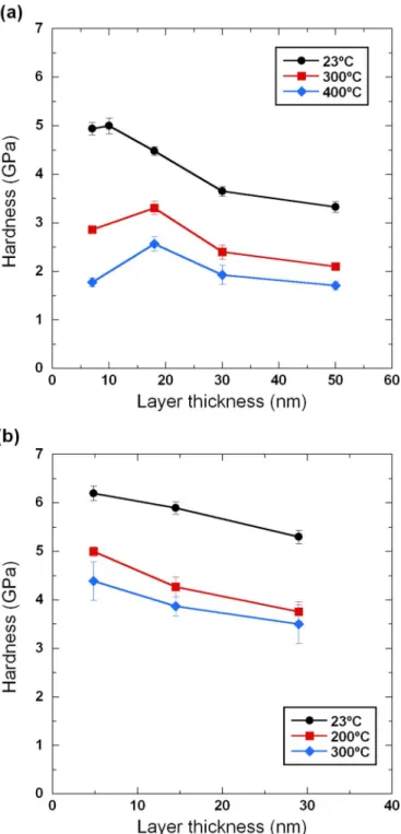
Nanoindentation measurements were performed using a Nanotest Platform 3 Instrument (Micromaterials, Wrexham, UK) fitted with a diamond Berkovich tip. The tests were carried out in inert atmosphere to minimize surface oxidation, and both the sample and indenter tip were heated independently to ensure thermal equilibrium conditions. More details on the HT-Nano testing can be found in the supplementary material.23The mean and standard deviations in hardness of the ARB
and PVD Cu–Nb NMMs are plotted in Fig.1, as a function of layer thickness,L, and temperature. For both Cu–Nb NMMs, the room temperature hardness increases or saturates with decreasingL. We find that the strengthening behavior seen in Fig.1 differs from that of single-phase Cu-based nanomaterials. In nanocrystalline Cu, a reduction in strength (softening) is observed for grain sizes of 10 nm and below.26In nanotwinned Cu, strength softening is reported for twin spacings on average
15 nm and below.27
The high temperature testing reveals some interesting differences between the PVD and ARB NMMs. First, PVD NMMs are consistently harder than the ARB NMMs at all temperatures. This result is in agreement with the trends observed in recent room temperature studies on Cu–Nb NMMs.5
Second, the room temperature hardness saturates and the high temperature hardness decreases at
L=7 nm for the ARB Cu–Nb NMM. By contrast, the strength continues to increase with decreasing layer thickness for all temperatures in the PVD Cu–Nb NMM, even for the smallest layer thickness ofL=5 nm. It has been suggested4,28 that the plateau or softening signifies the predominance of dislocation glide across interfaces over dislocation glide within individual layers. The mechanism of interface crossing is thermally activated and in principle would be enhanced by elevated temperatures. The results in Fig.1are the first indirect experimental evidence that the interfaces in the ARB NMMs are easier for dislocations to cross than those in the PVD NMMs.
It is desirable that nanomaterials strengthen as much as possible with decreasingL, exhibiting a positive and strong size effect (corresponding to the slope of the strength versus layer thickness curve). Interestingly, the size effect in the PVD foils was enhanced by deforming at higher temper-atures over the entire layer thickness range (5–30 nm) studied. Similar results were found in ARB NMMs for layer thicknesses above 18 nm. This is the first report of a strength-related size effect that can be enhanced with increasing temperature.
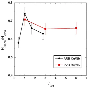
Even more remarkable is the apparent existence of a critical layer thicknessLcritat which the
reduction in hardness with temperature achieves a minimum. In the case of the ARB NMMs,Lcrit
is around 18 nm. We observe a softening in the ARB material for layer thicknesses below 18 nm. For the PVD material it is apparent thatLcritis at most 5 nm. To better elucidate the effect ofLon
temperature-induced softening, we plot in Fig.2the evolution of the ratio between that hardness at 300◦C and the room temperature hardness as a function ofL/Lcrit. When normalized in this way, we
observe that the hardness reduction due to temperature decreases asLdecreases withinL>Lcrit. This
trend occurs for both the ARB and PVD NMMs at least in the range for which data are available for both systems, i.e., 1<L/Lcrit<3). Furthermore, identical trends were observed at 200◦C in PVD NMMs and at 400◦C in ARB NMMs. It bears emphasis that the unprecedented high-temperature effects discussed above would not have been apparent in a post-annealing hardness test, as the room temperature hardnesses of the samples before and after high-temperature testing were similar.
FIG. 1. Indentation hardness vs. layer thicknessLfor the (a) ARB Cu–Nb NMM at 23◦C, 300◦C, and 400◦C; (b) PVD Cu–Nb NMMs at 23◦C, 200◦C, and 300◦C.
determination of the indenter contact areas due to pile-up effects. Atomic force microscopy scans of room temperature and high temperature indentations (included in the supplementary material23)
show some degree of pile-up around the indentations, while sink-in behavior was not observed. However, the hardness computed from the measured contact areas using the conventional hardness definition,H=P/Ac, was in good agreement with the HT-Nano results shown in the supplementary material,23 confirming that the high temperature values were free of thermal drift and/or errors in
052103-4 Moncl ´uset al. APL Mater.1, 052103 (2013)
FIG. 2. The 300◦C hardness normalized by the room temperature hardness for each layer thickness as a function ofL/Lcrit, whereLcrit∼18 nm for ARB andLcrit∼5 nm for PVD.
300◦C, but not extensively. As a matter of fact, the elastic modulus at 300◦C dropped approximately 10% with respect to the room temperature value (as shown in the HT-Nano results in the supple-mentary material23), independently ofL, which is in agreement with the reduction expected for the
constituents. Thus, surface oxidation did not affect the hardness results.
To shed more light on potential deformation mechanisms, such as twinning, shear banding, interfacial sliding, or layer coarsening, selected indents were sectioned by focused ion beam (FIB). Figure 3 shows TEM cross-sectional images of the indents on the PVD Cu/Nb NMMs with
L =30 nm for (a) RT and (c) T =300◦C. Figure 3(e) also shows a cross-sectional image of an indent on the ARB Cu/Nb withL=18 nm at T=300◦C. The layered structure is well preserved under the indents, irrespective of temperature, with the layer planes rotating to follow the profile of the indentation imprint. No evidence of cracking, shear banding, twinning, or localized deformation was found. No layer coarsening due to temperature annealing was observed, consistent with results from post annealing studies involving no deformation on these materials.4,6,7
To investigate the possibility of interfacial sliding we utilize TEM to measure the differences in the Cu and Nb layer thickness within the deformed region affected by the indent, as shown in the corresponding higher magnification images in Figures3(b)and3(d). The average layer thickness after room temperature nanoindentation in the PVD NMM with L =30 nm varied from 29 nm (Cu)/20 nm (Nb) well away from the indent (in agreement with the nominal thickness), to approxi-mately 20 nm (Cu)/15 nm (Nb) at∼250 nm below the indent and finally 18 nm (Cu)/12 nm (Nb) at a few nm under the indent. Likewise, the average layer thicknesses after high temperature nanoin-dentation varied from 24 nm (Cu)/20 nm (Nb) at∼600–900 nm below the indent (in agreement with the nominal thicknesses), to 20 nm (Cu)/20 nm (Nb) at∼600 nm below the indent and finally, to a final thickness of 16 nm (Cu)/16 nm (Nb) closer to the indent at∼300 nm. Similar trends were observed for the PVD NMM withL=5 nm. These observations suggest that forL>Lcrit, the joined
Cu and Nb crystals are co-deforming. Similar measurements in ARB NMMs are more challenging due to the variability of the nominal layer thickness, inherent to this processing method,5but the
FIG. 3. TEM cross-sectional images of the indents in the PVD Cu–Nb NMM withL=30 nm tested at: [(a) and (b)] RT and [(c) and (d)] T=300◦C. Panels (e) and (f) correspond to the ARB Cu–Nb NMM withL=18 nm tested at 300◦C. Average layer thicknesses at increasing distances from the indentation tip are included.
To separate the contributions of interface crystallography from other atomic-scale interface properties, we carried out crystal plasticity simulations of a Cu–Nb bicrystal deformed under compression normal to the interface. Temperature and rate effects are incorporated into the anisotropic elasticity and dislocation plasticity laws used to model the Cu and Nb crystals. The model set up considers a Cu single crystal and a Nb single crystal bound together at a common interface. As observed experimentally, the single crystals are constrained to co-deform, by imposing displacement and traction continuity across the interface during deformation. With the above ele-ments, the model can provide basic insight into the combined effect of elastic and plastic anisotropy and temperature. A detailed description of the model is given in the supplementary material.23 As
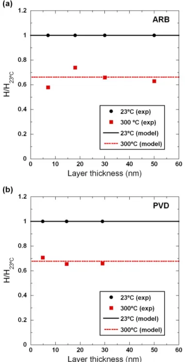
shown in Fig.4, the model predicts that the ARB interfaces would result in a lower hardness than the PVD interfaces, in agreement with the experimental observations. The predicted difference of 18% underestimates the actual experimental differences reported here (e.g., PVD NMMs are 30% harder than ARB NMMs forL=30 nm), but agrees with experimental results in other works.5The model, however, does not have an explicit dependence on layer thickness as shown in the supple-mentary material.23 Therefore, we find that the combined effect of elastic and plastic anisotropy and the predominant texture developed as a function of processing method can account for most of the differences between the hardness of the PVD and ARB processed NMMs with the same layer thickness.
The model also helps in understanding the actual drop of hardness with temperature at different layer thicknesses. Figures4(a)and4(b)compare the predicted and measured reduction in hardness (normalized by the room temperature hardness) with temperature for eachLand processing method. This normalization was selected in order to isolate the effect of temperature only. As shown, the magnitude of the reduction in hardness as temperature increases from 296 K to 573 K is well captured by the model. In agreement, forL>Lcrit, the regime where deformation is proposed to be controlled
052103-6 Moncl ´uset al. APL Mater.1, 052103 (2013)
FIG. 4. Predicted and measured reduction in hardness (normalized by the room temperature hardness) with temperature for eachLfor (a) PVD Cu/Nb NMMs and (b) ARB Cu/Nb NMMs.
attributed to higher dislocation mobility at elevated temperatures due to the lower stresses required for thermal activation, which is the thermally activated mechanism assumed in the simulations.
The predictions deviate from the measurements for the ARB NMM with L = 7 nm. The calculations assume no change in the thermally activated mechanism withL, and thus, the discrepancy atL=7 nm is consistent with the notion that a change in mechanism occurs at this length scale for the ARB, but not the PVD NMM. Specifically, the ARB and PVD NMM exhibit similar reductions in hardness with temperature above the critical layer thickness Lcrit, which can be attributed to
mechanism becomes predominant, likely dislocation-interface crossing, which prevails when the stress to bow out dislocation segments within the nano-layers exceeds the threshold stress for dislocation transmission across the interface.28,29 Our results on the ARB NMM suggest that the
interface crossing mechanism is accompanied by a substantial drop in hardness with temperature. The higherLcrit for ARB than PVD can be explained as an interface effect and is in agreement with indirect evidence provided by recent MD calculations suggesting that dislocation transmission across the ARB interface is easier than across the PVD interface.5,19,20
In summary, we report on the effect of nanolayer thickness and interface structure on the high-temperature mechanical behavior of two-dimensional nanocomposite metallic multilayers. Our study reveals the existence of a critical layer thicknessLcritat which the material is more resistant
to softening by elevated temperatures. We show for the first time thatLcrit depends on interface
structure, which provides indirect evidence thatLcritcorresponds to the layer thickness where the
chief deformation mechanism transitions from intralayer slip to interface crossing. These results imply that nano-layer size and interface structure can be tuned to achieve optimal high-temperature strengths in layered nanocomposite structures.
We acknowledge financial support from the European Union through the RADINTERFACES project (Grant No. 263273) and from the Spanish Ministry of Economy and Competitiveness through Grant No. MAT2012-31889 and the use of the microscopy infrastructure available at Laboratorio de Microscop´ıas Avanzadas (LMA), Instituto de Nanociencia de Arag´on (INA), University of Zaragoza (Spain). I.J.B., S.J.Z., and N.A.M. gratefully acknowledge support by the Center for Materials at Irradiation and Mechanical Extremes, an Energy Frontier Research Center funded by the U.S. Department of Energy, Office of Science, Office of Basic Energy Sciences under Award No. 2008LANL1026.
1H. Gleiter,Acta Mater.56, 5875 (2008).
2T. Chookajorn, H. A. Murdoch, and C. A. Schuh,Science337, 951 (2012).
3J. S. Carpenter, S. C. Vogel, J. LeDonne, D. L. Hammon, I. J. Beyerlein, and N. A. Mara,Acta Mater.60, 1576 (2012). 4A. Misra, J. P. Hirth, and R. G. Hoagland,Acta Mater.53, 4817 (2005).
5I. J. Beyerlein, N. A. Mara, J. S. Carpenter, T. R. Nizolek, K. Kang, S. Zheng, J. Wang, T. M. Pollock,J. Mater. Res.28, 1799 (2013).
6J. S. Carpenter, S. J. Zheng, R. F. Zhang, S. C. Vogel, I. J. Beyerlein, and N. A. Mara,Philos. Mag.93, 718 (2013). 7S. J. Zheng, I. J. Beyerlein, J. S. Carpenter, K. Kang, J. Wang, W. Z. Han, and N. A. Mara,Nature Commun.4, 1696
(2013).
8T. Hochbauer, A. Misra, K. Hattar, and R. G. Hoagland,J. Appl. Phys.98, 123516 (2005).
9K. Hattar, M. J. Demkowicz, A. Misra, I. M. Robertson, and R. G. Hoagland,Scr. Mater.58, 541 (2008). 10A. Misra, R. G. Hoagland, H. Kung,Philos. Mag.84, 1021 (2004).
11N. A. Mara, A. V. Sergueeva, T. Tamayo, X. Zhang, A. Misra, and A. K. Mukherjee,Mater. Sci. Eng., A493, 274 (2008);
Thin Solid Films515, 3241 (2007).
12J. F. Smith and S. Zheng,Surf. Eng.16, 143 (2000). 13A. Sawant and S. Tin,Scr. Mater.58, 275 (2008).
14J. C. Trenkle, C. E. Packard, and C. A. Schuh,Rev. Sci. Instrum.81, 073901 (2010). 15N. M. Everitt, M. I. Davies, and J. F. Smith,Philos. Mag.91, 1221 (2011). 16J. M. Wheeler, R. Raghavan, and J. Michler,Mater. Sci. Eng., A528, 8750 (2011).
17S. Lotfian, J. M. Molina-Aldareguia, K. E. Yazzie, J. Llorca, and N. Chawla,Philos. Mag. Lett.92, 362 (2012);J. Electron.
Mater.42, 1085 (2013).
18S. Lotfian, M. Rodr´ıguez, K. E. Yazzie, N. Chawla, J. Llorca, J. M. Molina-Aldaregu´ıa,Acta Mater.61, 4439 (2013). 19R. F. Zhang, T. C. Germann, X. Y. Liu, J. Wang, and I. J. Beyerlein,Scr. Mater.68, 114 (2013).
20I. J. Beyerlein, J. Wang, and R. F. Zhang,Acta Mater.61, 7488 (2013).
21I. J. Beyerlein, J. Wang, K. Kang, S. J. Zheng, and N. A. Mara,Mater. Res. Lett.1, 89 (2013). 22I. J. Beyerlein, J. Wang, and R. F. Zhang,APL Mat.1, 032112 (2013).
23See supplementary material athttp://dx.doi.org/10.1063/1.4828757for details on materials fabrication; details on high temperature nano-indentation; data supporting Figs.1and2; and crystal plasticity model description.
24J. S. Carpenter, R. J. McCabe, I. J. Beyerlein, T. A. Wynn, and N. A. Mara,J. Appl. Phys.113, 094304 (2013). 25S.-B. Lee, J. E. LeDonne, S. C. V. Lim, I. J. Beyerlein, and A. D. Rollett,Acta Mater.60, 1747 (2012). 26J. Schiotz and K. W. Jacobsen,Science301, 1357 (2003).
27L. Lu, X. Chen, X. Huang, and K. Lu,Science323, 607–610 (2009). 28S. L. Lehoczky,Phys. Rev. Lett.41, 1814 (1978).
![FIG. 3. TEM cross-sectional images of the indents in the PVD Cu–Nb NMM with L = 30 nm tested at: [(a) and (b)] RT and [(c) and (d)] T = 300 ◦ C](https://thumb-us.123doks.com/thumbv2/123dok_es/6760671.829746/5.918.160.755.134.509/fig-tem-cross-sectional-images-indents-nmm-tested.webp)