Microstructural characterization, optical and photocatalytic properties of bilayered CuO and ZnO based thin films
19
0
0
Texto completo
(2) https://cimav.repositorioinstitucional.mx/jspui/ was reached by bilayered films with roughly 50 at.% of Cu in the upper Zn–Cu oxide layer deposited onto a ZnO buffer film. Keywords: Thin films, Vapor deposition, Microstructure, Optical properties, SEM, TEM. Introduction Zinc Oxide is a wide band gap semiconductor, has received much attention because its ability to degrade a wide range of pollutants with high photocatalytic efficiency [1,3–6]; and it has been considered as a promising candidate for many applications, such as short wavelength light emitting diodes, laser diodes, piezoelectric transducers, varistors, phosphors, and transparent conducting films. In addition, ZnO exhibits high chemical and mechanical stability, non-toxicity along with its abundance in nature, which makes it a lower cost material [2–9]. However, the photocatalytic activation of ZnO used to eliminate or reduce noxious species takes place only under UV illumination [1,5,7,9]. ZnO absorbs only about 5% of sunlight, limiting its applicability with solar or ordinary lighting systems; thus significant progresses have to be made to render ZnO-based materials as a visible light photocatalyst. In order to absorb visible light, the band gap (BG) of ZnO has to be narrowed which can be achieved by doping with transition metal ions, e.g., Cu, Ni, Co, Cd, Ag, Mn [1,4,8–10]. Other alternative is the use of a multilayered structure with several sub-gaps covering different regions of the solar spectrum. At the same time, recent studies using heterostructures, where semiconductors with different band structures are superimposed, increasing the charge carriers’ life time and thus improving the photo activity [5,10–13]. As in the case of copper oxide which has been used to couple ZnO and TiO2 to form semiconductor. 2.
(3) https://cimav.repositorioinstitucional.mx/jspui/ composites that resulted in more efficient photocatalytic materials [10–13]. Also, Cu oxide is one of the most important compound semiconductors with many applications, such as magnetic storage media, field transistors, photovoltaic applications, superconductors, methanol synthesis and gas sensors. In this work, it is presented the synthesis, microstructural characterization and photocatalytic activity of bilayered CuO–ZnO/ZnO thin films onto borosilicate glass and fused silica substrates. The films were obtained by aerosol assisted chemical vapor deposition (AACVD), using a single precursor solution with optimized conditions to get high quality films. Different Cu/Zn molar ratios in solution were tried for the upper layer. The microstructure of the films was characterized by grazing incidence X-ray diffraction (GIXRD), scanning electron microscopy (SEM), high resolution transmission electron microscopy (HRTEM) and X-ray photoelectron spectroscopy (XPS). Microstructural characteristics of the films were discussed in correlation to the deposition parameters. Photocatalytic activity of the samples, for the degradation of a methylene blue (MB) solution, was determined after irradiation with an UV-A source.. 3.
(4) https://cimav.repositorioinstitucional.mx/jspui/ Experimental Synthesis: Thin films consisted of two layers; one buffer layer of pure ZnO, and the other a composite of Zn and Cu oxide. Different Cu and Zn content was tried, by changing the molar ratio of Cu and Zn precursors in solution. The bilayered films were synthesized on borosilicate glass substrates (5 cm x 5 cm), using AACVD technique in an experimental setup similar to that previously reported in [2]. The total concentration of all starting solutions was of 0.1 mol dm-3 in methanol (99.9% pure). Zinc Acetate 99.99% and Copper (II) nitrate hemipentahydrate 99.99% were used as precursor salts. An ultrasonic nebulizer (Sonaer PG-241) working at 2.4 MHz generated the aerosol that was conveyed by the carrier gas (air) and directed towards the substrate by a nozzle, which had a periodic movement at constant velocity (~1 cm min-1) to scan the whole surface of the substrate. Deposition temperature was fixed at 673 ± 1 K and air flux was set at 5 L min-1. Reference samples (control 1 and 2) consisted of only a ZnO layer. Other samples A to I, were synthetized with a first buffer layer of ZnO directly onto the borosilicate substrate and the second Zn–Cu oxide layer with different Cu/Zn at. ratio (see Table 1). Table 1 summarizes the principal deposition parameters used in this work. Characterization: Grazing incidence X-ray diffraction pattern was acquired to determine the crystalline phases present on the films using a Panalytical X-Pert system, working with a Cu Kα radiation (λ = 0.1542 nm) at 40 keV and 30 mA. Grazing incidence angle was set at 0.5°, and scanning angle 2θ was varied between 25° and 75°, with 0.02° and 12 s of step size and time, respectively. Surface morphology of the films were studied by SEM in a JEOL JSM-7401F and atomic force microscopy with a. 4.
(5) https://cimav.repositorioinstitucional.mx/jspui/ Veeco SPM MultiMode 4a working in contact mode. Energy Dispersive Spectroscopy (EDS) was performed with an Oxford Inca system attached to the electron microscope. Film thickness was measured from the transversal cross section of the samples analyzed by SEM. Cross sectional microstructure of the films was studied by HRTEM and nanobeam diffraction (NBD) in a JEOL JEM-2200FS microscope. Preparation of samples D, E and F for HRTEM analysis was carried out by focused ion beam (FIB) in a JEOL JEM-9320. Specular reflectance and transmittance spectra of selected films were measured in the UV–VIS–NIR interval in a CARY 5000 spectrophotometer. Chemical composition of the films was analyzed by XPS in an Escalab 250Xi spectrometer equipped with a monochromator.. 5.
(6) https://cimav.repositorioinstitucional.mx/jspui/. Photocatalytic activity measurement: The photocatalytic activity of the single ZnO and bilayered Zn–Cu oxide films was tested by the degradation of methylene blue in aqueous solution. The initial concentration of MB solution was fixed at 10-5 mol dm-3. In order to limit the contact area of the MB solution with the films, a Teflon ring of 2.5 cm of internal diameter and 1.1 cm3 of capacity was firmly placed on the surface of the samples. The film arrangements were introduced inside of an irradiation chamber and exposed to a UV-A lamp (UV BL-15) at 365 nm with time intervals of 120 and 240 min. Absorbance spectra of irradiated MB solution in contact with film were measured in a Perkin Elmer Lambda 35 spectrophotometer; where changes of MB absorbance peak at 664 nm was monitored as indicator of photocatalytic efficiency. Results Surface and cross sectional morphology: All the samples synthesized in this work showed high-quality as they were structurally uniform, non-light scattering, homogeneous and well adhered to the substrate. Representative secondary electron SEM micrographs of the surface morphology of single layered ZnO and bilayered Zn– Cu oxide films are shown in Fig. 1(a–e); the insets show the cross section of the corresponding film. All micrographs show that the films grew homogeneously, densely and crack free. Fig. 1a (single layer control 2) shows the uniformity of the sample of. 6.
(7) https://cimav.repositorioinstitucional.mx/jspui/ pure ZnO as a compact layer; exhibiting a grain morphology in the form of closely packed globular grains that appear evenly distributed over the surface. When adding 10 at.% of Cu in the second layer as in sample A (Fig. 1b) a drastic change in grain size and shape was noticeable, as grains appeared to have smaller non uniform shape. When Cu content in the second layer was increased to 40 (sample D) and 60 (sample F) at.%, as shown in Fig. 1c and d, the formation of small (10–50 nm) agglomerated structures was also visible. In these samples similar morphology and texture were observed, no significant variation among them were evidenced. In contrast, when having Cu at 80 (sample H) at.% in the second layer, as seen in Fig. 1e, a considerable change in grains size and shape was noticed, as a crack free, dense layer composed of evident granular formations (50–200 nm) was developed. Thickness of samples achieved by SEM cross section analysis is shown in the inset of Fig. 1. In general, thickness values ranged between 45 and 70 nm and any contrast image of the twolayered structure was perceptible by this backscattered electron technique. It is a consequence of the small difference of atomic number between Zn and Cu, as they are consecutive elements in the periodic table. Samples showed small variation in thickness as deduced from cross section measurements. Variations were of less than 13% in all samples. Three-dimensional atomic force micrographs in Fig. 2(a–c), scaned over an area of 3 x 3 lm, show the surface roughnes of samples control 2, D and F, respectively. Fig. 2a exhibits the globular grain microstructure previously seen on SEM micrograph for pure ZnO film. All samples in Fig. 2 consist of granular structures, with different grain size and rugosity; as seen also in SEM micrographs.. 7.
(8) https://cimav.repositorioinstitucional.mx/jspui/ RMS roughness values of these samples were calculated from AFM images. RMS roughness for control 2, sample D and F were 7 ± 1 nm, 2.0 ± 0.5 nm and 4.7 ± 0.3 nm, respectively. This means that when compared to pure ZnO, Zn–Cu oxide samples presented a reduction in roughness and grains size, result that is consistent with the morphology previously observed in SEM analysis. Crystalline structure: Grazing incidence X-ray diffraction patterns of the as deposited samples are presented in Fig. 3a and b. Films with different copper concentration in precursor solution are shown if Fig. 3a. All the films were polycrystalline and patterns were compared with a single layer of pure ZnO used as a reference (control 2). This film shows consistency with ZnO in the Zincite phase, according with the JCPDS PDF card 01-073-8765. When comparing diffraction patterns of pure ZnO with those of low copper concentrations (Fig. 3a), less than 40 at.%, it is seen that no considerable phase modification was reached, i.e. the location of the peaks did not change significantly as the peaks were only slightly shifted to high angles, indicating a decrease of interplanar distances, probably due to a stress generated during the synthesis, as a consequence of a difference in the thermal expansion coefficients of film and substrate. It is also observed a decrease in the intensities of the peaks with the increase of Cu contents, possibly due to an increased disorder in the ZnO film. In addition, for these low Cu concentration samples neither any Cu oxide nor other Cu phases were found, however surface morphology was affected (according to SEM micrographs). On the other hand, samples D to H show an evident difference when compared with the pure ZnO GIXRD pattern, indicating the presence of Cu oxide phases.. 8.
(9) https://cimav.repositorioinstitucional.mx/jspui/. A more detailed analysis of GIXRD for samples D and F at longer scanning times appear in Fig. 3b. It can be appreciated that the additional peaks correspond principally to CuO in the form of Tenorite that matched the data of JCPDS PDF card 03-065-2309. It is also observed a small shift of the diffraction angle to higher values, indicating a probable reduction on cell parameters. It is worthwhile to remark that (111) peak of Cuprite phase was probably overlapped with (101) peak of Zincite. Zn2+ (74 pm) and Cu2+ (73 pm) have almost the same ionic radius, which means that Zn and Cu can easily substitute between them into their crystal lattice. However, it was reported that a secondary phase of ZnO evolved when Zn concentration was greater than 8 at.% [14].. 9.
(10) https://cimav.repositorioinstitucional.mx/jspui/ Then this value would be approximately the solubility limit of Zn on CuO, consistent with other references [15]. In our case, Zn content was higher than the solubility limit.. In addition, high resolution transmission electron micrographs of samples D, E and F were obtained in order to locate and identify the Cu oxide phase within the upper layer of the films (Fig. 4). For both bright field scanning transmission electron microscopy (STEM) micrographs in Fig. 4a and b, of samples D and F, respectively; the formation of a bi-layered structure was slightly noticed. 10.
(11) https://cimav.repositorioinstitucional.mx/jspui/. As expected, contrast between layers was weak due to small difference in atomic number between Cu and Zn. However in Fig. 4b some darker region was visible, where Cu oxide phases were present; this contrast can be explained due to the high density of Cu oxide phases (>6 g cm-3) compared with ZnO (~5.6 g cm-3) [16]. Interplanar distances in Fig. 4b were determined, the bottom layer measured 0.264 nm that correspond to (002) plane of ZnO; and the upper layer had 0.236 nm which, agree approximately to (111) plane of CuO. Fig. 4c shows HRTEM micrograph of sample E. In this case due to diffraction contrast, it cannot distinguish ZnO and Zn–Cu oxide layers. Nevertheless, many crystallites showing lattice fringes were analyzed to identify the phases present in this sample. From this analysis, measured lattice fringes presented errors of less than 2%. Thus, family planes (101) and (002) of ZnO can be found in the buffer layer deposited onto the borosilicate glass (BSG) substrate (see Fig. 4c). More over in the Zn–Cu oxide layer it can be identified lattice fringes of planes (200) and ((111) of Tenorite (CuO) and plane (111) of Cuprite (Cu2O) phase; also some lattice. 11.
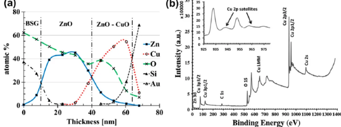
(12) https://cimav.repositorioinstitucional.mx/jspui/ fringes coincide with family planes of ZnO, also present in the layer. In this figure, planes of each phase was identified by Z for Zincite; T for Tenorite and C for Cuprite. To complement phase identification nanobeam electron diffraction was realized on each layer of sample E. Electron nanobeam size of around 30 nm was employed for this analysis; despite the small beam size used, a polycrystalline pattern was observed.. Fig. 4d and e show the NBD patterns of ZnO layer and Zn–Cu oxide layer, respectively. Table 2 presents interplanar distance deduced from several diffracted spots in each NBD pattern. It is shown that many family planes can be identified from Zincite phase, denoted by Z, in the buffer layer; and Tenorite (T), Zincite (Z) and Cuprite (C) phases in the upper Zn–Cu oxide layer. These results are consistent with lattice fringes measurements in HRTEM images. Composition of ZnO and Zn-Cu oxide layers by EDS and XPS: Average composition of the films was determined by EDS to check possible contamination, and to get the proportion of Cu and Zn in the second layer. For the ZnO buffer layer minor contamination with C was detected; moreover atomic ratio Zn/O was close to 1. In the upper Zn–Cu oxide layer, detailed analysis of samples D, E and F showed that Cu/Zn. 12.
(13) https://cimav.repositorioinstitucional.mx/jspui/ atomic ratio in film was very high, far from the initial molar ratio in solution. Fig. 5a shows a representative EDS line scan of sample E, similar to those obtained for samples D and F. It is shown the distribution of Si, O, Zn, Cu and Au in the cross section of the film. Si came from BSG substrate; and Au from the protection layer, deposited before FIB sample preparation. Cu concentration increases towards the surface of the film; consequently Zn diminished. In addition, Cu/O atomic ratio was higher than one, consistent with the identification of Cuprite in the HRTEM and NBD analysis. In addition, some samples were analyzed by XPS. The XPS spectra were measured in order to study the composition of bilayered samples D and F. The XPS spectra confirmed the high purity of films consisting only of Zn, O, Cu and just a small amount of C because of surface contamination, as shown in Fig. 5b. Details of the Cu2p spectra for sample F are shown in the inset of Fig. 5b; the Cu2p3/2 and Cu2p1/2 peaks were detected, it was determined the presence of Cu2+ as a predominant Cu specie, as the distinctive shake-up satellites for this chemical state, located at around 943 eV and 962 eV were visible, result that indicates the formation of a second layer of CuO consistent with XRD analysis. Results from sample D (not shown) were similar to those for sample F but shake-up satellites were less apparent, indicating a lower CuO content in the upper layer. Optical properties: Optical properties of several samples were studied by specular reflectance and transmittance spectra in the UV–VIS–NIR interval. Fig. 6a shows the specular absolute reflectance of samples D and F, in comparison with control 2 and borosilicate substrate. Results showed that Zn–Cu oxide films had a higher. 13.
(14) https://cimav.repositorioinstitucional.mx/jspui/ reflectance, principally in the visible region, than that of pure ZnO and bare substrate; consequence of the higher refractive index of Cu oxides in comparison to ZnO and glass. Fig. 6b shows the correspondent comparison of transmittance spectra of the same samples. It is shown that ZnO film has elevated transmittance, indicating high quality, and low dispersion of light. From these measurements, absorbance (A) spectrum was calculated for the films. Fig. 6c shows calculated absorbance in the 300– 1000 nm interval. Interestingly, it can be identified the absorption edge of BSG around 310 nm and that of ZnO at 365 nm. These spectra clearly show the increased absorption of bilayered samples in the visible region, i.e. a shift of the absorption band to lower energies, in the visible region.. 14.
(15) https://cimav.repositorioinstitucional.mx/jspui/. Moreover, the absorption in the visible region increases as the Cu content augmented; upper layer of sample F has around 60 at.% of Cu, in comparison sample D has only around 40 at.%. This indicates that the BG of Zn–Cu oxide material decreases with increasing Cu concentration, according to the approximate empirical rule of Vegard [17]. Since the bulk BG of ZnO (3.37 eV) is higher than that of Cu oxides, so the BG of Zn–Cu oxide should be lower than the BG of ZnO. The effective absorption coefficient α(λ) of the films was calculated from the spectral absorbance A (λ) and the total thickness t of the samples according to [18]:. Optical BG was determined following the Tauc’s plot method [19], using the relationship:. 15.
(16) https://cimav.repositorioinstitucional.mx/jspui/. where B is independent of the photon energy E, Eg is the optical band gap. It was considered an allowed direct transition for both the ZnO and Cu oxide. In our case, due to the clear separation of the absorption edges, it is expected a good approximation in the determination of the optical BG for both oxides. Fig. 6d and e shows the plot of (α.E)2 vs. E according to Tauc’s method. Two separate energy intervals were contemplated, correspondent to high energies (>3 eV) for ZnO, and low energies (<3 eV) for Cu oxide; the satisfactory linear fit obtained indicates an allowed direct BG. Extrapolation of this linear portion of the plot cut the energy axes at the optical BG energy. Table 3 presents the results of this analysis for ZnO in samples control 2, D and F; and for Cu oxide in samples D and F. In both oxides, the BG diminished as the Cu content of the upper layer increased. In the case of ZnO, the Eg decreased from 3.28, 3.22 to 3.17 eV for control 2, D and F samples. This behavior can be related to the fact 16.
(17) https://cimav.repositorioinstitucional.mx/jspui/ that ZnO was present in both layers (buffer and upper) thus, since the optical transmittance and reflectance spectra were obtained including both layers; then the possible diffusion of Cu into the small ZnO phase can modify the BG, according to the Vegard’s law. Similarly, for Cu oxide the optical BG for sample D was 2.11 eV and that of sample F was 1.99 eV. Photocatalytic activity: The photocatalytic activity of the samples (control 1, A to I) was tested by MB degradation under UV-A irradiation. Since the pathway for the selected dye exhibited a mayor absorption at 664 nm, this wavelength was taken as a reference to compare the degradation of the different samples (0% indicates no MB degradation). The photocatalytic activity was calculated and plotted for the different samples in Fig. 7, for two irradiation time (120 and 240 min). Both tests were repeated to confirm results. No significant degradation of MB was observed neither in the films with low and high Cu concentrations (samples A, B, C, G, H and I). However, those samples with Cu concentrations around 50 at.% (D, E and F), a considerable MB degradation (80–95%) was reached, very similar to that obtained for pure ZnO (control 1) sample. It was also clear from Fig. 7 that no significant general increase in the MB degradation was observed after longer irradiation time (240 min.). High activity for control 1 sample can be explained due to the higher absorbance of ZnO at the wavelength of irradiation (~370 nm). Samples D, E and F with Cu content around 50 at.%, showed a marked difference when comparing its photocatalytic efficiency with other Zn–Cu oxide films. However its activity was lower than control 1 sample, but it has to be considered that irradiation was with UV-A light. Following, optical absorbance shift. 17.
(18) https://cimav.repositorioinstitucional.mx/jspui/ to visible range for bilayered Zn–Cu oxide samples it should be expected a higher activity if visible light irradiation will be used. These experiments are in due course. Conclusions High quality bilayered ZnO/Zn–Cu oxide films were synthesized by AACVD technique. GIXRD results indicate the presence of ZnO Wurzite and Cu oxide phases. Results of SEM and HRTEM analysis of the cross sectional microstructure showed that the films were composed of compact and dense layers with no visible evidence of an interfacial boundary or porosity. It was also observed an evident change on the surface grain size distribution and morphology as Cu content increased. Optical absorbance determination of the bilayered films showed a clear shift of the absorption toward the visible range. Optical band gap of ZnO, was determined at 3.28, 3.22 and 3.17 eV, for control 2, D and F samples, respectively. For Cu oxide, the optical band gap in samples D and F, was 2.11 and 1.99 eV, respectively. Photocatalytic activity of the samples, for the degradation of a 10-5 mol dm-3 solution of methylene blue (MB), was determined after 120 and 240 min of irradiation with an UV-A source. Best bilayered films with roughly 50 at.% of Cu in the upper Zn–Cu oxide layer had around 90% of MB degradation in 240 min. Acknowledgments The Author thanks to W. Antúnez-Flores, K. Campos-Venegas, C. Leyva-Porras and E. Torres-Moye, S. Miranda, M. Lugo, O. Esquivel, R. Ramírez for their technical support. This work was partially supported by CONACYT project No. 106655. References [1] R. Ullah, J. Dutta, J. Hazard. Mater. 156 (2008) 194–200.. 18.
(19) https://cimav.repositorioinstitucional.mx/jspui/ [2] P. Amézaga-Madrid et al., J. Alloys Comp. 509S (2011) S490–S495. [3] M. Rezapour, N. Talebian, Mater. Chem. Phys. 129 (2011) 249–255. [4] N. Talebian, M.R. Nilforoushan, Z. Salehi, Ceram. Int. 38 (2012) 4623–4630. [5] R.T. Sapkal et al., J. Photochem. Photobiol. B 110 (2012) 15–21. [6] P. Jongnavakit et al., Appl. Surf. Sci. 258 (2012) 8192–8198. [7] L. Ma et al., Appl. Surf. Sci. 257 (2011) 10036–10041. [8] M.B. Rahmani et al., Sen. Lett. 7 (2009) 1–8. [9] S. Anandan, N. Ohashi, M. Miyauchi, Appl. Catal. B 100 (2010) 502–509. [10] S.S. Lee et al., Water Res. 47 (2013) 4059–4073. [11] P. Sathishkumar et al., Chem. Eng. J. 171 (2011) 136–140. [12] R. Saravanan et al., Mater. Sci. Eng. C 33 (2013) 91–98. [13] B. Li, Y. Wang, Superlattices Microstruct. 47 (2010) 615–623. [14] _Ibrahim Y. Erdog˘an, J. Alloys Comp. 502 (2010) 445–450. [15] D. Prabhakaran, A.T. Boothroyd, J. Cryst. Growth 250 (2003) 77–82. [16] John W. Anthony, Richard A. Bideaux, Kenneth W. Bladh, Monte C. Nichols (Eds.), Handbook of Mineralogy, Mineralogical Society of America, USA, 2013 (http://www.handbookofmineralogy.org/august). [17] A.R. Denton, N.W. Ashcroft, Phys. Rev. A 43 (1991) 3161–3164. [18] N.F. Mott, R.W. Gurney, Electronic Processes in Ionic Crystals, second ed., Dover, New York, 1964. [19] P.S. Kireev, Semiconductor Physics, MIR, Moscow, 1966 (Chapter 8).. 19.
(20)
Figure
Documento similar
