Hybrid clock and data recovery for a high speed transceiver implemented on a FPGA
Texto completo
Figure


Documento similar
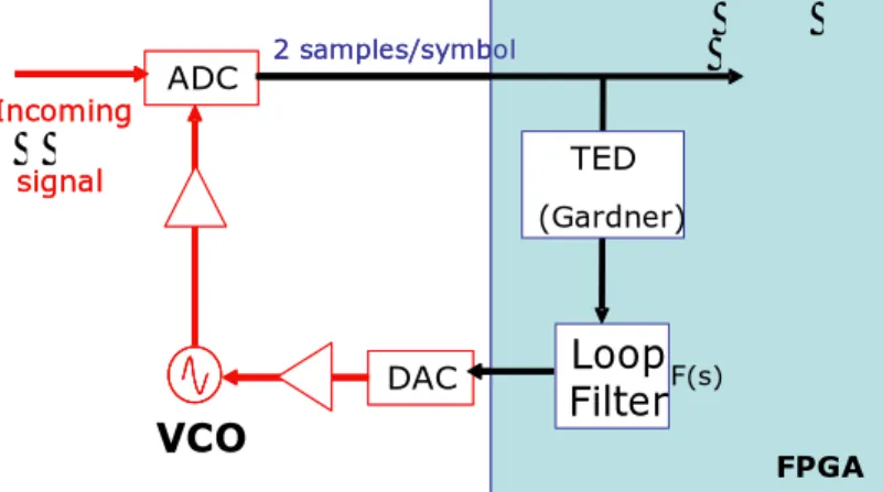
The proposed architecture has been implemented in a Xilinx Zynq Ultrascale+ MPSoC platform (XCZU9EG-2FFVB1156E FPGA with a grade speed of -2) at a work frequency of
The expansionary monetary policy measures have had a negative impact on net interest margins both via the reduction in interest rates and –less powerfully- the flattening of the
Ø SPICE is an information system that uses auxiliary data to provide Solar System geometry information to scientists and engineers for planetary missions in order to plan and analyze
Therefore, the rebuilding technique is more appropriate for custom hardware (FPGA or ASIC) implementation than for digital signal processor (DSP) or microcontroller, as in
In this paper a current sensorless control method of power factor correction for a boost converter based on pre-calculated duty cycle values is proposed, which is similar to
(hundreds of kHz). Resolution problems are directly related to the resulting accuracy of the computation, as it was seen in [18], so 32-bit floating point may not be appropriate
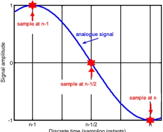
Using the appropriate control signals, the relative phase of the input clock, CLKIN, and the output clock, CLK0, can be changed in steps of 1/256 of the clock period (see Fig.
In this paper, decimal carry-chain and ripple-carry adders have been implemented on Virtex-4 Xilinx FPGA platforms, for a number of operand sizes; comparative performances are
