A characterization on hybrid lead halide perovskite solar cells with Ti02 mesoporous scaffold
45
0
0
Texto completo
(2) Abstract The booming perovskite solar cells (PSCs) field has emerged from the solid-state dyesensitized photovoltaic cells with significant advances in solar to electric power conversion efficiency in a relatively short time. However, a lot a research is currently trying to explain many poorly understood aspects of its operating modes. Current density-voltage ( ) solar cells response has always been a fundamental photovoltaics characterization, and specifically on PSCs it presents an anomalous hysteretic behavior whose origin has been mainly addressed to ferroelectric or ionic effects. Here we show, on the basis of a CH3NH3PbI3-xClx with a mesoporous TiO2 scaffold based solar cells characterization, that such anomalous hysteresis can be better explained in terms of interface capacitive ionic slow dynamic processes. Furthermore, we present a methodological review for the proper performance of MottSchottky analysis in PSCs stressing on the importance of complementary impedance spectroscopy characterization. On this issue we highlight our finds of an analogous hysteresis and an exponential capacitance excess on capacitance-voltage characteristics that can be associated with an exponential density of localized states below the conduction band. Our calculus of the corresponding total density of localized states supports our stands for interface processes.. 2.
(3) Content Abstract ............................................................................................................................. 2 Acknowledgements .......................................................................................................... 4 List of symbols, acronyms and abbreviations .................................................................. 5 1. Introduction .................................................................................................................. 7 2. Experimental............................................................................................................... 10 2.1. CH3NH3PbI3-xClx based solar cells fabrication ................................................... 10 2.2. CH3NH3PbI3 pellets fabrication........................................................................... 11 2.3. Samples Characterization .................................................................................... 12 3. Current density-Voltage characterization ................................................................... 13 3.1. Current density-Voltage characterization under illumination ............................. 14 3.2. Dark current density-voltage characterization ..................................................... 21 4. Sawyer-Tower circuit measurements ......................................................................... 25 5. Capacitance-voltage characterization ......................................................................... 28 6. Conclusions ................................................................................................................ 34 References ...................................................................................................................... 35 Annex figures ................................................................................................................. 45. 3.
(4) Acknowledgements To Generalitat Valenciana for the grant GRISOLIAP2014/035 To the personal and technique from the Group of Photovoltaic and Optoelectronic devices of the Institute of Advanced Materials, and the Servei Central d’Instrumentació Científica at Universitat Jaume I de Castelló. To Antonio Guerrero for the CH3NH3PbI3 pellets fabrication And specially, To Elena Mas-Marza for her directions and express implication during the CH3NH3PbI3-xClx based solar cells fabrication And To Professor Germà Garcia-Belmonte for his wisdom. 4.
(5) List of symbols, acronyms and abbreviations. : difference between bias scan direction operator : vacuum permittivity constant : MAPI relative dielectric constant : relative dielectric constant : solar to electricity power conversion efficiency : wave length : incident spectral photon flux density at AM1.5 : electric flux : MAPI work function : TiO2 work function : MAPI electron affinity : TiO2 electron affinity. : holes chemical potential (quasiFermi level) : electrons chemical potential (quasi-Fermi level) : band gap :external quantum efficiency : top of the valence band energy : vacuum level energy : fill factor FS: forward bias scan direction FTO: fluorine doped tin oxide : generation coefficient : density of states as a function of electrons chemical potential (quasi-Fermi level). : light-absorbing area AC: alternating current : diode total area AM: air mass. : Planck constant HTM: holes transport material : current. BS: backward bias scan direction : saturation current density : transient current density at which there is zero voltage : current density : saturation current density : capacitive current density : photo-current density : short circuit current density : space charge recombination current density : steady-state current : current density-voltage (curve). : light speed : capacitance per unit area : reference capacitor in the STC : sample capacitance in the STC : capacitor plate separation distance DC: direct current DFT: density function theory DOS: density of states DSSC: dye-sensitized solar cell : energy : electric field : bottom of the conduction band energy : Fermi level energy. : Boltzmann constant : electrons diffusion length 5.
(6) : holes diffusion length : localized states layer width. : load resistance : recombination resistance : series resistance : shunt resistances. : diode ideality factor MA: methyl ammonium (CH3NH3+) MAPI: CH3NH3PbI3, or indistinctly CH3NH3PbI3-xClx. : bias scan rate SEM: scanning electron microscopy STC: Sawyer-Tower circuit. : density of electrons in the conduction band : conduction band density of states : total density of localized states : MAPI acceptor defect concentration : TiO2 donor defect concentration : valence band density of states. : potential drop across the reference capacitor in the STC : transient voltage at which there is zero current density : applied potential : total built-in potential : partial built-in potential at the MAPI side : partial built-in potential at the TiO2 side : bulk resistance potential drop : contact resistance potential drop : open circuit voltage : series resistance potential drop. : output power density : polarization : density of holes in the valence band PSC: perovskite solar cell : elementary charge : total charge. XRD: X ray diffraction : temperature : time : stabilization time. : space charge width : space charge width at TiO2 : space charge width at MAPI. : bulk resistance : contact resistance. 6.
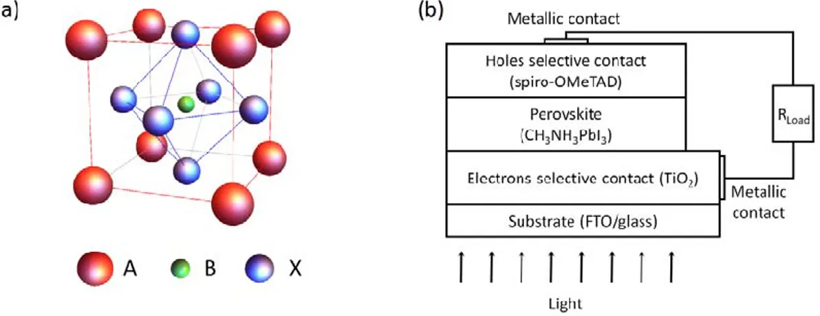
(7) 1. Introduction More than 85% of the current world primary energy supply comes from fossil and mineral fuels,1 which as non-renewal energetic sources will eventually reach its physical limit. The pace at which those resources are consumed is catalyzed by both population2 and energy use per capita increase,3 and even more immediate than the fossil fuels availability decline is the rising negative environmental effect of such global energetic scheme.4 In that scene a future sustainable society with similar or better than our current standard of livings depends on the proper transition to renewal energy technologies. The Sun power projected on Earth surface ( ) gives approximately 35 5 000 times the world energy consumption per year. Such tremendous potential and the significant non-detrimental impact of its exploitation6 make photovoltaic technologies one of the most feasible options for humankind future sustainable development. Among the different photovoltaic generations the pioneer technology has been the crystalline silicon, whose over more than 60 years7 continuous progress has become it in the industry leader.8 Aiming to reduce costs and enhance versatility, newer technologies have been developed such as typical CdTe and CIGS thin film solar cells 9 or the so called “emerging technologies”, for instance, dye-sensitized solar cells (DSSCs)10 and organic solar cells.11 However, maybe the most recent and promising photovoltaic devices are the denominated perovskite solar cells (PSCs), that in about three years12 have already achieved solar to electricity power conversion efficiency ( ) values as high as 20.1%.13 It can be said that these all solid state devices have arisen from the field of dye-sensitized solar cells14 with the innovating inclusion of hybrid lead halide perovskites as absorber material. The perovskites is the denomination of a wide family of materials with the general formula ABX3 and the crystal structure of the mineral perovskite, the calcium titanate. Figure 1.1a illustrate such structure where the A cation is coordinated with twelve X ions and the Β cation with six. Thus, the A cation is normally found to be somewhat larger than the Β cation.15 Several properties have been found for these materials for many years, e.g. ferroelectric,16 piezoelectric,17 ferromagnetic,18 antiferromagnetic,19 thermoelectric,20 insulating,21 semiconducting,22 conducting,23 and superconducting.24 However, it was not until 2006 when photovoltaic application was first reported for devices with CH3NH3Pb(I3, Br3) perovskites as absorber material, broadcasting less than 1% of for all solid-state cells.25 These first works and further optimizations26 resulted in the “perovskite phenomena” trigger when in 2012 up to 10% efficiency CH3NH3PbI327 and mixed halide CH3NH3PbI3-xClx28 based solid-state devices were obtained. The PSCs structure basically consists in a light harvesting perovskite sandwiched between the electrons and holes selective contacts. Several materials variation has been reported,29 however probably the most extensively studied arrangement is that showed 7.
(8) in figure 1.1b where on top of the FTO/glass substrate the TiO2 layer is growth, then the CH3NH3PbI3 perovskite and later the 2,2(7,7)-tetrakis-(N,Ndipmethoxyphenylamine)9,9(-spirobifluorene) (spiro-OMeTAD). The metallic contacts are often made of gold in order to better wire connections with the load ( ).. Figure 5.3: (a) Generic perovskite crystal unit cell structure. (b) Typical structure of PSCs.. The TiO2 is a bandgap semiconductor30,31 which has been widely employed in photovoltaic applications mainly in the field of DSSCs. It has an strong intrinsic n-type conductivity, is transparent to visible light, has high refractive index and low absorption, and can be growth by many low cost techniques, e.g. spin coating and spray pyrolysis.30 For PSCs structures is presented in two main configurations: (i) as a compact layer and (ii) as a mesoporous scaffold. These two variants, as a matter of fact, define two main device architectures: planar and mesoporous (meso). Among the different substitutes as electron-selective contact some examples can be mentioned: C60,31 graphene/TiO2 nanocomposites,32 and ZnO.33 The spiro-OMeTAD as hole transport material (HTM) also comes from the solid-state DSSCs field.34 Its utilization has been found to increment the cell series resistance, due to its low intrinsic hole-mobility and -conductivity.35,36 On the other hand, this effect is greatly compensated for by the beneficial reduction in recombination rate that it is liable of.36 Furthermore, spiro-OMeTAD plays a very important role by isolating the perovskite from the critically degrading effect of moisture from the humidity present in ambient air.35 Alternatively, different molecules and polymers,37 and also inorganic CuI38 have been also used as hole-selective contacts. The CH3NH3PbI3 , or CH3NH3PbI3-xClx, perovskite (indistinctly MAPI in the next, unless clarifying would be need) has been found to be a direct bandgap 39,40 41,42 semiconductor with high absorption coefficient, large carrier mobility43,44 and easy fabrication processes, e.g. dip and spin coating.42,45,46 In the high temperature cubic phase, the methyl ammonium organic cation CH3NH3+ (MA) is A in the perovskite general formula while the lead and the halogen are B and X, respectively (see also unit cell structure in figure 1.1a).47 Interestingly, it has been pointed that the electrical intrinsic conductivity of MAPI can be modified from p-type to n-type by 8.
(9) controlling growth conditions, i.e. by setting the concentration of elemental defects derived from Frenkel defects,48 such as Pb, halogen, and MA vacancies, that form shallow levels near band edges.49 The intensive research activity has been and still is pushing the frontiers further in terms of cost, efficiency, and stability aiming to achieve competitive industrial scalability in the near future. Nevertheless, several issues of PSCs are poorly comprehended. Among the different subjects where the attention has been most focused are: (i) the recent discovered giant switchable photovoltaic effect;50 (ii) the interpretation of the MAPI capacitance frequency dependence with an “apparent” giant dielectric constant observed at ultraslow frequency, and amplified under illumination;51 (iii) the slow electrical material response under light irradiation;52 and (iv) the anomalous hysteresis of the current-voltage curves.53 Particularly on the later topic, a controversial debate lies in the literature discussing mainly between ferroelectric and ionic effect based behaviors. In this study, as a contribution to the better understanding mainly of the last three right above mentioned issues (ii-iv), an electrical characterization on CH3NH3PbI3-xClx with a mesoporous TiO2 scaffold based solar cells is presented (experimental section in chapter 2). By means of the dark and under illumination current density-voltage ( ) characteristics we explore the carriers kinetics at different conditions; e.g. irradiance, voltage swept rate and sense, temperature (chapter 3). Using basic curve model equations, the role of the different characteristic parameters (e.g. photogenerated and saturation currents, series and shunt resistances, diode ideality factor) in the general performance of the cell and specifically on the anomalous curve hysteretic behavior is elucidated. In order to rule out the possible presence of ferroelectric behavior in the devices, Sawyer-Tower circuit measurements were carried and no typical hysteretic polarization-field loops were obtained (chapter 4). The charge profile and band energy representation at the main interface, i.e. between the TiO2 and the MAPI, were investigated via capacitance-voltage measurements (chapter 5). Furthermore, here we present a methodological review for the proper performance of Mott-Schottky analysis in PSCs stressing on the importance of complementary impedance spectroscopy characterization. Resultantly, further evidence that suggest a capacitive origin of the hysteresis phenomena and its relation with slow ionic processes at the MAPI interfaces is summarized in the conclusive chapter 6.. 9.
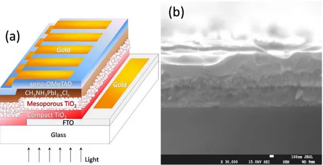
(10) 2. Experimental In this chapter we present the detailed description for the fabrication of the samples (sections 2.1 and 2.2) and the characterization technique (section 2.3). All the PSCs studied in this work where based on CH3NH3PbI3-xClx perovskite absorber material, whose fabrication is described in the following segment (section 2.1). The characterization of these devices by , Sawyer –Tower circuit and capacitance– voltage measurements are developed in chapters 3, 4 and 5, respectively. Specifically in chapter 4, the resulting polarization-field Sawyer-Tower circuit measurements on CH3NH3PbI3 pellets are also presented. The fabrication of these macroscopic pellets is described in the section 2.2 of this chapter.. 2.1. CH3NH3PbI3-xClx based solar cells fabrication The device structure used in this study has the CH3NH3PbI3-xClx perovskite in a TiO2 mesoporous scaffold sandwiched in a sequence of layers of the type: FTO/TiO2(compact)/TiO2(mesoporous)/MAPI/spiro-OMeTAD/Au (figure 2.1). All the studied cells were prepared over FTO glasses (25×25mm, Pilkington TEC15, ~15 Ω/sq resistance), which were partially etched with zinc powder and HCl (2 M) in order to avoid short circuits, obtaining 0.25 cm2 of active electrode area. The substrates were cleaned with soap (Hellmanex) and rinsed with milliQ water and ethanol. Then, the sheets were sonicated for 15 minutes in a solution of acetone: isopropanol (1:1 v/v), rinsed with ethanol and dried with compressed air. After that, the substrates were treated in a UV-O3 chamber for 20 min.. Figure 2.1: MAPbI3 based cell structure sketch (a) and cross section SEM image (b). 10.
(11) For the electrons selective contact, first the TiO2 blocking layer was deposited onto the substrates by spray pyrolysis at 480ºC, using a titanium diisopropoxidebis(acetylacetonate) (75% in isopropanol, Sigma-Aldrich) solution diluted in ethanol (1:39, v/v), with oxygen as carrier gas. The spray was performed in 4 steps of 12 s, spraying each time 10 mL (aprox.), and waiting 1 min between steps. After the spraying process, the films were kept at 480ºC for 5 minutes. Subsequently, a UV-O3 treatment was performed for 20 minutes. For the scaffold growing, the mesoporous TiO2 layer was deposited by spin coating at 4000 rpm during 60 s using a TiO2 paste (Dyesol 18NRT, 20 nm average particle size) diluted in terpineol (1:3, weight ratio). After drying at 90ºC during 10 min, the TiO2 mesoporous layer was heated at 470ºC for 30 min and later cooled to room temperature. The thickness determined by Scanning Electron Microscopy was of approximately 200 nm observed in Figure 2.1b The perovskite precursor solution was prepared by reacting 2.64 mmol of CH3NH3I and 0.88 mmol of PbCl2 (3:1 molar ratio) in 1 mL of DMF. Then, 100 µl of this solution was spin-coated inside a glovebox, at 2000 rpm for 60 s. After the deposition, the substrate was kept at 100ºC for 10 min. Next, the substrates were heated at 100ºC during 90 min in an oven under air stream. Subsequently, the perovskite films were covered with the hole-transporting material (HTM, 300 nm-thick) by spin coating at 4000 rpm for 30 s under air conditions, using 100 μL of spiro-OMeTAD solution. The spiro-OMeTAD solution was prepared by dissolving in 1 mL of chlorobenzene 72.3 mg of (2,2′,7,7′-tetrakis(N,N′-di-p-methoxyphenylamine)-9,9′-spirobifluorene), 28.8 μL of 4-tert-butylpyridine and 17.5 μL of a stock solution of 520 mg/mL of lithium bis(trifluoromethylsulphonyl)imide in acetonitrile. Finally, 60 nm of gold was thermally evaporated on top of the device to form the electrode contacts using a commercial Univex 250 chamber, from Oerlikon Leybold Vacuum. Before beginning the evaporation, the chamber was evacuated until pressure of 2×10⁻⁶ mbar. The active electrode area of 0.25 cm2 per pixel is defined by the FTO and the Au contacts.. 2.2. CH3NH3PbI3 pellets fabrication The synthesis of the CH3NH3PbI3 was carried by slow evaporation in gammabutyrolactone (GBL) containing stoichiometric amounts of methyl ammonium iodide (1 eq) and lead iodide (1 eq). The mixture was placed in an open crystallization dish into a well ventilated oven at 170 °C during 3 h. The black powder was characterized by XRD to confirm the pure perovskite crystallographic form (figure 2.2a). Alternatively, SEM analysis also shows a highly crystalline nature of the powder (figure 2.2b). The pellets were prepared by pressing at 6 ton 250 mg of MAPBI3 powder into a 1.3 cm diameter cylinder pellet die. The resulted thickness was of 500 μm as evaluated by profilometry (figure 2.2c).. 11.
(12) Figure 2.2: MAPI pellet XRD (a), SEM image (b) and profilometry signal (c).. 2.3. Samples Characterization Current density−voltage curves were recorded under AM 1.5 simulated sunlight (ABET Technologies Sun 2000) previously calibrated with an NREL-calibrated Si solar cell. The obtained solar to electricity power conversion efficiency using a 0.10 cm2 mask were about 9.5%. The dark curves were measured with a PGSTAT-30 from Autolab using different scan rates. For the measurement of capacitance spectra as a function of the temperature and the voltage, an Alpha-N analyzer was employed with a Quatro Cryosystem temperature controller from Novocontrol Technologies. The AC voltage perturbation was of 10 mV. The same cryosystem was employed for the dark current density−voltage curves varying temperature. For the performance of measurements in the Sawyer-Tower circuit set up, the potential signals were applied with an Agilent 33220A 2MHz function arbitrary waveform generator and the measurement of the resulting signals from the sample were carried out with a Hewlett Packard Infinium oscilloscope (500 MHz, 1GSa/s).. 12.
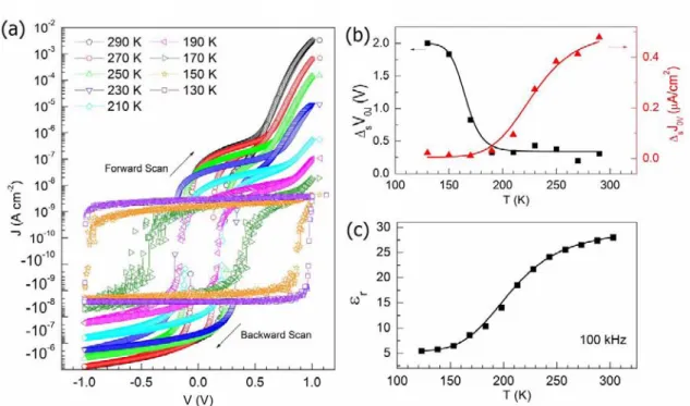
(13) 3. Current density-Voltage characterization The current density-voltage characterization constitutes a fundamental tool for understanding the solar cells operation; and its performance under standard illumination conditions (air mass (AM) 1.5, 100 mW cm−2 irradiance)54 is the established method for measuring the solar to electricity power conversion efficiency. Typically, a bias is applied across the device terminals sweeping the proper voltage range while current through an external circuit is been measured in a steady-state power output condition. However, it seems that such steady-state power output condition is not so easy to hold for MAPI based solar cells. The curves itself has been the focus of a lot of discussion due to its characteristic anomalous hysteretic behavior whose identification,55 description and understanding have been tackled in several studies. In this sense, H.J. Snaith et al.53 found that the scan direction and rate at which the bias is swept and the specific device architecture severely modify the curve shape, and proposed three possible explanations: (i) filling and emptying of trap states, (ii) ferroelectric effect, and/or (iii) migration of excess ions, as interstitial defects (iodide or methylammonium). H.S. Kim and N.G. Park56 pointed the increase of the crystal size of MAPI and the presence of mesoporous TiO2 film as alleviating factors for the hysteresis, and by correlating the amount of hysteresis with the size of perovskite and mesoporous TiO2 layer thickness, suggested that the origin of hysteresis is due to the capacitive characteristic of MAPI. An alternative interpretation was made by H.W. Chen57 who affirmed that the greater magnitude of hysteresis in the case of a planar heterojunction and Al2O3 scaffolds in comparison to mesoporous TiO2 structures indicates the significance of the bulk property of perovskites rich in ferroelectric domains as an origin of hysteresis. A theoretical support to this hypothesis was afforded by J.M. Frost et al.58 through ab initio molecular dynamics numerical simulations and J. Wei et al.59 interpreted the scan range and rate dependency as is well explained by the ferroelectric diode model. Back on the issue of the presence of the mesoporous TiO2 layer hysteretic impact on, N.J. Jeon et al.60 also observed that such effect is critically dependent of the mesoporous scaffold thickness, reaching a minimum at 200 nm and enhancing for lesser or larger thicknesses. In other direction, R.S. Sanchez et al.61 showed that the hysteresis is enhanced at high sweep rates, and hence it could be a capacitive current ( ) effect, which is a widely recognized feature in liquid electrolyte dye solar cells (DSCs). In addition, O. Almora et al.62 studied the same capacitive trend, but in dark conditions, correlating the hysteretic behavior with the capacitance excess observed at low frequencies that attributed to ionic electrode polarization. Another contribution was made by E.L. Unger et al.63 who concluded that measurement delay time, and light and voltage bias conditions prior to measurement can all have a significant impact upon the shape of the measured curve, and by utilizing alternative selective contacts found that the contact interfaces have a big effect on transients in MAPI-absorber devices. Furthermore, R. Gottesman et al.52 studied the photoconductivity slow response of MAPI samples and proposed that under solar cell working conditions the structure of the MAPI perovskite varies depending on the applied bias and/or the light intensity on the basis of density function theory (DFT) calculations that predicts an slow alignment between the field-dependent 13.
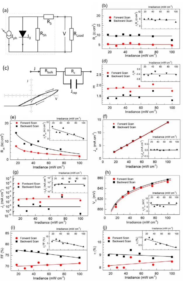
(14) ionic rotation and the inorganic MAPI scaffold. On the other hand, Y. Shao et al. 31 showed the defect states on the surface and grain boundaries of the perovskite materials to be an originating factor for the photocurrent hysteresis and that fullerene layers (PCBM/C60) deposited on perovskites can effectively passivate these charge. Moreover, W. Tress et al.64 argued, from his study on curve rate dependency and transient photocurrent, that the hysteretic behavior in timescales of seconds to minutes is most likely due to ions, which accumulate at the interfaces of the electrodes and screen the applied field independent of illumination. Also H. Zhang et al.65 stated that the accumulation of mobile ions in the hybrid perovskites causes space charge at interfaces and pointing that the presence of a thick PC61BM layer in a device achieve very low interface charge density ( ) and thus it leads to hysteresis-free characteristics. The hypothesis was also supported by J. Beilsten-Edmands et al.,66 who also rejected the ferroelectric effect idea, and further theoretical agreement was provided by S. van Reenen et al.67 who achieve hysteresis in his modeled characteristics by including both ion migration and electronic charge traps, serving as recombination centers in a numerical drift-diffusion model.. 3.1. Current density-Voltage characterization under illumination The above reviewed features and explanations illustrate the focal issues currently in debate. Herein we first investigate curves evolution with irradiance exploring, at the same scan rate ( ), the forward (FS) and backward (BS) bias scan directions, i.e. from short circuit to forward bias and vice versa, respectively. No prior voltage bias or illumination treatment was applied in order to avoid MAPI structure modification52 or possible light or voltage enhanced degradation68. As it can be seen in figure 3.1b, the hysteretic called difference between voltage scan directions affects directly the output power , which is in general greater in the BS (solid lines) than in the FS (dashed lines), mainly in the region of the cell´s operation point. At first appearance, the curves follow the typical solar cells shape, which is the classic 69 Shockley ideal-diode equation shifted in the current axis due to the photo-generated current. However, a more realistic than the later approximation must be taken into account in order to properly considerate some effects like the recombination in the depletion region, parasitic series resistances and leakage currents through the junction, which are of noteworthy significance for the device operation understanding. Thus, it is suitable to employ the widely used model that correlate the equivalent circuit of figure 3.2a where the load at a given voltage is connected to the cell, which is a photo-current source shunted by a diode and a resistor , all in series with another resistor . The solution of this circuit and further empirical approximations54,70-72 lead us to the following equation (. where. ). ,. (3.1). is the saturation current density (A cm-2, where the area is the diode total ); is the elementary charge; 14.
(15) is the Boltzmann constant; is the temperature (K); is the dimensionless diode ideality factor; is the photocurrent (A cm-2, where the area is the light-absorbing ); and and are the series and shunt resistances ( cm2, with ), respectively. Complementary concepts like the open circuit voltage ( ), the short circuit current ( ), the fill factor ( ), and the solar to electricity power conversion efficiency ( ) will be tackled in the forthcoming.. Figure 3.1: Density current-voltage (a) and corresponding output power-voltage (b) curves for different irradiances illumination expresend as percentage of 100 mW cm-2 at AM 1.5. Dashed and solid lines identify the curves where the voltage was swept in forward and backward directions, respectively.. The resulting calculated values from fitting of figure 3.1 curves to equation 3.1 at 300 K of temperature are displayed in figure 3.2b-h (see also annexed figure A1). The general trends in all cases were highlighted with solid lines in order to facilitate the data comprehension. In that sense, it was also considered to introduce the operator which applied over a magnitude gives the difference between such magnitude obtained from the curve measured in BS with respect to FS voltage swept direction; i.e. . Subsequently, the results of over the respective parameters in figure 3.2b,d-h were included as inset. The series resistance characterizes two major resistive parasitic contributions: (i) the bulk resistance ( , that includes the TiO2 and MAPI bulks, and the metal bulk of the wires and connectors) and (ii) the contact resistance ( , that responds for the interfaces between the metal contacts (Au) and the junction: i.e. through the FTO to the TiO2 and through the spiro-OMeTAD to the MAPI). About the later, precisely the contact resistance via the spiro-OMeTAD has been found as the dominating contribution by a recent work about the selective contact role in MAPI based cells.36 In our case, the general trend (figure 3.2b) results in approximately light-independent constant behaviors around and for FS and BS, respectively, which are 36,73-75 values commonly reported in literature. It is interesting that is , which is almost the at FS. It suggests a strong direct impact of the hysteresis originating process on the main series resistant contributing element. Then, let us assume that the total potential drop that is responsible of have the form (3.2) 15.
(16) where and are the series resistance potential drops at the bulk and at the interface MAPI-back contact, respectively. Therefore, it would be possible the formation of a mobile ions space charge at the contact where a displacement current ( ) were ruled by the electric flux variation with time ( ). Consequently, it could result in a series connection of two resistors:. (. and. (3.3). ),. (3.4). shunted by the capacitive current per. source. ,. (3.5). where is the MAPI relative dielectric constant, is the vacuum permittivity constant, and is the electric field (see circuit sketch in figure 3.2c). Following this idea, at slow enough voltage scan rates ( ) the curve hysteresis should 62 disappear, which have been previously noticed as a capacitive feature and we confirm in this chapter section 3.2. In fact, a simple simulation made in the Electronics Workbench software with the circuit of figure 3.2a but using the circuit of figure 3.2c as , is capable of reproduce in a gross way the curve hysteresis for faster enough sweeps (see inset of figure 3.2c). This capacitive effect that we have ascribed to the contact resistance modifies the entire curves, hence it is to expect that when fitting the rest of parameters from equation 3.1 should mathematically “feel” the change between bias scan sense and rate. Therefore, if we assume this hypothesis, then not conclusive interpretations should be made from the rest of calculated parameters, given that they are mainly related with principal junction (TiO2/MAPI) phenomena: the photodiode. However, there are possible implications for our proposal that we develop in the forthcoming precisely related with slow dynamic charge rearrange repercussion on MAPI space charge at the main junction with the TiO2. The ideality factor exhibits approximately no changes with scan direction (approximately constant ) or illumination intensity (figure 3.2d). The later is expected given that does not characterize the photo-generation process, but the prevalence of diffusion in the neutral region ( or recombination in the space charge region ( processes in the dark p-n junction of the cell (the diode), that has been identified between the MAPI and the TiO2.76-79 Our resultant values lie around and for BS and FS, respectively, similarly to earlier registered results 38,73,75,80 and pointing to depletion region recombination predominance in the kinetics of the device. This increase of recombination in one bias scan sense with respect to the other could be mainly at the interface, where the injected carriers interact with the widely studied TiO2 density of states (DOS),81 which is rich in bandgap traps localized states. Furthermore, it seems that the presence of slow transient, possibly ionic,82 mechanisms affect directly the total density of localized states ( )81 and the depletion layer width 16.
(17) ( , resulting in larger recombination effects at FS than at BS. It is well known from Shockley generalizations of its ideal diffusion model83 that the space charge recombination current ( ) is both and proportional: .69,83 Accordingly, one can think the hysteretic effect in terms of the electrostatic arrange of the charge distribution in the junction: as larger is as larger is absolute value, for a given voltage scan rate. The shunt resistance responds to the third current independent component through the main junction, besides the diffusion current and the generation-recombination current, and its predominance is noticed mainly at low forward bias. However, it is often experimentally difficult to distinguish between current and , and in fact, there is some evidence that states the origin of currents as surface conduction by generation-recombination or tunneling in the defects of the junction.71 About the recombination dynamics in MAPI based solar cell several works had made contributions.36,38,74 Among those, A. Baumann et al.84 inferred, from his study about photovoltage transients, a recombination dependency on the starting illumination intensity, and A. Pockett et al.75 deduced and experimentally found the recombination at . So things, our calculated values (figure 3.2e) resistance to be shows the before mentioned reciprocal trend with the illumination, which is expected to be directly proportional with . Furthermore, the coincident order of magnitude 36,38,74,75,85 with earlier evaluations and the persistency of the voltage scan direction dependency ( ) relates, in a plausible way, the nature with recombination processes and its hysteretic behavior with in the main junction. The photocurrent, on the other hand, does not present a hysteretic behavior (figure 3.2f where ). This virtually zero is already perceptible in figure 3.1 and has been noticed in previous reports in the literature 53,56,57,59,60,63,65. The linear behavior comes from the expected relation ∫. (3.6). where is the external quantum efficiency of the cell (probability that an incident photon will deliver an electron to the external circuit with energy ; is the Plank constant and is the speed of light) and is the incident spectral photon flux density (number of photons with wave length in the range to which are incident on unit area in unit time) 70 . Bearing in mind that the illumination change during the measurement was made by just putting grid filters, the spectrum was not modified and hence was reduced by a constant. An important conclusion here is that is voltage scan rate independent. It means that the bandgap ( ) may not be modified by the polarization changes, that is, the hysteresis in the curve is not originated by crystal structural modifications affecting the absortion. Nevertheless, it is possible to think the equation 3.6 in an equivalently basic formulation54,69,70 such as 17.
(18) ∫. (3.7). where the generation coefficient has units of m-1 and is related with the reflectivity and the absorption coefficient at a depth into the material; and and are the minority carrier diffusion length of electrons and holes, respectively.70,86 Accordingly, the non-hysteretic photocurrent behavior can be understood as the presence of larger in such a way that . This is a reasonable assumption taking into account that the complete width of our device is lesser than a micron and diffusion lengths in MAPI has been reported up to the order of tens of microns.87 On the other hand, from this we can realize two possible explanations for those critically hysteretic devices in which it is often found that change between voltage scan 56,61 directions: (i) but the recombination is mainly affected by , (ii) , or (iii) the measurement has been performed extremely far away from steady-state condition. The saturation current in the empirical formulation of equation 3.1 has implicit the is competition between diffusion and recombination current.54,69-71 That is why clearly bias scan direction dependent despite the significant scattering of its calculated values (see figure 3.2g). The open circuit voltage that can be achieved by a given material in every solar cell is equal to the difference between the electron and hole chemical potentials (quasi-Fermi levels and , respectively) in the absorbing layer under steady-state 81,88,89 illumination: (. ),. (3.8). where and are the conduction and valence band density of states, respectively; is the density of electrons in the conduction band and is the density of holes in the valence band. The last term in 3.5 is known as band gap–voltage offset90 and has been also expressed in the literature as .91 Once more the difference (inset in figure 3.2h) can be attributed to modifications that provokes band bending fluctuations during the non-steady-state measurement. Significant transient non-photogenerated contributions to cause the distinction between bias scan directions. Moreover, a correlation between and above analyzed curve parameters can be obtained by doing in equation 3.1, which result in (. ).. (3.9). 18.
(19) Figure 3.2: Equivalent circuits of a solar cell (a), and proposed hysteretic (c); the later include as inset the respective curve simulation on Electronics Workbench. Obtained parameters from fitting figure 3.1 curves to equation 3.1 as indicated. General trends are highlited with solid lines and the resulting values were displayed in the insets.. 19.
(20) In fact, the solid lines in figure 3.2h are the best fitting of obtained values to equation 3.9 where was taken as a linear function of illumination. The positive trend seems to follow the predominance of negative ; that is, a larger comes from a lesser at BS, and vice versa at FS. The fill factor and the solar to electricity power conversion efficiency show similar trends: (i) well outlined difference between FS and BS, and (ii) a slight decrease of such difference as the illumination increase (see figures 3.2i,j). The measures the “squareness” of the curve and is defined as the ratio (3.10) where is the absolute maximum cell output power density (see figure 3.1b) which is the absolute product of the current density and the voltage at the maximum power point: .54,69-71 Such “squareness” has a direct impact on , which is the relation between and the incident power density , and therefore .. (3.11). So things, the general performance of the cell is better while the curve is measured in BS than when in FS. This is due to the direct relation of and with . 69 The last can be further illustrated by an approximated expression of that give *. (. ). +.. (3.12). In addition, the enhanced behaviors of and as the irradiance decrease suggest that the curve hysteresis originating mechanism could be better studied in dark. The later is also a suitable condition to achieve more reliable steady-state measurements by diminishing the light exposition time and hence the device degradation.68 In summary, the characterization under illumination has evidenced a bias scan direction dependency, so called hysteresis, that can be interpreted in term of a capacitive effect possibly due to slow dynamic ions movement at the MAPI interfaces. This directly affects the contact resistance at the interface MAPI/spiro-OMeTAD and subsequently could change the main junction depletion layer width. In addition such slow ions displacements could also passivate surface trap states at the MAPI/TiO2 junction then changing the total density of localized states below the conduction band. Consequently, a significant alteration on the recombination dynamic of the device can take place mainly at the space charge region. In order to support our proposals we aim to prove (i) the capacitive nature of the curve hysteresis by achieving steady-state non-hysteretic characteristics at slow enough voltage swept and (ii) the recombination imbalance by measuring the and modification between bias scan directions. 20.
(21) 3.2. Dark current density-voltage characterization The dark measurement performance has been always a fundamental characterization on photovoltaics62,72,92 as a complementing inspection on transport processes. By excluding from the experiment so many other features in the device can be appreciated than under illumination often result overlapped during the photogeneration process. The above implication of curve hysteresis illumination independence may result in a dark persistency of such effect and the finding of new features. Figure 3.3a shows in logarithmic scale the registered curves at slow scan rates ranging from down to , for both, forward and reverse sweep directions. In the voltage range the response depends on the scan sweep direction with a shift of the crossing points at which current changes sign. At low voltages hysteretic effects are apparent while operating currents collapse into a single response in the high voltage range ( , ). Interestingly the hysteretic behavior completely disappears for extremely slow scan rates ( ), and current attains steady-state values (figure 3.3b). Similar features have been earlier identified and described in a recent work62 where almost equilibrium curves were reached at . Furthermore, the overall effect was associated to capacitive square loops as those reported using electrochemical cyclic voltammetry methods.93 The direct determination of the capacitive currents can be easily done by comparing the curves at varying scan rates with the steady state current as . A clear linear trend is obtained from the behavior with respect the scan rate at an illustrative voltage ( ), independently from scan direction (figure 3.3c). The slope of such linear tendency can be correlated with the capacitance of if it is assumed a voltage61,62 independent capacitance as (3.13) The extremely slow scan rate ( hours to sweep ) needed to eliminate the capacitive current points to a retarded kinetics for the mechanisms originating them. The curve results in a textbook dark characteristic where it is easy to identify the different dominating process in dependence of the voltage region, as it is pointed in figure 3.3b with capital letters. Displayed in the same figure are the resulting parameters from fitting to equation 3.1 model (see also annexed figure A2) that show a recombination and leakage currents predominance ( ). Moreover, a closer view at the positive side of the voltage axis in figure 3.3a exhibits a region with dark negatives currents which could lead us to the fake conception of dark output power. Figure 3.3d displays the “apparent” output power , where there is even curves second quadrant originated . There lies an illustrative representation of the great uncertain source that constitutes the extraction from the non-steady state curves under illumination. In addition, figure 3.3d presents the appearing of dark , which must be understood in terms of the above referred transient fluctuations in the difference between Fermi levels, never as a strictly speaking. Here we are going 21.
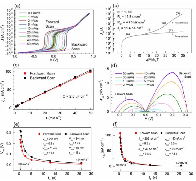
(22) to label such transient dark parameter as : the voltage at which the current density is zero in the dark curves. transient behavior can be observed by plotting its evolution with stabilization time .. (3.14). The resulting trends are those of figure 3.3e, where two mechanisms with two different relaxation times are identified. The curves were fitted to a double exponential (3.15) and the calculated characteristic times were of about a second for the fast process and around ten seconds for the slow one.. Figure 3.3: (a) curves at different scan rates as indicated with logarithmic scaled currents. (b) Normalized equilibrium current ( in (a)) in logarithmic scale as a function of voltage in | | dimentionless units; (A) forward leakage current region, (B) generationrecombination current region, (C) diffusion current region, (D) high-injection and seriesresistance effect region, and (E) reverse leakage current due to generation-recombination and surface effects. (c) Absolute capacitive currents at . (d) “Apparent” output power from curves of (a). Dark crossing axeses voltage (e) and current density (f) with respect to stabilization time.. 22.
(23) Interestingly, is more than the 70% of total amplitude . This means that for achieving steady-state curve, there are two different capacitive mechanisms, and in a range of scan rate the hysteresis will be appreciably decreased with . This range is characterized by the stabilization time . For those scan rates with a greater than stabilization time ( , the equilibrium condition will not be reached until . A similar analysis can be made with the current density at which the voltage is zero (see figure 3.3f) by fitting to an analogue double exponential decay. .. (3.11). The result seems to match with the same general tendency; however the times are slightly smaller. This can be interpreted if we consider that the transient changes in charge distribution make a faster contribution to the continuous current than to the field configuration into the device, that is, a displacement current delay the field response. Until here we have contribute with evidence about the capacitive nature of curve hysteresis by studying its behavior at different scan rate and bias sweep direction. Our experiments were performed in dark conditions and at room temperature. We have correlated such capacitive origin with displacement currents and as is expected with the dielectric constant of MAPI (see equation 3.5). It is known that the MAPI tetragonal structure ( -phase) changes to orthorhombic structure ( -phase) below 200 K.39,44,47,94 Such transition is reflected in the MAPI dielectric constant that experiments a step around the same range of temperature.62,94 Consequently, it is then expected that, if capacitive origins are taken into account, the curve hysteresis will “feel” the phase transition effect. In order to test such hypothesis, dark curves were measured in a range of temperatures from room to 130 K (figure 3.4a). The general shape of the curves appears not different than those of figure 3.3a while above 200 K. The current decreases with temperature, however the hysteretic behavior has not a clear trend. Below 200 K the curves collapse and the is significantly enhanced. In order to better appreciate such phenomenon figure 3.4b exhibits the difference between bias scan directions ( ) of and (left and right axis, respectively). It is evident how both parameters experiment a step in the temperature vicinity of the phase transition. Complementary impedance spectroscopy measurements were carried out for obtaining the MAPI relative dielectric constant at (figure 3.4c). Interestingly, increases as temperature does with the same general trend than the dielectric constant does, as is expected from displacement current originated effects (equation 3.2).. 23.
(24) Figure 3.4: (a) curves at different temperatures as indicated with logarithmic scaled currents; the voltage was sweept at . (b) Absolute difference between bias scan directions of and (left and right axis respectively) as a function of temperature. (c) Relative dielectric constant as a function of temperature from impedance spectroscopy at 100 kHz with a rugosity of 10 in the mesoporous TiO2 layer.. On the other hand, the exhibits a sharper step in the opposite direction. Among the possible origins for its augmentation with the decrease of temperature can be considered: (i) band gap enhancement in orthorhombic phase39 (ii) trapping shallow states carrier life time increment,95 or (iii) ferroelectric behavior.96 In summary, dark curves have evidenced capacitive features by exploring the linear behavior of capacitive currents as a function of bias scan rate and direction. A steady state dark curve was found at whose parameterization suggest larger recombination and leakage current influence. The observation of stabilization time profiles of and allowed to identify two different capacitive mechanisms, with different characteristic times in the order of seconds. The characterization was complementary performed at low temperatures below the MAPI transition phase, resulting that capacitive currents follows the step in dielectric constant measured by impedance spectroscopy.. 24.
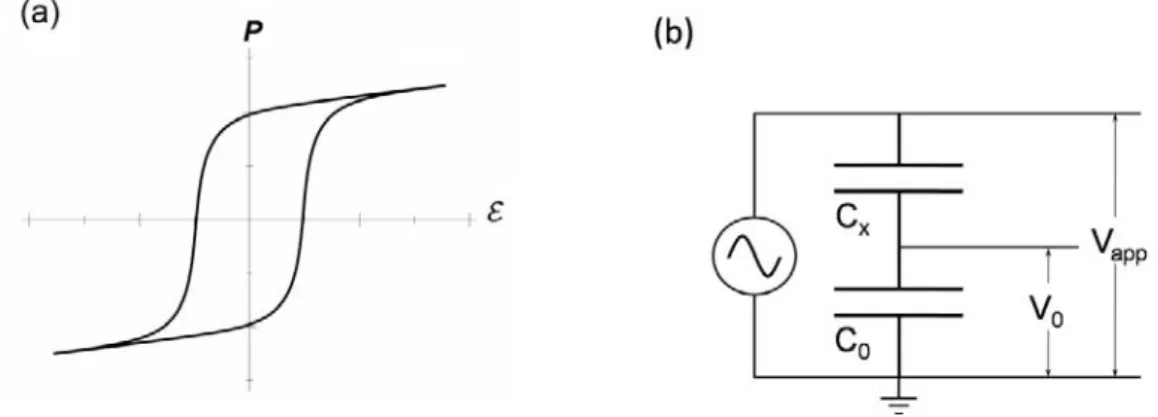
(25) 4. Sawyer-Tower circuit measurements Since the most studied family of ferroelectric materials has been the perovskite oxides,16,97 the identification of ferroelectric effect and the evaluation of its role in perovskite solar cells has focused a lot of attention. Furthermore, it has been among the most controversial issues during the development of these devices. As it was reviewed at the beginning of the previous chapter, several studies have contributed with evidence and/or hypothesizes for or against the ferroelectric explanation concerning the J-V curve hysteretic behavior. However, not conclusive proofs have been provided of its macroscopic impact in the electrical response of the MAPI. This may be mainly due to the thin film configuration in which the devices are often fabricated. It is known that thin films ferroelectrics are seldom perfectly resistive and the presence of grain boundaries, defects, or conduction processes such as tunneling, can allow significant leakage currents to exist. These circumstances can make it difficult to tell the difference between a sample that is simply a linear dielectric and one that is truly ferroelectric.16,97 Traditionally a capacitance bridge, as first described by Sawyer and Tower,98 is the used set up to obtain the characteristic ferroelectric hysteretic loops (figure 4.1a). The typical hysteresis loop arises when over certain field value the polarization saturates to the linear relation . The Sawyer-Tower circuit (STC) is shown in figure 4.1b. In such configuration a voltage signal is applied to the sample and a reference linear capacitor in series by mean of a sinusoidal (or triangular) wave generator. Thereupon the charge in (as in ) is , being the potential drop through the reference capacitor that is measured in an oscilloscope. is plotted on the Y-axis, and is plotted on the X-axis in the oscilloscope X–Y mode. The is made under the criterion of so that the potential across selection of should be small enough not to affect the potential across . The calculus of polarization is made as and the field is approximated to , where . Ideal ferroelectric samples produce a frequency is the plates separation in independent loop as figure 4.1a while pure linear dielectrics (capacitors) provide a straight line and pure resistive samples (resistors) give an ellipse (or a tilted rugby football shape, in the case of a triangular ).16,97-99. Figure 4.1: (a) Polarization-Field hysteresis loop of an ideal ferroelectric material. (b) Sawyer– Tower circuit sketch.. 25.
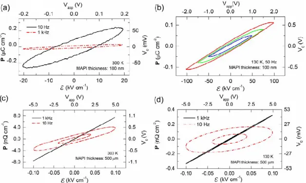
(26) In a first attempt for identify ferroelectric effect in complete devices, the STC measurements at room temperature resulted in the ellipses of figure 4.2a. Such sort of Lissajous figures are characteristic of equivalent resistor-capacitor (RC) circuits, with frequency dependent tilting (lessening of due to potential drop increase in the sample) and widening (phase shift between and ). These two characteristics are the effect of frequency dependent capacitance and resistivity which have been widely reported in the literature from impedance spectroscopy studies.51,61,62,74,75,100 Further measurements were made at lower temperatures seeking for possible ferroelectric features below the transition phase. However not different general trends were found. Interestingly, specifically at frequency and temperature of 50 Hz and 130 K, respectively, some nonlinearities arose giving a more similar to hysteretic loop shape (see figure 4.2b). Nevertheless, different applied fields were explored and saturation was not found. The profiles were like identically reproduced at different scales, which cannot be interpreted as a ferroelectric feature. Aiming to discard the undesired effects of thin film structure and selective contacts which are present in complete devices, MAPI pellets of diameter and thickness were also measured in the STC set up. Figures 4.2c,d resume the resulting profiles for different frequencies and at room and 130 K temperatures. The shapes are not too much different from ellipses and at larger frequencies straight lines were obtained, as pure capacitive responses.. Figure 4.2: Polarization-field profiles from STC measurements for different frequencies, temperature and MAPI thickness as indicated.. In summary, STC measurements were carried on MAPI thin film based solar cells and large crystals MAPI pellets and as result no proofs of ferroelectric behavior was found. Instead of typical hysteretic loop, a set of Lissajous figures frequency and temperature 26.
(27) dependent resulted, which is a characteristic RC equivalent circuit feature. The presence of some nonlinearities at some particular temperatures and frequencies can be associated to the MAPI frequency and temperature dependent impedance spectrum.. 27.
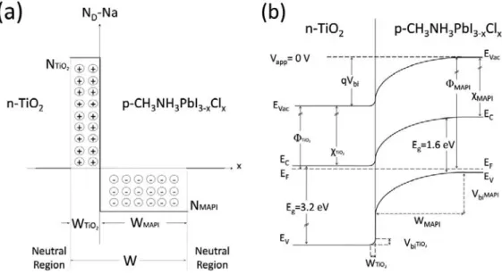
(28) 5. Capacitance-voltage characterization The PSCs p-n junction formation takes place when the p-type MAPI is intimately joined with the n-type TiO2. Hence two layers of uncompensated acceptors and donors, respectively, on either side of the junction form a dipole that holds the barrier by equalizing the Fermi levels. In the abrupt step junction approximation it result in a charge density profile like in figure 5.1a, where the positive charge is distributed in the , at the TiO2 side; the with a donor defect concentration depleted zone negative charge lies in the depleted zone with acceptor concentration , at the MAPI side; and elsewhere a neutral region is understood. The charge neutrality of is larger . Since the device has to be satisfied, so 76 than , the depletion region is mainly placed in the MAPI. By solving the Poisson equation with the boundary condition of the electric displacement vector continuity at the interface, the depletion zones widths can be obtained as a function of the total built-in potential : √. (. (5.1). ). and √. (. ). ,. (5.2). where is the TiO2 relative dielectric constant. Figure 5.1b displays the band diagram of the junction at zero applied potential, illustrating the band bending at each part of the interface. The is distributed between the partial built-in potential at the MAPI side, which is the larger one, and the partial built-in potential at the TiO2 side; i.e. . In addition, they are related to each other as .. (5.3). The TiO2 work function ( )101 and electron affinity ( )102 proximity indicates the strong n-type nature of the mesoporous scaffold. On the other hand; from earlier estimations of the MAPI work function ( ),103 electron affinity ( ),103 and bandgap ( );40,89,104,105 the p-type character of the absorber material is not so marked. Furthermore, bearing in mind that69,81 | the. |,. (5.4). value is expected to be around 1.0 V, as some works have already reported.. 76,106,107. 28.
(29) Figure 5.1: MAPI based solar cells (a) abrupt junction charge density profile69,71,77,78 and (b) energy band diagram.28,30,45,76,104,108 The draws are not scaled and trap levels contributions were neglected.. For the above described system we can define the depletion-layer capacitance per unit area as , where is the incremental depletion charge on each side of the junction (total charge is zero) upon an incremental change of the applied voltage . An expression for such capacitance is obtained by considering the heterojunction as a parallel plate capacitor filled by two different dielectrics one after the other (series connection). Hence, after the proper algebra can be presented in the form (. ). .. Typically, the one-side depletion junction is assumed ( and equation 5.5 can be reduced to the classic Mott-Schottky equation. (5.5) ,. ),. (5.6) where the effects of the n-side upon the band bending are neglected. Subsequently, from and , and the is equations 5.5,6 a linear dependency is expected between called the Mott-Schottky plot (MSP). Therefore is measured as a function of DC by impedance analysis and from the MSP slope and the intercept calculus the unknown parameters in equations 5.5,6 are evaluated. This procedure has been widely employed for characterizing PSCs, however mistaken performance or understanding of the experiment have been systematically done.73,78,79,100,107,109,110 Three important issues need to be taken into account in order to present a truthful Mott-Schottky analysis: (i) identification of the dipolar polarization frequency range in the capacitance spectrum, (ii) identification of the Mott-Schottky behavior in the MSP, (iii) consideration of n-side contributions to the model (use of equation 5.5 instead of equation 5.6). 29.
(30) Since the capacitance measurement is made by impedance spectroscopy,111 the selection of the AC signal frequency at which the DC voltage sweep is going to be performed is critical in the final MSP interpretation. As it has been recently pointed,62 the capacitance spectrum at room temperature presents three clear regions associated to different mechanism (figure5.2a). At low frequencies a capacitance excess arises possibly from electrode polarization and at the larger frequencies a transition to the high-frequency limit occurs. Between the two limits, a capacitance plateau lies for the dipolar polarization. There is where the MSP analysis must be carried. Therefore, the omission of (i) the capacitance spectra and (ii) the frequency specification should account for the nullification of a presented MSP analysis. On the other hand, assuming that the MSP impedance spectroscopy frequency has been well selected, still there is a common misunderstanding on PSCs Mott-Schottky procedure. Figure 5.2 stays for a general PSC MSP where three main regions are highlighted. In spite of other photovoltaic technologies like Si112,113 or CdTe72,114 where the curves are mainly placed in the reverse bias region, the PSCs experiments full depletion as quick as a few hundreds of reverse millivolts are reached. The irregularities of such regions can be associated with non-steady state interaction of the depletion layer boundary with the opposite MAPI interface (spiro-OMeTAD in our case). Consequently, DC applied potential must explore mainly the smaller than forward bias region in order to shrink the space charge, instead of enlarge it. Figure 5.2b displays such region in between zero and where the linear Mott-Schottky behavior is apparent. However, at larger than forward DC bias an exponential decrease of separates the MSP from the linear behavior (dashed lines). This presumably accounts for chemical capacitance predominance, where the linear fit must not be made. The mistaken assumption of the like-linear tail at the beginning of the exponential decay as Mott-Schottky behavior could be the reason why some relatively low have been 100,107,110 reported. Then it is also essential to support the MSP analysis with the respective logarithmic scaled curve, like figure 5.3a, where it is clear the change of capacitance response dominating mechanism by the variation of curve slope.. Figure 5.2: (a) Capacitance spectrum measured via impedance spectroscopy at zero DC voltage and (b) Mott-Schottcky plot for PSCs studied in this work.. The chemical capacitance, also known as diffusion capacitance (see figure 3.3b),69 arises from the voltage dependent rearrangement of minority carriers, instead of the 30.
(31) depletion region width change with the applied potential. As the forward bias increases, the space charge wanes, hence the interface of the heterojunction becomes in a more important role in the capacitance response. It is well known that the exponential DOS of the TiO2 below the conduction band results in the bandgap traps originated chemical capacitance per unit area81,111,112 ,. (5.7). where is the localized states layer width and can be still interpreted in terms of the ideality factor due to the proportional relation between and the forward current.69,112 Hence, it is feasible to associate the exponential capacitance increase at near flat band forward bias (figure 5.3a) with a DOS like in equation 5.7, despite its origin cannot be simply ascribed to TiO2 or/and MAPI. Furthermore, possible effects of parasitic low frequency capacitances should not be discarded in order to make a truthful interpretation of the PSCs capacitive characteristics. So far, we have introduced the fundamentals of capacitance-voltage characterization and the main features to take into account for accurate MSP analysis on PSCs. Thus, in the following we present our measurements of PSCs capacitance as a function of DC voltage at 1 kHz, where the bias swept was once more performed in both senses (figure 5.3) at an approximate scan rate of . Differently to experiments were no pre-treatment was applied, here the samples were previously set at and during minutes for FS and BS, respectively.. Figure 5.3: (a) Capacitance-voltage measurements at FS and BS measured by impedance spectroscopy at 1 kHz. Three main behaviors are pointed: (A) full depletion, (B) Mot-Schottky behavior, and (C) chemical capacitance dominance. The later is better viewed in the inset where resulting ideality factors are also displayed. (b) Mott-Schottcky plot at FS and BS with calculated parameters as indicated.. As indicated in logarithm scaled capacitance figure 5.3a, the three figure 5.2b pointed regions can be identified (capital letters) in both scan directions. In the inset the region is better observed and the respective ideality factors are also displayed. Interestingly, as from curve analysis, is larger at FS than at BS. Besides, figure 5.3b shows the corresponding MSPs that make apparent the different Mott-Schottky 31.
(32) behavior between scan senses. By using equations 5.1,2,5 and the TiO2 doping profile ) study results of A. Guerrero et al.,76 the heterojunction ( parameters were calculated and the values also displayed in figure 5.3b. It is worthy to remark that while the decrease around a 17% from FS to BS, just diminishes a 1.8%. In the first place, the former would not be understood in terms of the MAPI or TiO2 work function variation (equation 5.4). Instead, a dipole layer at the MAPI interfaces with a consequent vacuum level shift can be considered.81 Following that idea, we can rewrite equation 5.4 as |. |. (5.8). where is the dipole layer potential drop whose sign depends on the earlier mentioned displacement current sense and is the flat band potential. With this consideration the true value would be and . This dipole layer can be related to the earlier referred slow dynamic ions movement that directly affects the contact resistance at the interfaces producing the capacitive hysteresis in curves. On the other hand, the poor (or absent) space charge variation could suggest that the changes on recombination current ( ) should be associated rather to than . This can be checked by calculating from the linear trends of figure 5.3a inset and using equation 5.7. Here we must underline two important facts: (i) the voltage section in which the fitting is carrier must be the closer to flat band configuration ( ), and (ii) the uncertainty is estimated in an order of magnitude given that is calculated from the intercept of linear behaviors in logarithmic scale, hence small slope tilts result in magnitude orders changes. Taking that into account, the consequential calculated values result in more than two order of magnitude difference between BS and FS, being the last much greater than the first. One can think in mobile ionic charge that passivate the traps levels rather in BS than in FS. In addition, when we try to estimate where the localized states are distributed we find that it better suits with interface phenomena. If we take , then is and at FS and BS, respectively. These carrier density values are quite smaller than typical reports in literature ( ) for Si solar cells,112 TiO2 in DSCs,115 and nanostructured TiO2,111,116 where is often estimated in the order of micrometers. If these were bulk localized states in TiO2 or MAPI, then and hence , which is a situation that seems even more extreme. Summarizing, by a review of the state-of-the-art on Mott-Schottky plot analysis in MAPI based devices we found some irregularities in the measurements performance and graphs interpretation. Therefore, we here give a detailed methodological guide for its correct implementation in PSCs. Subsequently, we have presented our cells measurements and by exploring the capacitance-voltage characteristic at different DC voltage scan directions we found evidence of a dipole layer presumably placed at the MAPI interfaces. Furthermore, from the chemical capacitance exponential increase at 32.
(33) flat band condition we estimated the total density of trap localized states below the conduction band obtaining relatively low values whose distribution would be better placed in a thin layer at an interface.. 33.
(34) 6. Conclusions The perovskite solar cells electrical response is a fruitful field for researchers aiming to plenty understand the mechanisms that rules its behavior. Further investigation needs to be done in order to clarify the origins of the current density-voltage curve hysteresis and the capacitance excess at low frequencies in the spectrum from impedance spectroscopy. In the present work we have contributed with further evidence that proposes the connection of such issues as effects possibly caused by ionic charge accumulation at the perovskite interfaces behaving as capacitors. The CH3NH3PbI3-xClx based solar cells characteristics under illumination at different irradiances and bias scan direction were studied. It resulted in a possible light independent change in the recombination processes between scan directions; i. e. more recombination at forward than at backward scan. Dark curves for different scan rates were checked in the shunt resistance and recombination region and as result a text book capacitive linear trend with scan rate was found. Furthermore, a steady-state curve was achieved at and the stabilization time evolution of dark apparent parameters like showed characteristic life-times in the order of seconds. By changing temperatures, dark capacitive currents were tested to follow the dielectric constant behavior as displacement currents should do. In other experiment, Sawyer-Tower circuit measurements at different temperatures were carried, as much in CH3NH3PbI3-xClx based solar cells as in CH3NH3PbI3 pellets, looking for ferroelectric polarization-field loops and temperature and frequency dependent RC Lissajous figures were obtained. In order to further explore the capacitive features of the CH3NH3PbI3-xClx based solar cells, capacitance-voltage measurements were conducted with the complemented support of capacitance spectra from impedance spectroscopy. In this sense, a methodological guide was proposed for accurate Mott-Schottky plot analysis on PSCs. Subsequently, we found an exponential chemical capacitance increase in the diffusion region which could be related with an exponential density of trap localized states below the conduction band. The estimated total concentration of such localized states was relatively low, which suggest a possible localization at an interface. The capacitancevoltage measurements were made in both DC bias scan directions, and noticeable difference appeared. In the chemical capacitance prevailing region it resulted in more than two order of magnitude larger concentration of localized states at forward than at backward bias scan, when a sort of passivation process takes place. This is consequent with above conclusions of recombination dependence with scan direction. In addition, The Mott-Schottky plots showed a clear change of built-in potential. Such effect can be understood as a flat band modification produced by a dipole layer, in agree with previous proposals about capacitive displacement currents.. 34.
(35) References 1. "World Energy Resources. 2013 Survey", (World Energy Council, UK, 2013); "Key World Energy Statistics 2014", (OECD/IEA, Paris, France, 2014); "BP Statistical Review of World Energy", (2015).. 2. Monica Das Gupta, Robert Engelman, Jessica Levy, Gretchen Luchsinger, Tom Merrick, and James E. Rosen, "State of world population 2014", edited by Richard Kollodge (UNFPA, 2015).. 3. Joshua M. Pearce, "Photovoltaics - a path to sustainable futures," Futures 34 (7), 663-674 (2002).. 4. P. Friedlingstein, R. A. Houghton, G. Marland, J. Hackler, T. A. Boden, T. J. Conway, J. G. Canadell, M. R. Raupach, P. Ciais, and C. Le Quere, "Update on CO2 emissions," Nature Geosci 3 (12), 811-812 (2010).. 5. Luis Hernández, "El problema energético en el desarrollo global y la energía fotovoltaica," Revista Iberoamericana de Física 2 (1), 2-6 (2006).. 6. Theocharis Tsoutsos, Niki Frantzeskaki, and Vassilis Gekas, "Environmental impacts from the solar energy technologies," Energy Policy 33 (3), 289-296 (2005); Varun, Ravi Prakash, and Inder Krishnan Bhat, "Energy, economics and environmental impacts of renewable energy systems," Renewable and Sustainable Energy Reviews 13 (9), 2716-2721 (2009).. 7. D. M. Chapin, C. S. Fuller, and G. L. Pearson, "A New Silicon p‐n Junction Photocell for Converting Solar Radiation into Electrical Power," Journal of Applied Physics 25 (5), 676-677 (1954).. 8. Gaëtan Masson, Marie Latour, Manoël Rekinger, Ioannis-Thomas Theologitis, and Myrto Papoutsi, in Global market outlook for photovoltaics 2013-2017, edited by Craig Winneker (EPIA, 2013).. 9. A. Romeo, M. Terheggen, D. Abou-Ras, D. L. Bätzner, F. J. Haug, M. Kälin, D. Rudmann, and A. N. Tiwari, "Development of thin-film Cu(In,Ga)Se2 and CdTe solar cells," Progress in Photovoltaics: Research and Applications 12 (2-3), 93111 (2004).. 10. Michael Grätzel, "Dye-sensitized solar cells," Journal of Photochemistry and Photobiology C: Photochemistry Reviews 4 (2), 145-153 (2003).. 11. Harald Hoppe and Niyazi Serdar Sariciftci, "Organic solar cells: An overview," Journal of Materials Research 19 (07), 1924-1945 (2004).. 12. Martin A. Green, Keith Emery, Yoshihiro Hishikawa, Wilhelm Warta, and Ewan D. Dunlop, "Solar cell efficiency tables (version 42)," Progress in Photovoltaics: Research and Applications 21 (5), 827-837 (2013).. 13. Martin A. Green, Keith Emery, Yoshihiro Hishikawa, Wilhelm Warta, and Ewan D. Dunlop, "Solar cell efficiency tables (version 46)," Progress in Photovoltaics: Research and Applications 23 (7), 805-812 (2015).. 14. Henry J. Snaith, "Perovskites: The Emergence of a New Era for Low-Cost, High-Efficiency Solar Cells," The Journal of Physical Chemistry Letters 4 (21), 3623-3630 (2013).. 15. Francis S. Galasso, Structure, properties and preparation of perovskite-type compounds. (Pergamon Press Inc., UK, 1969). 35.
(36) 16. Physics of Ferroelectrics. A Modern Perspective. (Springer, Verlag Berlin Heidelberg, 2007).. 17. G. Srinivasan, E. T. Rasmussen, B. J. Levin, and R. Hayes, "Magnetoelectric effects in bilayers and multilayers of magnetostrictive and piezoelectric perovskite oxides," Physical Review B 65 (13), 134402 (2002).. 18. Z. Fang, K. Terakura, and J. Kanamori, "Strong ferromagnetism and weak antiferromagnetism in double perovskites: Sr2FeMO6 (M=Mo, W, and Re)," Physical Review B 63 (18), 180407 (2001).. 19. Yoshiyuki Inaguma, Jean-Marc Greneche, Marie-Pierre Crosnier-Lopez, Tetsuhiro Katsumata, Yvon Calage, and Jean-Louis Fourquet, "Structure and Mössbauer Studies of F−O Ordering in Antiferromagnetic Perovskite PbFeO2F," Chemistry of Materials 17 (6), 1386-1390 (2005).. 20. T. Okuda, K. Nakanishi, S. Miyasaka, and Y. Tokura, "Large thermoelectric response of metallic perovskites: Sr1-xLaxTiO3 (0<x<0.1)," Physical Review B 63 (11), 113104 (2001).. 21. H. Kumigashira, R. Hashimoto, A. Chikamatsu, M. Oshima, T. Ohnishi, M. Lippmaa, H. Wadati, A. Fujimori, K. Ono, M. Kawasaki, and H. Koinuma, "In situ resonant photoemission characterization of La0.6Sr0.4MnO3 layers buried in insulating perovskite oxides," Journal of Applied Physics 99 (8), 08S903 (2006).. 22. N. N. Toan, S. Saukko, and V. Lantto, "Gas sensing with semiconducting perovskite oxide LaFeO3," Physica B: Condensed Matter 327 (2–4), 279-282 (2003).. 23. K. P. Rajeev, G. V. Shivashankar, and A. K. Raychaudhuri, "Low-temperature electronic properties of a normal conducting perovskite oxide (LaNiO3)," Solid State Communications 79 (7), 591-595 (1991).. 24. S. Y. Li, R. Fan, X. H. Chen, C. H. Wang, W. Q. Mo, K. Q. Ruan, Y. M. Xiong, X. G. Luo, H. T. Zhang, L. Li, Z. Sun, and L. Z. Cao, "Normal state resistivity, upper critical field, and Hall effect in superconducting perovskite MgCNi3," Physical Review B 64 (13), 132505 (2001).. 25. Akihiro Kojimaa, Kenjiro Teshimad, Yasuo Shiraic, and Tsutomu Miyasaka, Novel Photoelectrochemical Cell with Mesoscopic Electrodes Sensitized by Lead-halide Compounds (11) (Cancun, Mexico, 2006).. 26. Akihiro Kojima, Kenjiro Teshima, Yasuo Shirai, and Tsutomu Miyasaka, "Organometal Halide Perovskites as Visible-Light Sensitizers for Photovoltaic Cells," Journal of the American Chemical Society 131 (17), 6050-6051 (2009); Jeong-Hyeok Im, Chang-Ryul Lee, Jin-Wook Lee, Sang-Won Park, and Nam-Gyu Park, "6.5% efficient perovskite quantum-dot-sensitized solar cell," Nanoscale 3 (10), 4088-4093 (2011).. 27. Hui-Seon Kim, Chang-Ryul Lee, Jeong-Hyeok Im, Ki-Beom Lee, Thomas Moehl, Arianna Marchioro, Soo-Jin Moon, Robin Humphry-Baker, Jun-Ho Yum, Jacques E. Moser, Michael Grätzel, and Nam-Gyu Park, "Lead Iodide Perovskite Sensitized All-Solid-State Submicron Thin Film Mesoscopic Solar Cell with Efficiency Exceeding 9%," Scientific Reports 2, 591 (2012).. 28. Michael M. Lee, Joël Teuscher, Tsutomu Miyasaka, Takurou N. Murakami, and Henry J. Snaith, "Efficient Hybrid Solar Cells Based on Meso-Superstructured Organometal Halide Perovskites," Science 338 (6107), 643-647 (2012). 36.
Figure


+7
Documento similar