Pulsed Current Source with Active Control of the
On-Time Current for LED Lamp Driver Applications
C. Brañas, F. J. Azcondo, R. Casanueva, F. J. Díaz
University of CantabriaElectronics Technology, Systems and Automation Engineering Department Ave. de los Castros s/n 39005 Santander, SPAIN
[email protected] Abstract -This paper presents a simplified envelope model to
study the dynamics of a phase-controlled resonant converter suitable to drive light emitting diode (LED) lamps. The approximate closed form of the transfer function is obtained from the proposed reduced-order model. The fast dynamics of the resonant converter allows us implementing a pulsed current source with active control of the on-time-current free of instabilities and flicker effect with a type II or integral-single-lead controller. A 120W prototype intended for street lighting applications has been built to validate the study.
Index Terms – Light sources, LED lamps, lighting control, feedback circuits, negative feedback, close loop systems, phase shifters.
I. INTRODUCTION
In order to prevent the degradation of the LED light quality parameters, it is recommendable to operate the LEDs at their nominal current [1]. For this reason, the dimming is generally implemented turning on/off the nominal LED current, according to a PWM pattern, modifying only the average current while preserving its amplitude. A fast response in the LED current control is required to achieve PWM dimming operation at a frequency above 200Hz to prevent the imperceptible flickering effect [2].
This paper analyzes the dynamic response of a phase-controlled series-parallel resonant converter. Different models have been proposed to study the dynamic response [3-4] of resonant converters. In general, the small signal modeling of resonant converters is a complex task, taking into account the number of reactive elements and operation modes. In this paper, to deal with the complexity of the full order system, a reduced-order model of an equivalent LCp network is derived.
Using the reduced order model, the closed form of the control-to-output transfer function is obtained. The main frequency limitation takes place at the output filter of the converter, although the bandwidth is wide enough to achieve PWM dimming control at 500Hz while preserving the active control of the on-time-current by using an integral-single-lead controller.
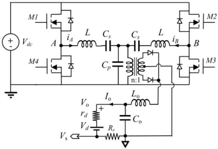
II. PHASE CONTROLLED LCSCPRESONANT CONVERTER The phase-controlled LCsCp converter [5] (Fig. 1) consist of
two stages: the resonant inverter loaded by a center tap rectifier with an output filter. The step down transformer with ratio n:1 provides galvanic insulation. The LED array is connected on the DC side, at the output of the center tap rectifier and is
represented by the linear model of the diode, so that
Vo=rdIo+Vd.
Fig. 1. Phase-controlled LCsCp resonant inverter
Considering that the output filter is well designed, it removes the high frequency ripple due to the inverter stage operation thus, the rectifier section can be modeled at low frequency by using averaged values [6]. Using the first harmonic of a square waveform, the relationship between the AC and DC side currents is given by,
ac o I n I ˆ 4 ⋅ = π (1)
On the other hand, the voltage of the LED lamp, Vo, is
obtained as the mean value of the full wave rectified voltage.
d o d ac o V r I V n V = 2 ⋅ˆ = ⋅ + π (2)
From (1) and (2), the lamp model is represented in the AC side by, d ac d ac V n I r n V = ⋅ + ⋅ 2 ˆ 8 ˆ 2π2 π (3)
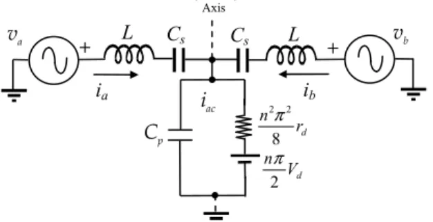
Once the load is transferred to the AC side, the fundamental approximation [2] is applied for the circuit analysis. The mid-point voltages va and vb in Fig. 2 are represented by complex
phasors, ) 2 ( 2 , = ⋅ ± Ψ j e Vdc B A π V , (4)
where Ψ is the phase displacement between va and vb.
M2 M1 M4 iA A B Cp L M3 L Cs i B n:1 Lo Co Io Rs Cs rd Vd + Vo Vs Vdc
+-Fig. 2. Simplified circuit for steady-state analysis purposes.
For nominal conditions, the impedance seen from the AC side, Rac, considering the continuous conduction mode of the
rectifier stage [6] is,
o ac n R R 2 2 8 π = , (5)
where Ro is the DC equivalent impedance of the LED array, Ro=Vo/Io=rd+Vd/Io. The parallel parameters of the LCsCp
inverter are summarized in Table I.
p p p p C L Z ω ω = 2 = 2 1 p p LC = ω p ac p Z R Q =2 Parallel Resonant Frequency Parallel Characteristic Impedance Parallel Quality Factor TABLE I.
PARAMETERS OF THE LCsCpINVERTER
Since LEDs are current-driven devices, current source behavior of the driver circuit is highly desirable. For the LCsCp
resonant inverter, the current source behavior is found at ωo,
where the switching frequency, Ωo is set.
s p p o o= = 1+C 2C Ω ω ω , (6)
The amplitude of the output current in the converter AC side, given at ω=ωo is calculated according to (4).
( )
2 2 1 4 ˆ = + CosΨ Z C C V I p s p dc ac π , (7)From (7) it can be observed that Îac can be adjusted, at
constant switching frequency, by the phase displacement angle, Ψ, being the control parameter. Since the LED array is connected on the DC side, upon substitution of (7) into (1), the DC output current is obtained as a function of the inverter parameters:
( )
2 2 1 Ψ + = Cos Z C C nV I p s p dc o . (8) A. Converter DesignThe lamp consists of four Bridgelux BXRA-C2000 LED arrays with a nominal current of Io=1.75A. Considering the
series connection of four arrays, the total output power is
Po=120W and the output voltage is Vo=68.6V, the equivalent
DC load being Ro=39.2Ω. In order to provide full control
capability, the control angle at nominal conditions is fixed at Ψo=45º. The input DC voltage is Vdc=400V, supplied by a PFC
stage. The transformer turns ratio is chosen to be n=2, which implies that Rac=193Ω. The capacitor ratio is Cp/Cs=0.1. Upon
substitution the design data into (8), the characteristic impedance is obtained, Zp=433Ω. The switching frequency is
set at Ωo=2π(100kHz). The parallel resonant frequency is determined from (6), ωp=2π(97.6kHz). Finally, the reactive
components are obtained, L=705μH, Cp=7.5nF and Cs=75nF.
The output filter components are Lo=1mH and Co=3.3μF.
III. REDUCED ORDER ENVELOPE MODEL OF THE PHASE -CONTROLLED LCSCPRESONANT INVERTER
The circuit in Fig. 2 exhibits a symmetrical structure, where the symmetry axis is defined by the ground-connected load. For this type of network, the bisection theorem enables the study of the circuit by using only one half of the whole circuit. Carrying out the decomposition of input voltages VA and VB in
(4) into their orthogonal components, it is observed that the imaginary parts of phasors VA and VB have equal amplitude
and 180º phase displacement, therefore they are cancelled out
) 2 ( 2 ) 2 ( 2 ,B dc o dc o A Sin V j Cos V Ψ ⋅ ± Ψ ⋅ = π π V . (9)
In this way, the resonant inverter is reduced to the equivalent circuit, shown in Fig. 3, where the input voltage is the real part of VA and VB (pure common-mode voltage).
Fig. 3. Phase-controlled LCsCp resonant inverter. Circuit simplified according
the bisection theorem.
A. Envelope Model
During operation, the resonant converter is affected by low frequency events, namely perturbations. The variation of the waveforms' amplitude provides useful information of the resonant converter dynamics. Using the phasor transformation method as introduced in [7], the time-varying amplitude current and voltage phasors are defined according to (10) and (11), taking into account that the switching frequency of the converter is constant, ω=ωο=Ωο, ] ) ( Re[ ) (t I t ej ot i = ⋅ Ω (10) ] ) ( Re[ ) (t V t ej ot v = ⋅ Ω (11)
Upon substitution of (10) and (11) into the inductor voltage equation, the envelope model of the inductor is obtained [6].
+ Iab L Cp/2 Iac d r n 4 2 2π d V n 2 π Cs
(
2)
2 Ψ = VdcCos AB π V va + ia ib vb + L L Cp iac Symmetry Axis d r n 8 2 2π d V n 2 π Cs Cs) ( ) ( ) ( j LI t V t dt t I d L + Ωo = (12)
The direct translation into a circuit model of (12) is an inductor in series with an imaginary resistor. At the same time, the envelope model of the capacitor is obtained as a capacitor in parallel with an imaginary resistor. The imaginary resistor represents the steady-state impedance of the corresponding reactive element at the switching frequency. On the other hand, considering variable operation conditions, the control angle, Ψ, is time dependent, modifying the amplitude of the input voltage. t j dc ab e o t Cos V t v ⋅ Ω ⎥ ⎦ ⎤ ⎢ ⎣ ⎡ ⎟ ⎠ ⎞ ⎜ ⎝ ⎛Ψ =Re 2 2() ) ( π (13)
Therefore, the voltage source applied to the envelope model is given by, ⎟ ⎠ ⎞ ⎜ ⎝ ⎛Ψ = 2 ) ( 2 ) (t V Cos t V dc ab π . (14)
The envelope model of the LCsCp resonant circuit is obtained
in Fig. 4,
Fig. 4. Large-signal envelope model of the series-parallel resonant circuit.
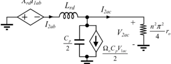
B. Reduced-Order Envelope Model
The calculation of the closed form of any transfer function using the envelope model of the series-parallel resonant circuit requires laborious mathematical work. Under the assumption that the switching frequency Ωo is much higher than the frequency band in which Ψ, and then the envelopes are perturbed, the model of capacitor Cs can be transformed [7]
into an equivalent inductor in series connection with the steady-state impedance as follows,
(15) s o o s s o s o s o j C sL C j C s C j s ⎟⎟⎠ + Ω ⎞ ⎜⎜ ⎝ ⎛ Ω ≈ Ω + Ω ≈ Ω + 1 1 ) ( 1 2 2 ω ,
where, ωs, is the resonant frequency of the series branch L-Cs. s s LC 1 = ω (16)
After grouping terms, the envelope model of the series branch is reduced to an inductance, Lrd in series with an imaginary
resistor, jXrd, defined as follows:
⎥ ⎥ ⎦ ⎤ ⎢ ⎢ ⎣ ⎡ ⎟⎟ ⎠ ⎞ ⎜⎜ ⎝ ⎛ Ω + = 2 1 o s rd L L ω , (17) ⎥ ⎥ ⎦ ⎤ ⎢ ⎢ ⎣ ⎡ ⎟⎟ ⎠ ⎞ ⎜⎜ ⎝ ⎛ Ω − Ω = 2 1 o s o rd L X ω (18)
In this way, the model shown in Fig. 4 is simplified as can be seen in Fig. 5.
Fig. 5. Large-signal reduced-order envelope model of the proposed phase-controlled LCsCp resonant inverter.
It should be noted that the reduced-order model incorporates the main dynamic effect of capacitor Cs at low frequency,
which is expressed by the new inductor Lrd of the model. Using
this approximation, the dynamic behavior of the phase-controlled LCsCp inverter can be study through the envelope
model of the parallel Lrd-Cp/2 circuit with a high degree of
accuracy in the frequency range of interest.
From the analysis of the reduced-order envelope model shown in Fig. 5, the following parameters are defined as a function of the parallel parameters of the original circuit.
2 ) ( 1 ⎟⎟ ⎠ ⎞ ⎜⎜ ⎝ ⎛ Ω + = o s p r p ω ω ω (19) 2 ) ( 1 ⎟⎟ ⎠ ⎞ ⎜⎜ ⎝ ⎛ Ω + ⋅ = o s p r p Z Z ω (20) 2 ) ( 1 ⎟⎟ ⎠ ⎞ ⎜⎜ ⎝ ⎛ Ω + = o s p r p Q Q ω (21)
C. Real and Imaginary Subcircuits
The envelope model in Fig. 5 can be analyzed in terms of separate circuits, corresponding to the real and imaginary part of the complex model. According to the procedure explained in [8], all current and voltages are decomposed into its real and imaginary parts so, V=V1+jV2 and I=I1+jI2. After grouping
terms, the circuits, which model the real and imaginary parts, are shown in Figs. 6 and 7.
Fig. 6. Real part of the large-signal reduced-order envelope model.
o r n 4 2 2π d V n 2 π + Lrd ) (t VAB ab I jXrd +-p oC jΩ 2 2 p C ac I ) ( 2 I t n ac π Io ro Vd L ) (t VAB ab I Cs s oC jΩ 1 L jΩo + -p oC jΩ 2 2 p C ac I ro n 4 2 2π d V n 2 π + ) ( 2 I t n ac π Io ro Vd Lrd XrdI2ab ) (t VAB I1ac I1ab 2 2ac p oCV Ω 2 p C +- ro n 4 2 2π d V n 2 π V1ac +
-Fig. 7. Imaginary part of the large-signal reduced-order envelope model. The envelope of the output current in the AC side is reconstructed from its orthogonal components by applying (22). 2 2 2 1 ) ( ac ac ac t I I I = + (22)
Solving for frequency zero the envelope model of Fig. 5, the steady-state components of the output current, I1ac and I2ac, are
obtained. The value of each component, normalized with the steady-state output current amplitude is given by (23) and (24), where the factor m is given by (25)
2 ) ( ) ( 2 2 2 ) ( 2 ) ( 1 1 1 ⎟ ⎟ ⎠ ⎞ ⎜ ⎜ ⎝ ⎛ Ω + ⎥ ⎥ ⎦ ⎤ ⎢ ⎢ ⎣ ⎡ ⎟ ⎟ ⎠ ⎞ ⎜ ⎜ ⎝ ⎛ Ω ⋅ − ⎟ ⎟ ⎠ ⎞ ⎜ ⎜ ⎝ ⎛ Ω ⋅ − = r p r p o r p o r p o ac ac Q m m m I I ω ω ω (23) 2 ) ( ) ( 2 2 2 ) ( ) ( ) ( 2 1 ⎟⎟ ⎠ ⎞ ⎜ ⎜ ⎝ ⎛ Ω + ⎥ ⎥ ⎦ ⎤ ⎢ ⎢ ⎣ ⎡ ⎟ ⎟ ⎠ ⎞ ⎜ ⎜ ⎝ ⎛ Ω ⋅ − Ω ⋅ − = r p r p o r p o r p r p o ac ac Q m m Q m I I ω ω ω (24) ⎥ ⎥ ⎦ ⎤ ⎢ ⎢ ⎣ ⎡ ⎟⎟ ⎠ ⎞ ⎜⎜ ⎝ ⎛ Ω + ⎥ ⎥ ⎦ ⎤ ⎢ ⎢ ⎣ ⎡ ⎟⎟ ⎠ ⎞ ⎜⎜ ⎝ ⎛ Ω − = 2 2 1 1 o s o s m ω ω (25)
D. Small-Signal Envelope Model
As can be deduced from Fig. 5, the large-signal envelope model is a linear model [8]. In order to obtain the small-signal model, only the input voltage, which is a function of the control parameter, Ψ, has to be linearized by adding the small-signal variation, φ: φ + Ψ = Ψ o . (26) Substituting (26) into (14), ⎟ ⎠ ⎞ ⎜ ⎝ ⎛Ψ + ⋅ = +ˆ 2 cos 2 φ π o dc ab AB V v V
.
(27)Separating the small-signal component from operating point:
⎟ ⎠ ⎞ ⎜ ⎝ ⎛Ψ ⋅ ⋅ − = 2 sin ˆ dc o ab V v π φ
.
(28)The load is linearized in (29) according to the linear model of the diode and taking into account the shunt resistor Rs. Then, ro=rd+Rs where rd is the dynamic resistance of the LED array.
o ac n r r 2 2 8 π = , (29)
The small-signal reduced-order model of the phase-controlled
LCsCp resonant converter is shown in Fig. 8.
Fig. 8. Small-signal of the reduced-order envelope model. The small-signal transfer function from the control to the load current envelope is obtained by linearizing [9] the envelope obtained from (22): ⎟⎟ ⎠ ⎞ ⎜⎜ ⎝ ⎛ ⋅ + ⋅ ⋅ = ac ac ac ac ac ac ac I i I i I I iˆ φ 1 ˆ1 2 ˆ2 . (30)
In (30) î1ab and î2ab are the small-signal increments of I1ab and I2ab. From the small-signal model of the Lrd-Cp/2 circuit, shown
in Fig. 9, the phasor of the increment of the load current is obtained: (31)
( )
(
) (
)
1 1 2 2 ˆ ) ( ) ( 2 ) ( 2 + Ω + + Ω + ⋅ ⎟ ⎠ ⎞ ⎜ ⎝ ⎛Ψ ⋅ − = r p d p o r p o ac o dc ac Q j s j s r Sin V s i ω ω π φ ,where Qp(d) is defined taking into account the dynamic load
impedance, ) ( ) ( 2 r p ac d p Z r Q = . (32)
Splitting (31) into real and imaginary parts, the small-signal increments î1load and î2load are calculated. Upon substitution of
(23), (24), î1load and î2load into (30) the control-to-output current
transfer function in the AC side is obtained in (39). Solving the characteristic equation in (39) it yields two pairs of complex conjugates poles. These poles are calculated according to:
o d p d p r p d p r p p Q Q Q jm s =− + − 2 ± Ω ) ( ) ( ) ( ) ( ) ( 2 , 1 2 2 1 4 ω ω . (33) o d p d p r p d p r p p Q Q Q j s =− − − 2 ± Ω ) ( ) ( ) ( ) ( ) ( 4 , 3 2 2 1 4 ω ω . (34)
The frequency response of the resonant inverter stage is defined by ΩLF, which is calculated from the low frequency
poles given by (33) as,
ac i n ˆ 2 π îo ro Co Lo Lrd jXrd p oC jΩ 2 2 p C îab ⎟ ⎠ ⎞ ⎜ ⎝ ⎛Ψ ⋅ ⋅ − = 2 ˆ dc o ab Sin V v π φ o r n 4 2 2π ac vˆ+ - îac Lrd XrdI1ab I2ac I2ab 2 1ac p oCV Ω 2 p C ro n 4 2 2π V2ac + -
2 2 2 ) ( 2 ) ( 2 ) ( 2 4 1 1 o d p d p r p LF Q m Q Ω + ⎟ ⎟ ⎠ ⎞ ⎜ ⎜ ⎝ ⎛− + − = Ω ω . (35)
However, the dynamics of the resonant inverter stage [9] is attenuated by the output filter due to it imposes a dominant-pole which governs the frequency response of the resonant converter. From the circuit in Fig. 8, the transfer function (36) is obtained.
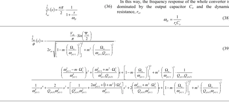
( )
H ac o s n s i i ω π + ⋅ = 1 1 2 ˆ ˆ (36)The frequency response of the whole converter is obtained from the convolution of (36) and (39), where at low frequency, the resonant inverter stage can be represented by an essentially flat gain, Φo, resulting from evaluating (39) for s→0.
H o ac ac o o s n i i i i ω π φ φ = ⋅ ≈ 2 ⋅1+Φ ˆ ˆ ˆ ˆ (37)
In this way, the frequency response of the whole converter is dominated by the output capacitor Co and the dynamic
resistance, ro. o o H C r 1 = ω (38)
( )
(
)
2 ) ( ) ( 2 2 2 ) ( 3 ) ( ) ( 2 2 2 ) ( 2 4 ) ( 2 2 2 ) ( 2 ) ( 2 ) ( 3 3 ) ( ) ( 4 4 ) ( ) ( ) ( 2 ) ( 2 2 2 ) ( ) ( 3 ) ( 2 2 2 ) ( 2 4 ) ( 2 2 ) ( 2 ) ( ) ( 2 2 2 ) ( 1 2 1 2 1 2 1 1 1 1 2 2 ˆ ⎟ ⎟ ⎠ ⎞ ⎜ ⎜ ⎝ ⎛ Ω ⋅ + ⎥ ⎥ ⎦ ⎤ ⎢ ⎢ ⎣ ⎡ ⎟ ⎟ ⎠ ⎞ ⎜ ⎜ ⎝ ⎛ Ω ⋅ − + ⎟ ⎟ ⎠ ⎞ ⎜ ⎜ ⎝ ⎛ + ⋅Ω + ⎥ ⎥ ⎦ ⎤ ⎢ ⎢ ⎣ ⎡ + + ⋅Ω + + + ⋅ ⎟ ⎟ ⎠ ⎞ ⎜ ⎜ ⎝ ⎛ Ω ⋅ + ⎥ ⎥ ⎦ ⎤ ⎢ ⎢ ⎣ ⎡ ⎟ ⎟ ⎠ ⎞ ⎜ ⎜ ⎝ ⎛ Ω ⋅ − + ⎟ ⎟ ⎠ ⎞ ⎜ ⎜ ⎝ ⎛ + ⋅Ω + ⎟ ⎟ ⎠ ⎞ ⎜ ⎜ ⎝ ⎛ − ⋅Ω ⋅ ⎟ ⎟ ⎠ ⎞ ⎜ ⎜ ⎝ ⎛ Ω ⋅ + ⎥ ⎥ ⎦ ⎤ ⎢ ⎢ ⎣ ⎡ ⎟ ⎟ ⎠ ⎞ ⎜ ⎜ ⎝ ⎛ Ω ⋅ − ⎟ ⎠ ⎞ ⎜ ⎝ ⎛Ψ ⋅ − = r p d p o r p o r p d p o r p r p o r p r p d p r p d p r p d p r p r p o r p o d p r p o r p r p o r p r p r p o r p o ac o dc ac Q m m s Q m s m Q s Q s Q Q m m s Q m s m Q m m r Sin V s i ω ω ω ω ω ω ω ω ω ω ω ω ω ω ω ω ω π φ (39) V EXPERIMENTAL RESULTSThe dynamic resistance of the LED lamp is: rd=6Ω. The
shunt resistor is Rs=0.5Ω, so the dynamic output resistance is ro=6.5Ω. Considering an output capacitor Co=3.3μF, the
theoretic bandwidth of the control-to-output transfer function is
ωH=2π(7.4kHz). The parameters of the reduced-order model
are: Lrd=738μH, Xrd=422Ω, ωp(r)=2π(95.3kHz), Zp(r)=443Ω,
Qp(r)=0.872, rac=32Ω, Qp(d)=0.145, m=0.909, Φo=-115.6mA/rad
and ΩLF=2π(92.1kHz).
The phase modulator was implemented using an isosceles-triangle carrier, a comparator and two monostable multivibrators. The waveforms are shown in Fig. 9
.
Fig. 9. Waveforms of the phase modulator with isosceles-triangle carrier.
The control voltage, vˆ , and the carrier are compared c
generating a PWM signal, which triggers both monostables, one of them with the positive edge and the other with the negative edge. In this way, drive signals of legs A and B of the converter are generated with a phase displacement adjusted according to the control action, vˆc.
The AC characterization, shown in Fig. 10, was carried out at constant amplitude, between 51.2 Hz and 51.2 kHz by using the Agilent 35670A Dynamic Signal Analyzer.
Fig. 10. Experimental AC response (red line) of the converter and theoretical (blue line) predicted by the proposed model.
In Fig. 10 it is considered that the response, iˆo, is measured on Rs resulting in vˆ and the gain of the phase modulator is s
constant [10], being Gφ=-0.95 rad/V so, the experimental result is plotted according to (40). ⎥ ⎦ ⎤ ⎢ ⎣ ⎡ ⋅ ⋅ ⋅ = ⎥ ⎦ ⎤ ⎢ ⎣ ⎡ φ φ R G î v v s o dB c s 20log ˆ ˆ (40)
From Fig. 10, it can be observed that the proposed model and the experimental results are in good agreement. The phase response of the experimental prototype has a higher value than the predicted by the model. The discrepancy is 20º at 10kHz. This deviation is caused by unmodeled delays in the path of the control signal, mainly due to the triangular phase modulator and dead time of the drivers of the MOSFETs. Despite of the phase increment, the first order nature of the converter makes the controller design easy achieving a good phase margin
ϕm=80º at a crossover frequency of ωc=2π(10kHz) by using a
Type II or integral-single-lead controller. The parameters of this controller have been set to: gain at ωc, Gc(ωc)=20dB, with
a zero at ωz=2π (2.68kHz) and pole at ωp=2π (37.32kHz).
The 500Hz PWM of the lamp current is achieved by imposing Ψ=180º, as can be seen in Fig. 11, in order to cancel out the output current Io.
Fig. 11. Signal command (Ch1) and midpoints voltages vA (Ch2) and vB
(Ch3) for phase-shifted PWM operation mode.
Fig. 12. Converter response for a duty cycle D=8%. Ch1: Signal command. Ch3: Lamp current. M: Lamp power.
During the on-time, Ψ is adjusted by the control-loop, setting up the nominal LED current Io=1.75A. The control-loop is fast
enough to set the nominal LED current operation even at values of duty cycle as low as D=8%, as can be seen in Fig. 12, where the LED current switches from cero to nominal conditions in 109μs.
CONCLUSIONS
The phase-controlled two-phase LCsCp resonant converter has
been proposed as a driver for LED lamps. The converter is designed as a current source. The output current is controlled, at constant switching frequency, through the phase displacement, Ψ, of the control signals of each inverter leg. The dimming control is achieved by operating the converter in phase-shift PWM mode. The dynamic study of the converter is in good agreement with experimental results. The phase-shift PWM mode provides a fast dynamic response of the converter, which allows the closed loop control operation at narrow duty cycles and implementing PWM dimming frequency high enough to prevent any flicker perception.
ACKNOWLEDGEMENT
This work is sponsored by the Spanish Ministry of Science and the EU through the project CICYT-FEDER- TEC2011-23612: “Power conversion with new digital control techniques and soft-saturation magnetic cores”.
REFERENCES
[1] Wai-Keung Lun, et al., “Implementation of Bi-level Current Driving Technique for Improved Efficacy of High-Power LEDs”. Energy Conversion Congress & Expo (ECCE), San Jose, CA, September 20-24, 2009. pp. 2808-2814.
[2] A. Wilkins, J. Veitch and B. Lelman, “LED Lighting Flicker and Potential Health Concerns: IEEE Standard PAR1789 Update” ECCE 2010, Atlanta, Georgia, September 12-16, pp. 171-178.
[3] Sanbao Zheng, Dariusz Czarkowski, “Dynamics of a Phase-Controlled Series-Parallel Resonant Converter”, IEEE Symposium on Circuit and Systems, 2002. (ISCAS2002), Vol.3. pp. 819-822.
[4]- Witulski, A.F.; Hernandez, A.F.; Erickson, R.W., “Small signal equivalent circuit modeling of resonant converters”, IEEE Trans on Power Elect., Vol. 6. No. 1 Jan. 1991. pp. 11–27.
[5]- D. Czarkowski, M.K. Kazimierczuk, "Phase-Controlled Series-Parallel Resonant Converter," IEEE Trans. on Power Elect., Vol.8, No.3, July 1993. pp. 309-319.
[6]- R. L. Steigerwald, “A Comparison of Half-Bridge Resonant Converter Topologies”, IEEE Trans. on Power Electronics, Vol. 7, No. 2, January 1992, pp. 89-98.
[7]- C.T. Rim, G.H. Cho, “Phasor Transformation and its Application to the dc/ac Analyzes of Frequency Phase-Controlled Series Resonant Converters (SRC)”, IEEE Trans. on Power Electron. Vol5, pp. 201-211, April 1990.
[8]- S. Lineykin and S. Ben-Yaakov, “Unified SPICE Compatible Model for Large and Small-Signal Envelope Simulation of Linear Circuits Excited by Modulated Signals”, IEEE Trans. on Ind. Electron., Vol. 53, No.3, pp. 745-751, June 2006.
[9]- Y. Yin, R. Zane, J. Glaser, R.W. Erickson, “Small-Signal Analysis of Frequency-Controlled Electronic Ballast”, IEEE Trans. on Circuit and Systems-I: Fund. Theory and Appl., Vol. 50, No.8, August 2003, pp. 1103-1110.
[10]- Luca Scandola, Luca Corradini and Giorgio Spiazzi, “Small-Signal Modeling of Uniformly Sampled Phase-Shift Modulators”, Proceedings of the 15th IEEE Workshop on Control and Modeling for Power
Electronics (COMPEL2014). June 22-25, 2014. Santander, Spain. 120W