UNIVERSIDAD DE CANTABRIA
Departamento de Ingeniería de Comunicaciones
TESIS DOCTORAL
Low Noise Receivers for Millimetre-wave Bands
Radio Astronomy
Receptores de Bajo Ruido para Radioastronomía en
Bandas de Ondas Milimétricas
Autor: José Vicente Terán Collantes
Directores: Eduardo Artal Latorre
Tesis doctoral para la obtención del título de Doctor por la Universidad
de Cantabria en Tecnologías de la Información y Comunicaciones en
Redes Móviles
Dedicado A la memoria de Carmen Collantes Fernández, Mi luz en el cielo.
Acknowledgments
To my family, Papa, Mama and Luisja. Their support and love show me the way to be better every day. And for give me the opportunity to have a University education. I wish to thank people from the Department of Communications Engineering of the University of Cantabria, professors Eduardo Artal and Maria Luisa de la Fuente for being my guide during the PhD and transfer me all their knowledge and experience. To all my colleagues Beatriz Aja, Juan Luis Cano, Eva Cuerno, Ana Rosa Pérez, and Enrique Villa for their assistance with all the work done, from Friday’s brain storming to coffee times. I remember all my University colleagues, from the first year in “Ingeniera Técnica” in 2001. They walked with along my University life. Special mention to Rubén Cavaducas, Jaime James, and David Güelu Bolucas. They converted into my friends and share special moments out the University, enjoying Verbenas parties, music festivals, and the passion for the mountains. In the end, we share Putas risas.
I wish to thank Rome, my lovely city. My work at University of Tor Vergata was so rewarding. The friendship of Xavi, Antonio, Helena, Susana, Carlos with our Sgroppino, Prosecco, and Peroni nights discovering the city and incredible places.
To Emma because you showed me the meaning of real and true love.
Oscarin, Pajarelis, the night fighters. You know your friendship and blessed madness will be with us forever. My Rabucas, Samu, Adri, Sara, Ana, Laura, Fabio, Hugo, Nuri. My friend’s family, lunch times, aperolos, weddings, crazy nocheviejas.
Since I jointed the Pezones, the happiness, dancing, fiesta and the Mahou became so different and special. I met there so nice people. Amazing brujas nights.
Acknowledgments ... v Acronyms ... xi ABSTRACT ... xiii CHAPTER I: INTRODUCTION ... 15 1.1. Radio astronomy receivers ... 17 1.1.1. Total power radiometer ... 17 1.1.2. Switched radiometer ... 18 1.1.3. Correlation receiver ... 20 1.1.4. Calibration of radio astronomy receivers ... 20 1.2. QUIJOTE experiment ... 21 1.3. Motivation ... 24 1.4. Outline of the thesis ... 24 1.5. References ... 25 CHAPTER II: CRYOGENIC BROADBAND Q‐BAND MMIC LOW‐NOISE AMPLIFIER ... 27 2.1. Introduction... 27 2.2. Technology ... 28 2.3. MMIC LNA design ... 28 2.3.1. Transistor Small‐Signal and Noise Models ... 29 2.3.2. LNA design ... 34 2.3.3. Yield ... 37 2.3.3.1. Large signal model yield analysis ... 38 2.3.3.2. Small signal model yield analysis... 40 2.3.4. Connection of the LNA: Bonding wire ... 42 2.3.5. Manufacturing ... 43 2.4. LNA measurements and characterisation ... 43 2.4.1. Measurements on wafer at room temperature ... 43 2.4.2. Amplifier characterisation at cryogenic temperature ... 45 2.4.3. Comparing the LNA performance with other published works ... 47 2.4.4. Gain compression: P1dB ... 48 2.5. Impact of the LNA in a radiometer ... 49 2.6. Conclusions... 50 2.7. References ... 51 CHAPTER III: Ka‐BAND FULL‐HYBRID CRYOGENIC LOW‐NOISE AMPLIFIER ... 55 3.1. Introduction... 55 3.2. Technology ... 55
3.3.1. Transistor small signal and noise models ... 56 3.3.2. Radio frequency (RF) capacitor model ... 59 3.3.3. Bonding wire in the source of the transistor ... 61 3.3.4. LNA design ... 73 3.4. LNA performance ... 74 3.4.1. Room temperature ... 75 3.4.2. Cryogenic temperature ... 76 3.4.3. Gain compression: P1dB ... 77 3.5. Conclusions... 78 3.6. References ... 79 CHAPTER IV: NOISE ANALYSIS IN DISTRIBUTED AMPLIFIERS WITH FEEDBACK‐ACTIVE LOAD .... 81 4.1. Introduction... 81 4.2. Distributed Amplifiers in radio astronomy receivers ... 82 4.3. Noise figure ... 82 4.3.1. Noise figure of DA ... 83 4.3.2. Noise temperature of an active load ... 85 4.4. Design example ... 88 4.4.1. Two‐stage distributed amplifier with resistive terminations ... 88 4.4.2. Active load ... 91 4.4.3. Distributed amplifier with active gate line termination ... 93 4.5. Performance of the DA: Fabrication and measured results ... 94 4.5.1. DA with resistive line terminations ... 94 4.5.2. DA with active gate line termination ... 95 4.5.3. Gain compression: P1dB ... 97 4.6. Cascading DAs ... 98 4.7. Conclusions... 100 4.8. References ... 100 CHAPTER V: EQUALISING THE GAIN PERFORMANCE ... 103 5.1. Introduction... 103 5.2. Equaliser methodological design ... 104 5.3. Implementation and experimental results ... 111 5.3.1. Cryogenic equaliser characterisation ... 114 5.4. Bonding wires ... 117 5.4.1. BEM equalisers ... 117 5.4.2. FEM cryogenic equaliser ... 119 5.5. Inside an amplifier: BEM gain module of the FGI instrument ... 120
5.6. Inside an amplifier: FEM gain module of the FGI instrument ... 121 5.7. Conclusions... 122 5.8. References ... 123 CHAPTER VI: FGI RECEIVER TEST BENCH ... 125 6.1. Receiver Scheme ... 125 6.2. Principle of operation ... 126 6.2.1. Detected signals in the receiver outputs without Phase Switches ... 128 6.2.2. Detected signals in the receiver outputs with Phase Switches ... 129 6.3. Checking the radiometer operation ... 130 6.4. Subsystems of the FGI receiver ... 131 6.4.1. FEM subsystems ... 131 6.4.2. BEM subsystems ... 134 6.5. Test‐bench ... 139 6.5.1. BEM test‐bench ... 139 6.5.2. Gain chain test‐bench ... 140 6.5.2.1. Noise performance ... 141 6.5.2.2. Effective bandwidth ... 143 6.5.3. Instrument operation with the FEM at cryogenics ... 145 6.5.3.1. Low‐frequency spectrum ... 152 6.5.3.1.1. No switching ... 152 6.5.3.1.2. Switching operation ... 154 6.6. Conclusions... 155 6.7. References ... 155 CHAPTER VII: RADIOMETER AT W‐BAND ... 157 7.1. Introduction... 157 7.2. Radiometer sensitivity principles ... 158 7.3. Goals of the designed filter ... 159 7.4. Filter implementation ... 160 7.4.1. Filter design ... 160 7.4.2. Adjustment ... 163 7.4.3. Manufacture considerations ... 165 7.5. Filter characterisation ... 166 7.6. W‐band radiometer scheme ... 168 7.6.1. W‐band low‐noise amplifiers ... 169 7.6.2. W‐band band‐pass filter ... 170
7.6.4. IF amplifier... 172 7.6.5. Detector and video amplifier ... 172 7.7. Radiometer characterisation ... 173 7.7.1. Total power radiometer ... 174 7.7.2. Dicke radiometer ... 175 7.8. Conclusions... 177 7.9. References ... 177 CHAPTER VIII: CONCLUSIONS ... 181 8.1. Thesis results ... 181 8.2. Future lines ... 183 8.3. Publications ... 184 8.3.1. Magazines ... 184 8.3.2. International Symposiums ... 184 8.3.3. National Symposiums ... 184 RESUMEN ... 187 CONCLUSIONES ... 189 Resultados de la tesis ... 189 Líneas futuras ... 191
Acronyms
AC: Alternating Current
AIV: Assembly, Integration and Verification laboratory BCB: Benzocyclobutene
BEM: Back End Module BPF: Band Pass Filter BW: Bandwidth
CDM: Correlation and Detection Module CMB: Cosmic Microwave Background CTE: Coefficient of Thermal Expansion DA: Distributed Amplifier
DAS: Data Acquisition System DC: Direct Current
DICOM: Department of Communications Engineering of University of Cantabria DUT: Device Under Test
ENR: Excess Noise Ratio F: Noise Factor
FEM: Front End Module FFT: Fast Fourier Transform FGI: Forty Gigahertz Instrument FOM: Figure Of Merit
G: Gain GND: Ground
Hz: Hertz
IAC: Astrophysics Institute of Canary Islands
IAF: Fraunhofer Institute for Applied Solid State Physics IF: Intermediate Frequency
IFCA: Physics Institute of Cantabria k: Boltzmann constant
K: Kelvin
LNA: Low Noise Amplifier LO: Local Oscillator
MFI: Multi Frequency Instrument MIC: Microwave Integrated Circuit
MMIC: Monolithic Microwave Integrated Circuit MSG: Maximum Stable Gain
NF: Noise Figure
OMT: Ortho Mode Transducer PCM: Process Control Monitor QUIJOTE: Q-U-I Joint Tenerife
RADOM: Receptores de Radioastronomía en Ondas Milimétricas RF: Radio Frequency
RMS: Root Mean Square SiN: Silicon Nitride SiO: Silicon Oxide
SMD: Surface Mount Device TGI: Thirty Gigahertz Instrument
ABSTRACT
The QUIJOTE (Q-U-I JOint TEnerife) experiment is devoted to measure and study the characteristics of the Cosmic Microwave Background (CMB) such intensity and polarisation. The telescope and measurement instruments to carry out the experiment are placed in the Izaña Observatory (Teide, Canary Islands). The instrumentation is composed by a Multi Frequency Instrument (MFI) already working in the observatory, a Thirty Gigahertz Instrument (TGI) under integration work in the telescope, and a Forty Gigahertz (FGI) Instrument under manufacture.
QUIJOTE experiment is a scientific consortium formed by the Astrophysics Institute of Canary Islands (IAC), the Physics Institute of Cantabria (IFCA), the Department of Communications Engineering of University of Cantabria (DICOM), the Jodrell Bank Observatory of Manchester (United Kingdom), the Cavendish Laboratory in Cambridge (United Kingdom), and Spanish company IDOM.
The DICOM group is the responsible of the design and development of the TGI and FGI instruments. The FGI is a radiometer operating in the Q-band (40 GHz) that complements the CMB measurements of the MFI and TGI Instruments of the QUIJOTE experiment.
The goal of this thesis is the design, development, characterisation of cryogenic low noise amplifiers (LNA) in GaAs mHEMT technology aimed to the front-end module of a radiometer. Q-band LNA using Monolithic Microwave Integrated Circuit (MMIC), and Ka-band LNA using hybrid Microwave Integrated Circuit (MIC) technologies have been developed.
The distributed amplifier (DA) topology has been studied to design a prototype amplifier in 1-5 GHz frequency band with a higher output power than the classic noise amplifier, using an active load as line termination in order to minimize the low-frequency high noise, typical in distributed topologies.
The design of equalisers using planar microstrip technology has been used to improve the planarity and bandwidth of cryogenic amplifiers and “hot” amplifiers working at room temperature.
Some of the designed circuits has been integrated in the FGI prototype radiometer. A characterisation in terms of effective bandwidth, the noise operation temperature, and the detected output signals has been performed over the FGI full-radiometer.
A new observation window is opened in W-band, in which a W-band radiometer with frequency down-conversion has been proposed. The radiometer is made up by commercial components, except the W-band filter that fixes the radio frequency band of interest (80-99 GHz).
The thesis is divided into next points:
- Introduction about the study of CMB and the instruments to measure it.
- Design and characterisation of cryogenic low-noise amplifiers using mHEMT GaAs technology. MMIC and MIC amplifiers are presented.
- Study and improvement of the low-frequency noise in DA.
- Design microstrip equalisers to compensate negative gain slope in low-noise amplifiers and increase the effective bandwidth.
- Characterisation of a radiometer in terms of effective bandwidth, noise temperature and output signals.
CHAPTER I: INTRODUCTION
To the question, where are we come from? Where are we? Where our future goes? The Cosmology, the universe science, tries to answer. Everything started long time ago, about 13,700 million years, with the explosion of the Big Bang (Fig. 1.1). The Big Bang theory explains our universe begin. After the big explosion a soup of particles called quarks filled the energy inflation at a very hot temperature. The universe cools clumping the quarks into neutrons and protons. As the universe was cooling, first light arise through first light nuclei of hydrogen and helium. The electrons started to orbit nuclei creating atoms, the glow of the primitive universe. Past 300 millions of years the cosmic background radiation was the only light. That period was called the dark ages. Dense clouds of gas started to collapse under their own gravity forming first galaxies and stars. After being slowed by the gravity, the cosmic expansion accelerated again (10.000 million years ago). Today the Universe continues expanding becoming less dense; new stars and galaxies born every time.
1.1 Radio astronomy receivers
The microwave cosmic background (CMB) is the echo of the big explosion of Big Bang. It is a very weak signal that has been travelling over the time. The study of the characteristic of CMB is very important to understand the start point of the universe.
The history of CMB experiments started such a puzzle in the 50’s of the XX century. After Einstein, Friedmann and Hubble, the Cosmology tried to fit in the astronomy discoveries with the relativity theory and the effort to explain a coherent universe [1.1].
Fred Hoyle (1915-2001), an astrophysicist from the Trinity College of Cambridge University (England), built the theory of a stable state from the incorrect calculus of Hubble about the Universe age. Hoyle said that the Universe was an eternal body, always existing and creating matter. Hoyle was an enthusiastic transmitter in radios and televisions.
In many appearances, he was strongly discussed by the soviet George Gamow (1904-1968), with the opposite thought about the Universe. Gamow defended the idea a Universe birth, a big explosion. The Universe had a hot radiation at the beginning, and since the Universe is not so old, that radiation remains. But unfortunately at 1950, there were not the suitable technology and instrumentation to measure this radiation and confirm the hypothesis.
When the scientific community was lost in the discussion of the two theories, an evidence, such old as the Universe itself was discovered. This discovery cancelled one the two theories because the Universe was whispering the signal of this birth.
In 1965, Arno Penzias (1933- ) and Robert Wilson (1936- ) were two scientist working in a communications laboratory for Bell, not in Cosmology. Testing a new communication antenna. They detected a microwave constant signal, independent of the point view of the antenna. The signal was noise similar to the interference of a radio or television. The first hypothesis was they were detecting an excrement of a bird, but after processing the detected signal, that noise remained.
After a few months, a colleague suggested to talk to Robert Dicke (1916-1997), an important American experimental physics from Princeton University. Dicke was searching the signal Gamow postulated. Legend says, the phone call between Wilson and Dicke finished in “we have find either a dove shit or the Universe birth”.
Really, what Penzias and Wilson detected was the signal Dicke was searching for, and Gamow was postulated. They discovered the Universe was very hot at the beginning, and cooled down along the timeline. This signal was named the CMB, and it means for the Cosmology the same as the DNA (Deoxyribonucleic acid) for the Genetic.
Wilson and the Princeton team published their work in the Astrophysical Journal in 1965, and Penzias and Wilson obtained de Nobel prize in 1978 for “the discovery of the Cosmic Microwave Background”.
1.1. Radio astronomy receivers
The radiometers are the radio astronomy type receivers, aimed to measure the characteristics of CMB such intensity and polarisation. Many experiments studying the intensity and polarisation of the CMB have been developed. The CMB experiments are classified depending the location they are. There are terrestrial instruments, such BiCEPS-2 and Keck Array (South Pole), AMiBA (Hawaii), ABS (Atacama, Chile), CLASS and QUIET (Llano de Chajnantor, Chile), Very Small Array (VSA, Tenerife), VLA (VLA, New Mexico), SKA (the multi-purpose instrument), and MEERKAT as the precursor of SKA (South Africa). VSA, VLA and SKA are interferometer type radio astronomy instruments for multiple radio astronomy experiments. And space missions such WMAP, COBE, and PLANCK. All the instruments cited can measure both intensity and polarisation of the CMB, except COBE, which was the first space mission for CMB observations finished in 1993 and only measured the intensity.
Nowadays, the terrestrial instruments are in observation time. Meanwhile, the space missions are finished and the observation data are under analysis and post-process.
Three architectures have been traditionally adopted in the literature to implement the radio astronomy receivers, the total power, correlation radiometers, and the switched radiometers (used in interferometers) [1.2].
1.1.1. Total power radiometer
The total power radiometer is considered as the basic radio astronomy receiver. Although it is not very used nowadays. The classic scheme of this receiver is shown in
1.1 Radio astronomy receivers
cryogenic amplifier. Then a mixer was traditionally used to down-convert the RF to intermediate frequency (IF), so the subsequent detection could be performed. Nowadays, the RF signal is directly detected with detectors working up to 50 GHz. The detector in the radio astronomy receivers is usually a square-law type that provides an output DC voltage directly proportional to the receiver input noise power, and disturbing low-frequency fluctuations. The amplitude of the undesirable fluctuations is softened by a low-pass filter amplifier and an integrator.
Fig. 1.2. Scheme of the total power radiometer.
The high RF and DC gain in the total power of the receiver requires very stable amplifiers. The gain stability, instead low-frequency fluctuations from receiver noise, determines how small a signal can be detected by the receiver.
1.1.2. Switched radiometer
Dicke was the first to introduce the modulation principle for removing fluctuations induced by receiver instabilities. Fig. 1.3 shows the scheme of the Dicke radiometer. The input of the receiver is switched between the antenna and the reference load with a frequency of fM. The signal power is modulated at fM because the signal
enters in the receiver through the antenna during half period of the switching frequency. If fM is high enough in comparison with the gain instability frequencies, it is possible to
detect the signal without disturbing effects. The modulation frequency is in practice 10-1000 Hz. Switches are commonly semiconductor diodes.
Fig. 1.3. Scheme of the Dicke radiometer.
In the Dicke radiometer the signal is connected to the receiver only half of the time. Hence, the sensitivity is one half of the theoretical sensitivity of the total power radiometer.
One method for obtaining a balanced Dicke radiometer is gain-modulation. Fig. 1.4 shows the scheme of gain-modulation receiver. Two stable passive attenuators are switched in synchronism with the input switch into de RF-IF amplification block.
Fig. 1.4. Scheme of the Dicke radiometer with gain-modulation.
All the previous Dicke configurations suffer from gain instabilities when the signal is present, especially when the input signal is strong. The null-balancing Dicke receiver proposed by Machin, Ryle and Vonberg [1.3] assures the balanced condition all the time. The scheme is shown in Fig. 1.5. The comparison load has an adjustable noise source. The output noise power of the source is controlled by the integrator circuit output so that the output is always zero. The output signal of the receiver is then the controlling signal. At very-high (VHF) and ultra-high (UHF) frequencies the comparison source can be a noise diode. At microwave frequencies the comparison source can be a cold load.
Fig. 1.5. Scheme of the null-balancing Dicke radiometer proposed by Machin, Ryle and Vonberg.
The Dicke configuration only permits the observation of the input signal power half of the time. Full efficiency in the observation time is achieved switching the telescope antenna between two identical receivers. Both receivers can be Dicke radiometers and outputs of both can be added. One implementation was proposed by Graham [1.4] (see Fig. 1.6). Due to the adding of two independent observations the sensitivity is √2 times better than in case of having one receiver.
1.1 Radio astronomy receivers
Fig. 1.6. Graham receiver.
1.1.3. Correlation receiver
Two identical receivers can be connected as shown in Fig. 1.7 resulting in a correlation receiver [1.5]-[1.6]. Both receivers are coupled in parallel to the antenna and the IF output signals are multiplied. The multiplier output contains only a correlation sample proportional to the noise power coming from the antenna with is the same for both receivers. The noise powers from the two receivers are uncorrelated, and, hence, will not produce any DC undesirable signal at the output.
Fig. 1.7. Correlation receiver.
The correlation principle has also been applied by Ryle in the phase switching radiometer used in interferometric applications (Fig. 1.8) [1.7]. Two identical receivers are connected to two antennas of the interferometer. The detector output varies at switching frequency fM due to the correlated signal.
Fig. 1.8. Phase switching receiver.
1.1.4. Calibration of radio astronomy receivers
Radio astronomy receivers must be calibrated in order to measure the signal power. It is common practice to perform the calibration before and after the observation period or use a calibration signal switched automatically and periodically.
1.2. QUIJOTE experiment
The QUIJOTE experiment (Q-U-I JOint TEnerife) is a scientific consortium formed by the Astrophysics Institute of Canary Islands (IAC), the Physics Institute of Cantabria (IFCA), the Department of Communications Engineering of University of Cantabria (DICOM), the Jodrell Bank Observatory of Manchester (United Kingdom), the Cavendish Laboratory in Cambridge (United Kingdom), and Spanish company IDOM. The experiment consists in two telescopes and three instruments aimed to measure the polarisation of the Cosmic Microwave Background (CMB) radiation from the sky. The frequency operation band of the instrument goes from 10 to 47 GHz, in order to characterise the CMB and other processes of galactic and extra-galactic emissions, with big resolution scales (around one degree) [1.8].
First instrument, named the Multi-Frequency Instrument (MFI), has eight channels centred in the frequencies of 11, 13, 17 and 19 GHz. Nowadays the first telescope is working in the Observatory of Teide (Tenerife) with the first instrument.
Second instrument (TGI, Thirty Gigahertz Instrument) has 29 receivers working at 30 GHz. The number of receivers has been optimised to have suitable sensitivity to detect a component of gravitational waves which is related to the CMB through the B-modes. The detection of B-modes opens a new way to understand the physics of the inflation period of Universe. The TGI is in integration and verification stage in the Observatory of Teide.
Second stage of QUIJOTE experiment includes a third instrument (FGI, Forty Gigahertz Instrument) working at 40 GHz. This instrument will be placed in a second telescope already installed at Teide. The number of receivers in the instrument is also 29. Nowadays, the FGI is under manufacture stage.
All the instruments of QUIJOTE are polari-meters, radiometers with the capability to measure the polarisation of the input signal. They are correlation receiver type. The signal is captured by a telescope [1.9], Fig. 1.9, with a Dragon Gregorian scheme, formed by two parabolic reflectors: a primary of 2.25 meters diameter, and a secondary of 1.85 meters diameter. The telescope is designed to have low cross-polarisation and a symmetric radiation beam. The system is sub-illuminated to minimize side-lobes and the Earth radiation.
1.2 QUIJOTE experiment
Fig. 1.9. QUIJOTE telescopes installed at Observatory of Teide (Canary Islands). Photo courtesy from IAC, June 2015.
TGI and FGI receivers are implemented following a similar scheme. In Fig. 1.10, the FGI scheme is presented. There is a front-end module (FEM) cooled down to cryogenic temperatures (20 K) to have the noise as low as possible. Then, there is the back-end module (BEM) working at room temperature (298 K).
Fig. 1.10. FGI block diagram.
FEM is composed by the feed system followed by the cryogenic low-noise amplifier (cryo-LNA). The cryo-LNA is cooled down in order to have the lowest noise as possible, and the feed system in order to minimize its contribution to the receiver noise because they are at the front of the receiver. Feed system is composed by a feed-horn antenna, a polarizer, and the ortho-mode transducer (OMT).
The assembly polarizer and the OMT provides two components proportional to the left and right circular polarisation waves of the input signal captured by the antenna. The two signals are amplified and filtered in two branches with a theoretical identical amplitude and phase response. Fine adjustment to balance the two branches is made up with an adjusting phase at the input of the BEM (see Fig. 1.10).
The amplification is done in two stages, the cryo-LNA in the FEM and in the BEM. Fig. 1.11 shows a photo of the integration of FEM of TGI inside the cryostat. The TGI will share the cryostat with the FGI instrument so both receivers follow the same architecture in the FEM. Fig. 1.12 shows the integration of 30 pixels in the cryostat at the Assembly, Integration and Verification (AIV) laboratory of IAC.
LNA LNA Feedhorn Cryostat (T = 20 K) LNA LNA DC DC
Front-End Module (FEM)
Ph.Switch 180º Ph.Switch 90º Ph.Switch 180º Ph.Switch 90º DC DC 90º Hybrid Gain&Filtering Modules Phase Switches Module Correlation&Detection Module Polarizer OMT Cryo-LNA (Room Temperature, T = 298 K) Back-End Module (BEM)
90º Hybrid 90º Hybrid 90º Hybrid φ 0º Ph.Shift φ 90º Ph.Shift Vd1 Vd2 Vd3 Vd4 Adjusting phases
The correlation and detection of the input signal is done in the BEM. A phase modulation is performed before detection to prevent systematic errors. This modulation is done with a phase-switch module formed by two identical branches with broadband 180º/90º switches. The switching velocity is set to 16 KHz, a frequency much more slow than the radio frequency input signal.
The correlation consists in additions and subtractions of the microwave signal, based on 90º hybrids and a 90º fixed phase shifter in one of the two branches. The DC output of the receiver is proportional to the Stokes parameters (Q, U, I) both the four modulation states (0º, 90º, 180º and 270º). The Stoke parameters define the polarisation level of an electromagnetic wave and they are the magnitudes to extract from the observations.
Fig. 1.11. Integration of TGI FEM in the cryostat.
Fig. 1.12. General view of the full TGI/FGI cryostat in the AIV (integration and verification) laboratory at IAC (Canary Islands).
1.3 Motivation
1.3. Motivation
This work deals with the FGI instrument of QUIJOTE. The performance of polarimeter radiometers is mainly improved focusing on the sensitivity. The sensitivity in a radiometer is directly affected by system temperature and effective bandwidth. The lower temperature system temperature, the high sensitive is a radiometer. On the other hand, the broadband is the effective bandwidth, the more sensitive is the radiometer.
As seen before, the FGI radiometer is divided in two parts, front-end (FEM) and back-end (BEM) modules. The heart of temperature in a receiver is in the FEM, where the low-noise amplifier mainly sets the overall noise. Moreover, a high gain in the FEM minimizes the noise temperature contribution of BEM. The effective bandwidth of the receiver is a key to achieve a higher sensitivity minimizing the observation time. The equalization of gain modules minimizes the ripple and flats the gain in order to increase the bandwidth of the receiver.
The level of RF power driven into the correlation and detection modules is very important to guarantee a linear behaviour. Traditionally, the compression point of low-noise amplifiers is poor. Improving the output power level of the low-low-noise amplifiers is an issue to be considered in the behaviour of a radio astronomy receiver.
1.4. Outline of the thesis
The thesis is divided into eight chapters:
- The present chapter 1 draws a frame and introduces the work done. The motivation of the thesis is also presented.
- The design and implementation of cryogenic amplifiers aimed to FEM of radio astronomy receivers are presented in chapters 2 and 3. The design of low-noise amplifiers with different technologies is the goal.
- Chapter 4 presents and analyses the technique of active load to improve the noise performance in distributed amplifiers. The distributed topology is used in the gain module of a radio astronomy receiver to increase the output power delivered to correlation and detection modules.
- In order to increase the bandwidth of a receiver the design of different equalisers based on microstrip technology is detailed in chapter 5.
- The analysis and characterization of full FGI instrument is presented in chapter 6, from the mathematical analysis of the principle of operation to the validation in laboratory tests.
- A new instrument in W-band is proposed to complement the QUIJOTE experiment in chapter 7. The choice of W-band as a new observation window is discussed. Different configurations of the W-band radiometer made up with commercial components will be performed to validate the feasibility of the future instrument.
- The chapter 8 summarizes and comments the results obtained in the thesis.
1.5. References
[1.1] Daniel Manrique, Fundamentos de Cosmología, La ciencia del Universo, Ediciones Guadalmazán, Septiembre 2016.
[1.2] M. E. Tiuri, “Radio Astronomy Receivers”, IEEE Transactions on Military Electronics, July-October 1964, pp. 264-272
[1.3] K. E. Machin, M. Ryle, and D. D. Vonberg, “The design of an equipment for measuring small radio-frequency noise powers”, Proc. IEE, vol. 99; pp. 127-134; May, 1952.
[1.4] M. H. Graham, “Radiometer circuits”, Proc. IRE, vol. 46, p. 1966; 1958.
[1.5] S. J. Goldstein, Jr., “A comparison of two radiometer circuits”, Proc. IRE, vol. 43, pp. 1663-1666; November, 1955.
[1.6] D. G. Tucker, M. H. Graham, and S. J. Goldstein, Jr., “A comparison of two radiometer circuits”, Proc. IRE, vol. 45, pp. 365-366; March, 1957.
[1.7] M. Ryle, “A new radio interferometer and its application to the observation of weak radio stars”, Proc. Roy. Soc. (London) A, vol. 211, pp. 351-375; 1952.
[1.8] Eduardo Artal Latorre, Beatriz Aja Abelán, Juan Luis Cano de Diego, Luisa de la Fuente Rodríguez, Angel Mediavilla Sánchez, José Vicente Terán Collantes, Enrique Villa Benito, “Radiómetros en ondas milimétricas del experimento QUIJOTE”, Simposium Nacional de la Unión Científica Internacional de Radio, URSI 2016, Madrid, 5-7 Septiembre, 2016.
1.5 References
[1.9] A. Gomez, G. Murga, B. Etxeita, R. Sanquirce, R. Rebolo, et al. “QUIJOTE telescope design and fabrication”, Porc. SPIE 7733, Ground-based and Airbone Telescopes III, 77330Z (July 28, 2010); doi: 10.1117/12.857286.
CHAPTER II: CRYOGENIC BROADBAND
Q-BAND MMIC LOW-NOISE AMPLIFIER
2.1. Introduction
In the field of radio astronomy, the scientist community demands high sensitivity receivers in order to detect very weak signals from the sky. Cryogenic low-noise amplifiers (LNA) are placed in the front-end of these receivers to amplify these weak input signals with a very low contribution to the overall noise [2.1]-[2.3].
Research activity in new materials has led to the development of HEMT on indium phosphide (InP) semiconductor technology, which allows to have amplifiers with very high gain and ultra-low-noise [2.4]. However a low stability, fragility and limited access to this technology, have pushed the development of metamorphic HEMT (mHEMT) on Gallium Arsenide (GaAs) semiconductor substrates with a high content of InP in the channel, leading to high performance semiconductors. Many works based on mHEMT structures have been presented with excellent results [2.5]-[2.9].
The monolithic technology (MMIC) can be a better option for high frequency designs since the element sizes and their interconnections can be more accurate controlled and higher yield is achieved. However, this technology has the handicap of the costs associated with its production (for low quantities) and sometimes it is not affordable.
Since there are some commercial products like references CGY2122XUH from OMMIC foundry and CHA2194-99F from UMS (United Monolithic Semiconductors),
2.2 Technology
they does not cover the whole Q band. So a custom cryogenic low-noise amplifier must to be designed for specific radio astronomy applications.
The design of a cryogenic MMIC LNA in the 33- 50 GHz (corresponding to the Q frequency band) with very low-noise and DC power consumption is described in next lines [2.10].
2.2. Technology
With the aim of develop European technology, the design of the MMIC LNA is done using the technology from OMMIC foundry (stablished in France).
Transistors are built in a mHEMT technology process with 70 nm gate length called D007IH. The active component is based on a GaInAs-InAlAs-GaInAs-InAlAs hetero-structure and a conductive channel with 52% and 70% of Indium content respectively (Fig. 2.1). It provides a transition extrinsic frequency fT = 300 GHz and a
maximum oscillation frequency fmax = 350 GHz. The wafer is thinned down to 100 µm.
Fig. 2.1. Layers for process D007IH of OMMIC foundry.
For the amplifier design the transistor size is chosen to have a 4 fingers x 15 µm gate periphery for all the stages of the amplifier. Fig. 2.2 shows a picture of this OMMIC mHEMT transistor.
2.3. MMIC LNA design
The design of the amplifier starts modelling the heart of the circuit, the transistor. A schematic level design finds the requirements for linear performance and noise. Finally an electromagnetic optimization completes the LNA, in which layout considerations are taking into account for manufacturing process.
2.3.1. Transistor Small-Signal and Noise Models
Accurate small signal and noise transistor models are very important for a successful LNA design. Using discrete transistors with the same gate periphery and same technology that those used in the amplifier design, DC (Fig. 2.3) and S-parameter measurements have been made to extract the small signal model. In order to get the model, the approach followed in [2.11]-[2.12] is used to get an estimation of the suitable bias point for low-noise. From DC measurements, the minimum of the function (2.1) can be calculated providing the optimum bias point to minimize Tmin. The bias point
chosen for the OMMIC 4x15 gate length mHEMT transistor is Vd = 0.6 V and
Vg= -0.125 V (a minimum in Fig. 2.4). The drain current is Id = 6.7 mA.
, ~ (2.1)
Fig. 2.2. A 4 x 15 µm OMMIC mHEMT transistor.
Fig. 2.3. IV curves for a 4x15 µm OMMIC mHEMT transistor. Vds: 0 to 1 V. Vgs: -1 to 0.3 V, in steps of
25 mV. 0 100 200 300 400 500 600 700 800 0 0.1 0.2 0.3 0.4 0.5 0.6 0.7 0.8 0.9 1 Ids (mA /m m ) Vds (V)
2.3 MMIC LNA design
Fig. 2.4. The 4x15 µm OMMIC mHEMT transistor bias approximation for minimum noise (1). Vgs: -0.5 to
0.3 V in steps of 25 mV. Vds: 0 to 1 V, in steps of 50 mV.
Fig. 2.5 shows the small signal model. The numerical values for the bias point chosen, Vd = 0.6 V and Id = 6.7 mA are shown in Table 2.1.
Fig. 2.5. The 4x15 µm mHEMT transistor small signal model.
Table 2.1. Small signal parameters values for a 4 x15 µm OMMIC mHEMT transistor. Vd = 0.6 V,
Id = 6.7 mA.
Intrinsic parameter Value Extrinsic parameter Value
Cgs 38 fF Cpg/2 14.75 fF Ri 7.5 Ω Lg 38.31 pH Cgd 13.7 fF Rg 0.5 Ω Rj 19 Ω Cpd/2 14.75 fF Gm 71 mS Ld 40.75 pH Φ 0 ps Rd 4.19 Ω Cds 17.5 fF Rs 2.75 Ω Gd 6.9 mS Ls 4.84 pH
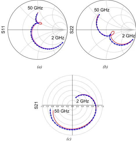
The agreement between the measured S-parameters (blue traces in Fig. 2.6) and the model (red traces in Fig 2.6) is quite good.
1 1.5 2 2.5 3 3.5 4 -0.5 -0.3 -0.1 0.1 0.3 √Ids/gm Vgs (V)
(a) (b)
(c) (d)
Fig. 2.6. Linear performance of the 4x15 µm OMMIC mHEMT transistor. Blue, measurements. Red,
simulation of the model (Fig. 5). (a) S11. (b) S22. (c) S21. (d) S12.
For the noise model, the Pospieszalski model [2.11] has been used and the two temperatures Td and Tg have been obtained. Tg is assumed to be equal to the ambient
temperature and 50 Ω noise figure measurements of the transistor have been made in order to get Td. The results of these measurements for Vd = 0.6 V and Id = 6.7 mA are
shown in Fig. 2.7, where the ripple is due to mismatching between the transistor and the source. The value obtained for Td is 3200 K, while the remaining resistors of the small
signal model are set to an ambient temperature Tg = 300 K. Note that noise figure
measurements were performed up to 40 GHz (Ka-band) due to the laboratory set-up available. Anyways, the noise model is reasonable extrapolated up to 50 GHz (Q-band).
A 2x15 µm (Fig. 2.8) OMMIC mHEMT was also measured to clarify the best size of the transistor to design the LNA. DC curves (Fig. 2.9) are similar to the 4x15 µm transistor (Fig. 2.3). The bias point for minimum noise (Fig. 2.10) is the same as for the 4x15 µm transistor, Vd = 0.6 V, Vg= -0.125 V. S1 1 100 MHz 50 GHz S2 2 100 MHz 50 GHz 100 MHz 50 GHz -4 -3 -2 -1 0 1 2 3 4 -5 5 S21 100 MHz 50 GHz -0.15 -0.10 -0.05 0.00 0.05 0.10 0.15 -0.20 0.20 S12
2.3 MMIC LNA design
Fig. 2.7. Noise performance over 50 Ω of a 4 x 15 µm OMMIC mHEMT transistor at room temperature
for Vd = 0.6 V and Id = 6.7 mA.
Fig. 2.8. Photo of a 2x15 µm OMMIC mHEMT transistor.
Fig. 2.9. IV curves for a 2x15 µm OMMIC mHEMT transistor. Vds: 0 to 1 V. Vgs: -1 to 0.3 V, in steps of
25 mV.
Fig. 2.10. The 2x15 µm OMMIC mHEMT transistor bias approximation for minimum noise (1). Vgs: -0.5
to 0.3 V in steps of 25 mV. Vds: 0 to 1 V, in steps of 50 mV. 1.5 2 2.5 3 26 28 30 32 34 36 38 40 NF (dB) Frequency (GHz) NF simulation NF measurement 0 100 200 300 400 500 600 700 800 0 0.1 0.2 0.3 0.4 0.5 0.6 0.7 0.8 0.9 1 Ids (mA /m m ) Vds (V) 1 1.5 2 2.5 3 3.5 4 -0.5 -0.3 -0.1 0.1 0.3 √Id s/ gm Vgs (V)
Noise measurements are performed for different drain current densities (mA/mm). The mean noise figure in 2x15 µm (Fig. 2.11(b)) transistor is 0.5 dB higher than the noise figure of 4x15 µm option (Fig. 2.11(a)). So the 4x15 µm is the best option attending to 50 Ω noise measurements at room temperature.
(a) (b)
Fig. 2.11. Noise performance versus frequency for different drain current densities (mA/mm). (a) 4x15 µm, (b) 2x15 µm transistor.
To check the goodness of the noise model a parameter called R (2.2) is defined following [2.11]. The foundry model (blue) is compared with the homemade model (red) in Fig. 2.12. Both the homemade extracted small signal and foundry models satisfy the condition, R<2, in (2.2), from DC to 50 GHz.
1 2
4 ∙ ∙ (2.2)
where N=Ropt·gn, Ropt is the real part of optimal noise impedance, and gn is the
noise conductance (1/Rn). Tmin is the minimum noise temperature.
Fig. 2.12. Parameter R. In blue the foundry model. In red the homemade model.
The major difference appears in noise parameters Rn and Sopt. The noise resistance
0 0.5 1 1.5 2 2.5 3 3.5 4 4.5 5 26 28 30 32 34 36 38 40 NF (dB ) Frequency (GHz) 0.6 V, 111 mA/mm 0.6 V, 137 mA/mm 0.8 V, 93 mA/mm 0.8 V, 116 mA/mm 0.8 V, 141 mA/mm 0.8 V, 168 mA/mm 1 V, 117 mA/mm 0 0.5 1 1.5 2 2.5 3 3.5 4 4.5 5 26 28 30 32 34 36 38 40 NF (dB ) Frequency (GHz) 0.6 V, 62 mA/mm 0.6 V, 75 mA/mm 0.6 V, 104 mA/mm 0.8 V, 51 mA/mm 0.8 V, 63 mA/mm 0.8 V, 76 mA/mm 0.8 V, 91 mA/mm 0.8 V, 103 mA/mm 0.8 V, 122 mA/mm 1 V, 63 mA/mm 1.5 1.6 1.7 1.8 1.9 2 2.1 2.2 0 10 20 30 40 50 R param et er Frequency (GHz) Homemade Model OMMIC foundry Model
2.3 MMIC LNA design
the Sopt (Fig. 2.13(c)) is close to 50 ohms so the homemade small signal model is easy to
match the optimum noise coefficient with 50 ohm input reflection coefficient.
The homemade model shows a realistic and higher noise figure over 50 Ω than the foundry model (Fig. 2.13(d)).
(a) (b)
(c) (d)
Fig. 2.13. Noise parameters and noise over 50 Ω of the 4x15 µm OMMIC mHEMT transistor. In red the
foundry model. In blue the homemade model. (a) NFmin. (b) Rn. (c) Sopt. (d) NF over 50 Ω.
2.3.2. LNA design
The MMIC LNA is a classic four stage design with transistors in common source configuration. All the stages have the same transistor size of 4 x 15 µm and the same bias point (Vd = 0.6 V, Id = 6.7 mA). Source feedback technique for the two first stages
has been used to get good noise performance as well as input matching and stability. J. Engberg [2.13] presented in 1974 an optimisation method for low-noise amplifiers, in which the use of series-shunt configurations match the input conjugate admittance to the optimum noise admittance. Moreover, with the use of lossless networks, it was considered that noise did not vary because feedback was not introducing noise itself. L. Besser [2.14] added one year later the noise variation versus series-shunt source feedback network. In [2.15] the exact noise figure formulation is presented taking into account both series and shunt feedback. In 1985 [2.16] the source feedback technique is
0 0.5 1 1.5 2 0 10 20 30 40 50 NF m in (d B) Frequency (GHz) Homemade Model OMMIC foundry Model
16 18 20 22 24 26 28 0 10 20 30 40 50 Rn ( Ω ) Frequency (GHz) Homemade Model OMMIC foundry Model
So
pt
50 GHz
100 MHz
Homemade Model
OMMIC foundry Model
1 1.5 2 2.5 3 0 10 20 30 40 50 NF ( d B ) Frequency (GHz) Homemade Model OMMIC foundry Model
introduced in X-band monolithic amplifier (8-12 GHz). In Fig. 2.14 the input conjugate reflection coefficient (blue) and optimum noise coefficient (red) are plotted in a Smith chart before (Fig. 2.14(a)) and after (Fig. 2.14(b)) a series source feedback is added to the transistor. Feedback joins both coefficients and move them to the centre of Smith chart improving matching.
(a) (b) Fig. 2.14. Noise optimum coefficient (red) and conjugate input reflection coefficient (blue). (a) Before
and, (b) after the source feedback is introduced in the transistor.
Since the first stage is the most important in terms of noise, the design should rely on simple microstrip lines for the input stage. Matching networks for the last two are designed to achieve flat gain keeping the noise of the amplifier as low as possible. Design and optimization processes are carried out using ADS Momentum simulator from Keysight Technologies. Bias networks are kept independent for each stage and they are made up of a combination of resistors and capacitors providing filtering networks. Fig. 2.15 shows the schematic of the LNA with the bias networks.
Fig. 2.15. Schematic of the four stage MMIC LNA (impedance and electrical length of microstrip lines are obtained at central frequency of 41 GHz).
The knowledge of the technological process is an important issue to be carefully 34 GHz 48 GHz Sopt S11* 34 GHz 48 GHz Sopt S11*
2.3 MMIC LNA design
layout of the LNA is presented. Layers go from the most external called FreeSpace to Ground (GND). The detail of each layer of the process D007IH used is described below. The most external conductive layers IN and TIN are placed between the first layer of Silicon Nitride (SiN) and the layer of Silicon Oxide (SiO). IN layer is the second interconnection metallic layer of TiPtAu with 1.25 µm of thickness. TIN layer is the first interconnection metallic layer of the same thickness and material than IN layer.
A via hole is in the Silicon Oxide layer to connect IN, TIN layer to next conductive layer (TE). Via hole is in CO layer made up of a dielectric deposition of Silicon Oxide with 800 µm of thickness.
Next layer is TE which forms the top electrode of the MIM capacitors. It is also used to protect the gates in TiAl and the gold lines in order to guarantee a high reliable connection. The thickness is 560 µm.
Below TE it is found the second layer of Silicon Nitride in which via hole is implemented in CG mask. This mask is formed by Silicon Nitride (Si3N4) and interconnects metals.
Next layer is BE. Formed by TiPtAu is a metallisation used as the bottom electrode of MIM capacitors. It is also used in 3 µm diodes. Its thickness is 650 nm.
A Benzocyclobutene (BCB) layer is deposited on a Silicon Nitride floor of 10 nm. It is used to support the gates of the transistors with a layer of low dielectric constant (2.65) and 800 nm of thickness. So the active parts are protected. Moreover, it is used in diodes and GaAs/NiCr resistors. In this layer there are defined via holes in CG mask to interconnect metals.
Finally, the resistive layer MD is implemented. It is used in NiCr resistors. It has a 30 nm of thickness and a resistivity of 40 Ω/square.
Fig. 2.16. Layers of the process D007IH from OMMIC foundry.
There are a lot of layers defined in the process D007IH but there are referred to the active component, the transistor. Since in the electromagnetic optimisation the microstrip networks are only included, the transistor layers are not defined in this text.
2.3.3. Yield
When a large amount of MMIC chips has to be manufactured it is important to have an estimation of how many chips will achieve the performance requirements. This information is a statistical data about variations in the elements that compose the circuit. For example, all the monolithic processes have tolerances in the resistivity of resistors, gap in capacitors, dimensions of microstrip lines, or the model of the transistors. Measuring own structures of the process (PCM, process control monitor) the probability distribution function that determines how is the variation of the components of the process is obtained. Yield analysis includes the simulation of the circuit many times where different parameters of the design are varied around their nominal value. The simulator registers each iteration like a pass or a fail depending the performance is achieved or not. This a Monte Carlo method of analysis which has the property of the precision is independent of the number of statistical variables and distributions.
The difference between the obtained yield and that expected depends directly on the iterations of the analysis done. If the number of iterations is small, the results probably will not be representative and the statistical error will be high. So it is necessary a big number of iterations in order to have a high confidence level and very low statistical error.
Main results obtained in the simulator after a yield analysis are: ∑
2.3 MMIC LNA design
Standard deviation ∑
1 (2.4)
Correlation coefficient ∑ ∑ ∙
1 ∙ ∙ (2.5)
The mean value and the standard deviation are typical indicators. The correlation coefficient denotes the quantitative variations of variable x with variable y (2.5). Moreover, it explains de variations of x and y with a third variable that usually is the time.
In next lines a yield analysis of the designed LNA is performed. The variables to be varied are the dimensions of the transmission lines, capacitor values, and some transistor parameters (gm, pinch-off, etc.).
2.3.3.1. Large signal model yield analysis
The yield analysis in large signal is necessary to evaluate the variations of the transistor. The analysis is divided into two parts: the first one is focused in Scattering parameters in the frequency band of interest (35-47 GHz) and second covers the frequency band 100 MHz – 80 GHz to analyse the stability of the LNA.
In this analysis the noise performance is not evaluated because the large signal model of the transistor has no information about noise parameters.
The goals of Scattering yield analysis in the 35-47 GHz frequency band are: |S21|2 > 25 dB.
|S11|2 < -10 dB. |S22|2 < -8 dB.
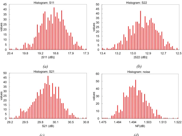
Iterations number for the analysis = 1000.
The results of the Scattering yield analysis are shown in the histograms of Fig. 2.17. These histograms represent the distribution function of the values of the Scattering parameters. The values of the mean and the standard deviation are summarized in Table 2.2.
(a) (b)
(c)
Fig. 2.17. Histograms of Scattering yield analysis in large signal model for 1000 iterations. (a) S11. (b)
S22. (c) S21.
Table 2.2. Mean and standard deviation for Scattering yield analysis of the LNA with transistor large signal model.
Parameter Mean (dB) Standard deviation (dB)
S11 -17.8 4.1
S22 -11.7 2.2
S21 27.6 8.1
The percentage of circuits that achieve the performance requirements is 60.4 %. It means, 604 chips will pass the test in a hypothetic amount of 1000 chips manufactured. This value is quite small, so an analysis in small signal will be done to compare the results.
The second analysis with the transistor large signal model is the stability. It is studied through the parameters k and µ, which they have to be greater than 1. Fig. 2.18 shows the histograms and Table 2.3 summarises the mean and deviation of these parameters. In this case the yield is the 100%, it means, all the manufactured circuits will pass the test in terms of stability.
0 20 40 60 80 100 120 32.9 27.0 21.2 15.3 9.5 3.6 values |S11 (dB)| Histogram: S11 0 20 40 60 80 100 120 17.9 14.9 12.0 9.0 6.1 3.1 values |S22 (dB)| Histogram: S22 0 50 100 150 200 0.8 7.3 13.8 20.3 26.9 33.4 values S21 (dB) Histogram: S21
2.3 MMIC LNA design
(a) (b)
Fig. 2.18. Histograms of stability yield analysis in large signal model for 1000 iterations. Parameters: (a) µ. (b) k.
Table 2.3. Mean and standard deviation for stability yield analysis of the LNA in large signal regimen.
Parameter Mean Standard deviation µ 1 1.2e-6
k 15.1 15.1
2.3.3.2. Small signal model yield analysis
In the yield analysis using the transistor small signal model, the variations are only produced in passive elements. So the transistors are excluded in this analysis. The noise performance is added to the Scattering analysis. The new goals are:
|S21|2 > 25 dB. |S11|2 < -10 dB. |S22|2 < -10 dB.
NF (noise figure) < 1.8 dB.
Iterations number for the analysis = 750.
In Fig. 2.19, the histograms for Scattering and noise are shown. In Table 2.4 mean and standard deviation simulation results are summarised. Comparing the results with the ones obtained in Table 2.3, it is clear the deviation values are now smaller and the mean values better. So the predicted yield is higher in the small signal analysis. In fact, it is a 100 % compared with 60 % in the case of large signal model. This is due to the higher influence of the active element, the transistor, in the performance of the LNA MMIC. 0 10 20 30 40 50 60 1 1 1 values μ
Histogram: μ stability parameter
0 100 200 300 400 500 600 700 11 56 101 147 192 237 values K
(a) (b)
(c) (d)
Fig. 2.19. Histograms of Scattering yield analysis in small signal model for 750 iterations. (a) S11. (b) S22.
(c) S21. (d) Noise figure.
Table 2.4. Mean and standard deviation for Scattering yield analysis of the LNA in small signal regimen.
Parameter Mean (dB) Standard deviation (dB)
S11 -18.6 0.51
S22 -12.9 0.15
S21 29.9 0.26
NF 1.49 0.007
The stability yield analysis with small signal model achieves the same results than in large signal regimen, as expected. In Fig. 2.20 the histograms for parameters k and µ are plotted, and in Table 2.5 the mean and deviation obtained are summarised.
(a) (b)
Fig. 2.20. Histograms of stability yield analysis in small signal model for 1000 iterations.
0 5 10 15 20 25 30 35 40 45 20.4 19.8 19.2 18.6 17.9 17.3 values |S11 (dB)| Histogram: S11 0 5 10 15 20 25 30 35 40 45 50 13.4 13.2 13.0 12.9 12.7 12.5 values |S22 (dB)| Histogram: S22 0 5 10 15 20 25 30 35 40 45 50 29.2 29.5 29.8 30.1 30.5 30.8 values S21 (dB) Histogram: S21 0 10 20 30 40 50 60 1.475 1.484 1.494 1.503 1.513 1.522 values NF(dB) Histogram: noise 0 5 10 15 20 25 30 35 40 45 50 1.0 1.0 1.0 1.0 1.0 1.0 values μ
Histogram: μ stability parameter
0 10 20 30 40 50 60 8.8 9.1 9.4 9.6 9.9 10.2 values K
2.3 MMIC LNA design
Table 2.5. Mean and standard deviation for stability yield analysis of the LNA with transistor small signal model.
Parameter Mean Standard deviation µ 1 1.2e-6
k 9.3 0.19
Looking forward at the yield analyses, both large and small signal models, the importance of the active element, the transistor, is significant because the variation of its parameters dominates the global performance of the LNA. The critical performance parameter is the gain due to variations of pinch-off voltage and transconductance gm of the transistor.
One of the most important issues in an amplifier is the stability. It has been verified that the LNA is stable under any variation of its components and for both transistor models, small and large signal.
2.3.4. Connection of the LNA: Bonding wire
When the MMIC LNA is integrated in a chassis it is very important its connection with the access lines, both bias and radio frequency (RF). The usual way to do that interconnections, in high frequency designs, is bonding gold wires to MMIC access pads.
In Fig. 2.21 the simulation of the MMIC gain and noise performance is shown for different bonding wire lengths to RF pads, from 0 to 600 µm. The gain decreases as the bonding wire is longer. Meanwhile the noise increases. This effect is more significant in high frequencies due to the inductive behaviour of the wire.
So the connection bonding wires should be shorter than 300 µm in order to not degrade gain and noise performances.
Fig. 2.21. Gain and noise simulation of the MMIC LNA for different bonding wire lengths, from 0 to 600 µm stepped by 150 µm. 0 10 20 30 40 50 60 0 2 4 6 8 10 12 30 35 40 45 50 S2 1 (d B) NF (d B) Frequency (GHz) NF sim. NF wire 150 um NF wire 300 um NF wire 450 um NF wire 600 um S21 sim. S21 wire 150 um S21 wire 300 um S21 wire 450 um S21 wire 600 um
2.3.5. Manufacturing
Once all the optimisation stages are finished and the design is validated, the layout is sent to the foundry to be manufactured. The adjusted size 3 x 1 mm2 for the LNA is a standard used in OMMIC foundry. A picture of the manufactured MMIC LNA is shown in Fig. 2.22.
Fig. 2.22. Photograph of the manufactured MMIC LNA (size 3 x 1 mm2).
2.4. LNA measurements and characterisation
2.4.1. Measurements on wafer at room temperature
Firstly the LNA is characterised on wafer at room temperature. These measurements are made in a coplanar probe station from Cascade Microtech (Fig. 2.23). RF characterisation is performed using a Keysight E8364A network analyser. Noise measurements (Fig. 2.24) are performed using the Y-factor method with a Keysight N8975A noise figure analyser. An external down-converter is used to measure in the 33-50 GHz frequency band because the noise figure analyser only has the capability to measure up to 26.5 GHz. A 6 dB attenuator at the output of the noise source (346C_K01 from Keysight) is used to reduce the excess noise ratio (ENR) in order to improve the noise measurement accuracy [2.17].
2.4 LNA measurements and characterisation
Fig. 2.24. MMIC in the coplanar probe station for noise measurement.
Fig. 2.25(a) shows the linear performance (S-parameters) result, while noise temperature and insertion gain are shown in Fig. 2.25(b). The average gain in the 33-50 GHz frequency band is 28.2 dB. Input return loss is better than 4 dB and output return loss is better than 11 dB within the whole band. The average noise temperature is 145 K in the 33-50 GHz frequency band, and the minimum noise temperature is 101 K near 45 GHz. The gain achieved is quite lower than 30 dB expected (red traces in Fig. 2.25(b)) because the transistors used in the model during the design stage had a higher transconductance compared with the ones used in the manufactured MMIC. Moreover, the measured noise temperature response is quite flat and lower at high frequencies than the simulation approach.
The bias point for getting the lowest noise in the amplifier at room temperature is
Vd = 0.61 V and a total current Id = 24.9 mA for the 4 stages, with a DC power
consumption of 15.2 mW. These values are very close to the bias point for lowest noise provided by (2.1), validating this expression for the initial design.
(a) (b)
Fig. 2.25. On wafer MMIC LNA measurements at room temperature, Vd = 0.61 V and Id = 24.9 mA.
(a) Scattering parameters. (b) Noise temperature.
-40 -30 -20 -10 0 10 20 30 40 20 25 30 35 40 45 50 S ( dB) Frequency (GHz) S21 S11 S22 0 5 10 15 20 25 30 35 40 0 100 200 300 400 500 600 700 800 30 35 40 45 50 Gi (d B ) Tn ( K ) Frequency (GHz) Tn Tn_sim Gi S21_sim
2.4.2. Amplifier characterisation at cryogenic temperature
For the characterisation of the MMIC LNA at cryogenic temperatures a suitable module has been machined. This module is made of aluminium in order to improve the thermal conductivity and to reduce the total weight. Afterwards, the chassis is nickel and gold plated.
The chassis has two cavities: one for the chip and the high frequency access lines with 1.2 mm width, whereas the other houses the biasing networks as shown in Fig. 2.26. DC bias accesses are narrow channels in order to avoid resonances in the cavity. The chassis is equipped with 1.85 mm coaxial connectors, and the transition between these connectors and the microstrip lines is made using sliding contacts to allow flexibility in the joints during cryogenic operation. The off-chip bias networks are made up of capacitors, resistors and protection diodes to prevent potential low-frequency instabilities.
Fig. 2.26. Detail of the MMIC LNA assembly inside the chassis.
At cryogenic temperature the noise measurement was performed using the cold-attenuator technique [2.18] with a 20 dB attenuator module [2.19] inside the cryostat. The noise source is connected directly to the cryostat input line. In Fig. 2.27 the MMIC LNA chassis is presented clamped to the cold base inside the cryostat, just before a cooling cycle.
2.4 LNA measurements and characterisation
Fig. 2.27. Photo of the MMIC LNA inside the cryostat.
Three units, shown in Fig. 2.28, have been assembled with similar results in terms of noise and gain at cryogenic temperature. Each chassis has a different wire bonding length soldered to the MMIC. Moreover, in the last unit assembled (chassis #03) the MMIC was placed on a Molybdenum pedestal, instead directly on the chassis (on Aluminium). The coefficient of thermal expansion (CTE) of Molybdenum is similar to the Gallium Arsenide substrate of the MMIC (see Table 2.6). This way it is assured the MMIC does not suffer mechanical stress during a cooling cycle.
Table 2.6. Coefficient of thermal expansion (CTE) for different materials used in LNA assemblies.
Material CTE (ppm/K) @ 20ºC Molybdenum 4.8
GaAs 5.8 Aluminium 23.1
Fig. 2.28. Three chassis with the MMIC LNA assembled.
Fig. 2.29 shows the measured temperature and associated gain for the three LNA modules at a physical temperature of 15 K. The best results were obtained for unit #03 with 300 µm wire bonding lengths (green trace in Fig. 2.29) and this amplifier achieves an average gain of 27.3 dB and an average noise temperature of 18.4 K in the whole
33-50 GHz frequency band, with a minimum of 13.5 K at 45 GHz. The DC power consumption is only 4.1 mW, Vd = 0.37 V and Id = 11.2 mA.
The decrease of gain and increase of noise at 47 GHz seems to be due to the bonding wires and microstrip to coaxial transition effects, since it has not been observed in on wafer measurements. These effects could be minimized using rectangular waveguide to microstrip transitions, because better return loss could be achieved.
Fig. 2.29. Measured insertion gain and noise temperature for the three assembled LNA modules at
physical temperature of 15 K, Vd = 0.37 V and Id = 11.2 mA.
2.4.3. Comparing the LNA performance with other published works
The figure of merit (FOM) in (2.6), defined in [2.6], has been used in order to evaluate the performance of the LNA for radio astronomy receivers. This FOM includes linear gain (G), bandwidth (BW (GHz)), noise factor (F), and DC power consumption (PDC (mW)). The results of the MMIC LNA are compared in Table 2.7 with other published works. The noise achieved at cryogenics is close to the one obtained in InP process [2.4] in a similar frequency band. The FOM value at cryogenics is the highest mainly because the very low DC power (4.1 mW, Vd = 0.37 V and Id = 11.2 mA).
Moreover, the FOM obtained at room temperature is also the highest due to the good noise performance of the presented MMIC LNA.
∙ 1 ∙ (2.6) 0 6 12 18 24 30 36 0 15 30 45 60 75 90 33 34 35 36 37 38 39 40 41 42 43 44 45 46 47 48 49 50 Gi ( dB) Tn (K ) Frequency (GHz) Chassis #1, Tn Chassis #2, Tn Chassis #3, Tn Chassis #1, Gi Chassis #2, Gi Chassis #3, Gi
2.4 LNA measurements and characterisation
Table 2.7. Comparison of previously reported LNA and this work.
Reference BW (GHz) G (dB) NF (dB) Tn (K) PDC (mW) FOM Process [2.4] 24-40 28 0.19 13.2 * 10.8 832 130 nm InP HEMT [2.5] 27.3-50.7 23.1 3.7 390 ** 88 2.8 150 nm GaAs mHEMT 30-50 19.5 0.62 44.8 * 21.4 57.5 [2.6] 27-45 25 3.1 302 ** 9 34 100 nm GaAs pHEMT [2.7] 30-50 19.8 3.4 345 ** 46 3.6 150 nm GaAs mHEMT 23 0.34 23.4 * 10 347 [2.8] 37-53.2 32.5 3.2 316 ** 152 4.1 150 nm mHEMT 32-50 29.5 2.8 263 ** 140 4.2
This work 33-50 28.2 1.8 145 ** 15.2 55.6 70 nm GaAS mHEMT 27.3 0.27 18.4 * 4.1 1504
(*) module. (**) on wafer.
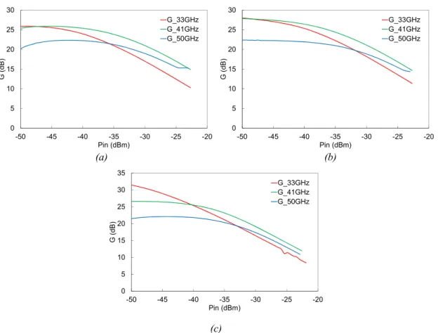
2.4.4. Gain compression: P1dB
The gain compression concludes the LNA characterisation. This measurement is realised at room temperature with the set-up shown in Fig. 2.30. A signal generator (reference 83650B from Hewlett Packard) is used at the input of the LNA to sweep the input power from -50 to -20 dBm, stepped by 0.5 dB. The output power is measured with a power meter (reference E4418B from Hewlett Packard) and a power sensor (also from Hewlett Packard, reference 8487A) which allows to measure a power range from -30 to 20 dBm. The bias point for each LNA module is set to Vd = 0.68V,
Id1 = 6.7 mA, and Id234 = 6.4 mA.
Fig. 2.30. P1dB set-up for the three assembled LNA modules at room temperature.
The measured results for each chassis are plotted in Fig. 2.31 at three representative frequencies, the central point at 41 GHz, and the ends of the band at 33 and 50 GHz. The 1-dB gain compression points referred at the output of the LNA are listed in Table 2.8. The gain compression performance is improved along the frequency
band because the maximum P1dB value is obtained at the highest frequency, 50 GHz, where the gain is lower. Best point of -10 dBm output power is achieved in chassis #01.
(a) (b)
(c)
Fig. 2.31. Gain compression, P1dB, for the three assembled LNA modules at room temperature. Chassis
(a) #01, (b) #02, (c) #03.
Table 2.8. P1dB value (output power) for the three assembled LNA modules at room temperature.
Chassis 33 GHz 41 GHz 50 GHz #01 -17.7 -12.9 -10.1 #02 -18.8 -15.2 -15.6 #03 -16.4 -13.5 -15.5
2.5. Impact of the LNA in a radiometer
The impact of the cryogenic performance of the MMIC LNA is analysed into a radio astronomy receiver, a radiometer. Considering the scheme of Fig. 2.32, the total receiver equivalent noise temperature (T'rec) can be calculated through (2.7)-(2.10). The
contributions of temperature come from the feed system, Lfeed in (2.8), the back-end
module (BEM), TBEM in (2.7) and the LNA, TLNA and GLNA in (2.7).
∙ 1 ∙ (2.7) 1 ∙ ∙ (2.8) 0 5 10 15 20 25 30 -50 -45 -40 -35 -30 -25 -20 G (d B) Pin (dBm) G_33GHz G_41GHz G_50GHz 0 5 10 15 20 25 30 -50 -45 -40 -35 -30 -25 -20 G (d B) Pin (dBm) G_33GHz G_41GHz G_50GHz 0 5 10 15 20 25 30 35 -50 -45 -40 -35 -30 -25 -20 G (dB ) Pin (dBm) G_33GHz G_41GHz G_50GHz
2.6 Conclusions
Fig. 2.32. Basic scheme of a radio astronomy receiver.
The system noise temperature including the antenna and the receiver is defined in (2.9). Finally the operation noise temperature of the radiometer includes the sky temperature (2.10).
(2.9) (2.10) Taking a BEM noise temperature of 400 K, feed system losses of 0.5 dB (at a physical temperature, Tp, of 15 K), and connection cable losses of 7 dB, the receiver temperature (T'rec) is 29 K. Looking at (2.7), the principal noise contribution comes
from the LNA (18 K). The gain of the LNA is not high (27 dB) and the contribution of cables and BEM is considerable (11 K).
Adding to the receiver the contribution of the antenna (6.8 K) the system noise temperature (2.9) of the radiometer is 36 K. And the total operation noise temperature (2.10) taking into account the sky is 51 K.
The LNA minimizes the noise contribution of the back-end but there will be an important contribution in the total noise coming from the components in front of the LNA. Every kelvin improvement in the LNA will reduce in the same quantity the operation temperature of the receiver.
2.6. Conclusions
The design and characterisation of a broadband monolithic cryogenic low-noise amplifier developed for radio astronomy applications in the 33-50 GHz frequency band have been presented in this chapter. The LNA is a four-stage common-source configuration manufactured on 70 nm GaAs metamorphic technology from OMMIC foundry.
The amplifier exhibits a gain of 28 dB and a noise temperature of 145 K in the 33-50 GHz frequency band for on wafer measurements at room temperature. When the
amplifier is cooled down to 15 K, the gain is 27.3 dB and the average noise temperature is 18.4 K. The DC power consumption at cryogenics temperatures is only 4.1 mW.
The impact of the LNA performance in the operation noise temperature of a radiometer has been analysed remarking the importance of the LNA as the element who mainly fixes the noise and minimizes the contributions of back-end module in the receiver.
2.7. References
[2.1] Chau-Ching Chiong, Wei-Je Tzeng, Yuh-Jing Hwang, Wei-Ting Wong, Huei Wang, and Ming-Tang Chen “Design and Measurements of Cryogenic MHEMT IF Low Noise Amplifier for Radio Astronomical Receivers,” Proceedings of the 4th European Microwave Integrated Circuits Conference, September 2009, pp. 1-4.
[2.2] Christophe Risacher, Erik Sundin, Victor Perez Robles, Miroslav Pantaleev, and Victor Belitsky, “Low Noise and Low Power Consumption Cryogenic Amplifiers for Onsala and Apex Telescopes,” 12th GAAS Symposium, Amsterdam 2004.
[2.3] P. Kangaslahti, T. Gaier, M. Seiffert, S. Weinreb, D. Harding, D. Dawnson, M. Soria, C. Lawrence, B. Hooberman, A. Miller, “Planar Polarimetry Receivers for Large Imaging Array at Q-band,” in IEEE 41st European Microwave Conference, October
2011, pp. 934-937.
[2.4] Joel Schleeh, Niklas Wadefalk, Per-Ake Nilsson, J. Piotr Starski, and Jan Grahn, “Cryogenic Broadband Ultra-Low-Noise MMIC LNAs for Radio Astronomy
Applications,” IEEE Transactions on Microwave Theory and Techniques, 2013, vol. 61, no. 2, pp 871-877.
[2.5] Shou-Hsien Weng, Wei-Chu Wang, Hong-Yeh Chang, Chau-Ching Chiong, and Ming-Tang Chen “A Cryogenic 30-50 GHz Balanced Low Noise Amplifiers Using a 0.15-µm MHEMT Process for Radio Astronomy Applications,” IEEE International
Symposium on Radio-Frequency Integration Technology (RFIT), 2012, pp. 177-179.
[2.6] Shou-Hsien Weng, Wei-Chu Wang, Hong-Yeh Chang, Chau-Ching Chiong, and Ming-Tang Chen “An Ultra Low-power Q-band LNA with 50% Bandwitdth in WIN GaAs 0.1-µm pHEMT Process,” Asia-Pacific Microwave Conference Proceedings, 2013, pp. 713-715.