Advanced Computational Design of Intermediate-Band Photovoltaic Material V-substituted MgIn2S4.
I. Aguilera, P. Palacios, K. Sánchez, P. Wahnón
Instituto de Energía Solar & Dept. Tecnologías Especiales, Universidad Politécnica de Madrid, Ciudad Universitaria s/n, Madrid, 28040, Spain.
ABSTRACT
An intermediate-band material based on thiospinel semiconductor MgIn2S4 is presented.
This material is proposed as high efficiency photovoltaic material for intermediate-band solar cells. We analyze V substitution for In in the parent compound MgIn2S4 and the formation of the
V d-states intermediate band. For the proper characterization of the width and position of this band inside the band gap, the standard one-shot GW method within the plasmon-pole
approximation is applied. The electronic properties thus obtained are discussed and compared to those studied with Density Functional Theory (DFT), and the advantages and the limitations of the two methods are discussed. In addition, DFT electronic-charge density analysis is shown.
INTRODUCTION
Thin-film technology for solar cells is emerging as one of the most promising proposals for higher-efficiency, lower-cost photovoltaic solar cells. The combination of the thin-film technology with the intermediate-band (IB) concept [1] could be the answer to the present efficiency-cost compromise.
A partially-filled narrow band isolated from the valence and conduction bands of a host semiconductor would allow the absorption of sub-band-gap energy photons. For a solar cell, this would result, in the creation of additional electron-hole pairs and, in principle, in an increase in photocurrent without a decrease in open-circuit voltage. A cell based on such an approach could reach theoretical efficiencies up to 63.2% [1].
In this context, the first materials proposed were derivatives of chalcopyrites. Studies of intermediate-band materials based on CuGaS2 have already been presented [2-4], showing a
potential suitability for enhanced photovoltaic applications. In these materials, Ga atoms were replaced by Ti or Cr at tetrahedral sites.
For the thiospinel family of compounds, such as the one studied in this work, the group-III atoms (In) occupy octahedral sites. The transition metal will thus be octahedrally coordinated in contrast with the case of chalcopyrite-based compounds. This situation for the transition metal is, in principle, more stable.
The compound MgIn2S4 was chosen as host semiconductor because its band gap ranges
from 2.1 to 2.28 eV [5,6], which are close to the optimum gaps for the implementation of an IB
material. The structure of MgIn2S4 is a cubic spinel structure, where sulfurs form a FCC lattice
with Mg occupying tetrahedral sites and In octahedral sites. Substitution of V for In atoms at tetrahedral sites allows the formation of an IB with the desired characteristics [7].
THEORY
Ground-state density functional theory (DFT) [8] calculations were performed with the plane-wave codes ABINIT (AB-INITio) [9] and VASP (Vienna Ab-initio Simulation Package) [10], in the local-density approximation (LDA). Full relaxations of ion positions and lattice structure were carried out within this approach, for both the parent semiconductor and the V-substituted material.
For the band structure calculations, pseudopotentials using the Troullier-Martins scheme [11], were constructed with the code fhi98PP [12] to describe electron-ion interactions. The package fhi98PP is a code meant for the generation of norm-conserving pseudopotentials. It also allowed us to check the transferability of our pseudopotentials, and to detect ghost states in order to avoid them. Semicore states were included explicitly as valence states for In, V and Mg, in order to account for the spatial superposition of the outermost valence and the semicore.
To accurately predict the band gap of the pure semiconductor and the position of the intermediate band inside this gap, GW (with G, the one-particle Green’s function and W, the screened Coulomb potential) [13,14] calculations were performed. The plasmon-pole
approximation was used. The DFT ground-state was used as a starting point for the one-shot GW calculation. In this approach, LDA eigenvalues and eigenfunctions are used to construct G and W instead of a self-consistent treatment. This is usually called G0W0.
DISCUSSION
MgIn2S4 pure semiconductor:
For the pure semiconductor, ground-state calculations with LDA led to a band gap value of 1.59 eV. As the value of the band gap of semiconductors is known to be underestimated in DFT calculations, the GW approach was considered to overcome this problem. It is crucial for the determination of the formation of a potential intermediate band, to start from a
semiconductor with an accurately predicted band gap. G0W0 applied to this compound produces
a band structure practically equal to that of LDA, but with a rigid shift applied to the conduction states. In other words, the dispersions of the bands are retained with respect to the LDA but the band gap is increased up to 2.87 eV.
MgIn2S4 has an experimental band gap of 2.28 eV at low temperature [6]. It is known
[15] that in nature, this material presents a degree of inversion, i. e., some cations interchange their positions in the cell structure and thus, some Mg atoms occupy octahedral sites and some In atoms tetrahedral sites. The discrepancy between the G0W0 value of the band gap and the
Apart from the improvement in the band gap, the second main effect of the GW calculation is the effect on the position of the In d states. In the LDA bands, these are situated 13.5 eV below the top of the valence band. With the application of G0W0 we obtain a position for
these d-states of 15 eV below the top valence.
Once the parent semiconductor is well characterized, we proceed to the substitution of V for an In atom.
Mg2VIn3S8 intermediate-band material:
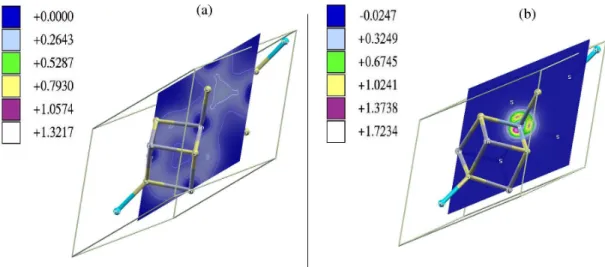
Electronic-charge density of the pure and the doped compounds are compared in figure 1. Left panel represents a cut of the density of the pure semiconductor in the (1 0 0) plane of the primitive cell. Figure 1(b) shows the difference between the spin-up and down electronic density after the substitution with vanadium. As can be seen, the spin polarization appears around the inserted transition metal. The charge induced by the metal is clearly seen from the comparison between the two images. This charge density around the metal is responsible for the formation of the narrow intermediate band (see figure 2).
Figure 1. Electronic-charge density of (a) MgIn2S4 and (b) difference between up and
spin-down density for the V-substituted alloy.
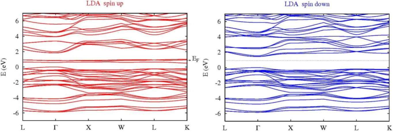
DFT ground-state band diagrams of V-substituted MgIn2S4 are shown in figure 2. The
structure of a semiconductor is retained for spin-down states, but in the spin-up band diagram the
t2g states of the vanadium form an intermediate band inside the band gap of the host
semiconductor, whereas the eg states hybridize with the conduction band (CB). The new transition-metal band shows the desired characteristics for an efficient intermediate-band
Figure 2. Spin-up and down band diagrams of Mg2VIn3S8 intermediate-band compound,
calculated within the DFT-LDA approximation. The top of the valence band is adjusted to zero.
Figure 3 shows the result of the G0W0 calculation. The band gaps from the valence band
to the conduction band is opened to reach 2.66 eV for spin up, and 2.25 eV for spin down. These values are lower than the theoretical band gap of the pure semiconductor. This is explained because the empty d-states which hybridize with the conduction band make the bottom CB to be placed lower than the original CB of the host semiconductor.
Figure 3. Spin-up and down band diagrams of Mg2VIn3S8 intermediate-band compound,
calculated within the G0W0 approximation. The top of the valence band is adjusted to zero.
The new intermediate band is predicted to be placed 0.69 eV below the CB, which is very close to the ideal situation [1]. Additionally, it lies around 1.59 eV over the top of the valence band, and has a width of around 0.38 eV.
CONCLUSIONS
obtained applying a one-shot GW on top of the LDA ground-state. An intermediate band with the features needed for photovoltaic applications is predicted.
However, it is known [17,18] that usually for materials with d electrons, it is important to use a better starting point than DFT. For this reason, restricted self-consistent static GW
calculations within the Coulomb Hole and Screened Exchange approximation (COHSEX) [13,19] are under way to be used as a better starting point instead of LDA. COHSEX approach lies in a static approximation to the W in the GW method. Self-consistent COHSEX
wavefunctions have been demonstrated [20] to be closer to the quasiparticle wavefunctions than the DFT ones. A G0W0 calculation made on top of COHSEX could be, in principle, more
accurate. The exact degree of accuracy remains to be studied; as such calculations have never been reported before for an intermediate-band material. This study will allow us to evaluate the reliability of the GW methods for the prediction of electronic structure of intermediate-band materials.
ACKNOWLEDGMENTS
This work was supported by the Consolider Ingenio 2010 Program, through the projects GENESIS-FV (ref. CSD2006-04) and the FOTOMAT project (MAT2009-14625-C03-01) of The Spanish Ministry of Education and Science. I.A. would also like to thank the MEC for a FPU grant and K.S. acknowledges a grant from Com. de Madrid and European Social Fund.
REFERENCES
1. A. Luque and A. Martí, Phys. Rev. Lett. 78, 5014 (1997).
2. P. Palacios, K. Sánchez, J. C. Conesa, and P. Wahnón, Phys. Status Solidi A 203, 1395 (2006).
3. P. Palacios, K. Sánchez, J. C. Conesa, J. J. Fernández, and P. Wahnón, Thin Solid Films 515, 6280 (2007).
4. P. Palacios, K. Sánchez, P. Wahnón, and J. C. Conesa, J. Solar Energy Eng. 129, 314 (2007).
5. P. M. Sirimanne, N. Sonoyama, and T. Sakata, J. Solid State Chem. 154, 476 (2000). 6. M. Wakaki, O. Shintani, T. Ogawa, and T. Arai, Jpn. J. Appl. Phys. 19, 255 (1980). 7. P. Palacios, I. Aguilera, K. Sánchez, J. C. Conesa, and P.Wahnón, Phys. Rev. Lett. 101,
046403 (2008).
8. P. Hohenberg, W. Kohn, Phys. Rev. B 136, 864 (1964); W. Kohn, L. J. Sham, Phys. Rev. A
140, 1133 (1965).
9. X. Gonze et al., Z. Kristallogr. 220, 558-562 (2005).
10. G. Kresse and J. Hafner, Phys. Rev. B 47, RC558 (1993); G. Kresse and J. Furthmüller,
Phys. Rev. B 54, 11169 (1996).
11. N. Troullier, and J. L. Martins, Phys. Rev. B 43, 1993 (1990).
12. M. Fuchs, and M. Scheffler, Comput. Phys. Commun., 119, 67-98 (1999). 13. L. Hedin, Phys. Rev. 139, A796 - A823 (1965).
17. F. Aryasetiawan and O. Gunnarsson Phys. Rev. Lett. 74, 3221 - 3224 (1995).
18. S. V. Faleev, M. van Schilfgaarde, and T. Kotani, Phys. Rev. Lett. 93, 126406 (2004). 19. F. Bruneval, N. Vast, L. Reining, Phys. Rev. B 74, 045102 (2006).