Wake up Radio Architecture for Wireless Sensor
Networks Using an Ultra Low Power FPGA
Blank for blind revision
line 1 (of Affiliation): dept. name of organization line 2: name of organization, acronyms acceptable
line 3: City, Country line 4: e-mail address if desired
Blank for blind revision
line 1 (of Affiliation): dept. name of organization line 2: name of organization, acronyms acceptable
line 3: City, Country line 4: e-mail address if desired
Abstract—In this paper an implementation of a Wake up Radio (WuR) with addressing capabilities based on an ultra low power FPGA for ultra low energy Wireless Sensor Networks (WSNs) is proposed. The main goal is to evaluate the utilization of very low power configurable devices to take advantage of their speed, flexibility and low power consumption instead of the traditional approaches based on ASICs or microcontrollers, for communication frame decoding and communication data control.
Keywords-Wireless Sensor Networs;Wake up radio; low power FPGA; energy efficiency; addressing capabilities; On-demand communicaitons.
I. INTRODUCTION
The number of applications for wireless sensor networks is growing continuously. The most extended applications are based on ultra low energy WSNs [1]. Main characteristics of this WSN are the low duty cycle of the applications (~1%) and low data rates (< 1 bit per second).
In order to maximize the lifetime of the nodes for this kind of applications, it is necessary to improve the energy efficiency of the system. The most power hungry element of a node is usually the communication stage. Furthermore, most of the power can be wasted listening to the communication channel unnecessarily, waiting for remote data. For this reason a lot of work has been done in order to improve the efficiency of communications, data dissemination, synchronization, etc. [2]
A lot of research work is focused on more efficient communication protocols, mainly by improving the usage of the communication channel. For WSNs applications, this is done by means of the medium access control (MAC) protocol. The most important MAC protocols for WSN can be divided into two main groups, Time Domain Medium Access (TDMA) and Contention-based Medium Access protocols.
The TDMA protocols, LMAC [3], TRAMA [4], PEDAMACS [5], etc., divide the channel available time into slots and only allow nodes to send messages in their own slot. These kind of protocols are theoretically the most energy efficient because the nodes turn on the radio only during their slots and solve problems regarding to interferences among nodes. But it also presents important drawbacks, the main one is the scalability, because if the topology of the network changes (new nodes are introduced, or some nodes are
unreachable) it is necessary to change the slots assignment. Making a trustable slot assignment policy needs a very accurate synchronization among the nodes. Therefore, TDMA protocols are hard to use in real WSNs deployments.
Contention-based MAC protocols (S-MAC [7], T-MAC [8], B-MAC [6], among others) carry out the medium access control by performing carrier sense in the senders combined with periodical listen/sleep scheme in the receivers. This group of protocols is the most spreaded in WSNs. This group of protocols is quite robust and permits dynamic topology of the WSN. With properly duty-cycle policies it is possible to achieve good results for energy savings, but in ultra low duty-cycle applications a tradeoff between latency and energy wasting should be accomplished. In these cases, the two main drawbacks are the need of long preambles and the high latency for multi hop data communication.
In order to overcome the synchronization problems of the TDMA and to avoid the periodic listening of the Contention-based MAC protocols on-Demand schemes can be used. These schemes are not only used in communications, but also, in sensing, acting or any tasks that should be accomplished by a node. The basic idea of these schemes is that the on-demand element should be active only if it has been demanded externally, i.e., by a parent node. In the communication control, this means that the main radio channel is switched on only if an event that requires communications occurs, i.e., a neighbor node wants to communicate with the demanded node; otherwise the radio remains switched off. Usually, an ultra low power auxiliary radio channel is used to wake up a distant node. This auxiliary radio, known as Wake up Radio (WuR), is used for non-intense data communications; only simple data, like the address or a short command, is included. This kind of communications are completely asynchronous and unslotted, avoiding the synchronization problem of the TDMA based protocol and the periodic listening of contention based schemes.
estimation with different architectures in the literature are given in Section VI.
II. WAKE UP RADIOS
Wake up Radios are the basic circuits for the on-demand communications scheme. The WuR handles the sending and receiving of wake up messages that switch on the main processing unit or the main radio of the required node.
The basic requirements for wake up radio based wireless sensor networks are proposed in [9]:
• Low power consumption should be a low percentage of the power consumption of the node in standby without WuR.
• High sensitivity. A node should not loose wakeup calls.
• Resistance to interference. False wakeups should be avoided.
• Fast wake-up. The latency of the network should be at least the same as the periodic listening schemes based networks.
Low power consumption is mandatory for the WuR receiver. Indeed, there are wake up schemes that use a single receiver and share the main radio front end for high data traffic operation and for the wake up functionality. The power consumption of the WuR receivers ideally is ‘0 W’, all the necessary energy is harvested from the Wake up message. But this is quite complicated in real applications for WSNs: in order to get a fast response, a lot of power might be emitted by the node, otherwise whether the WuR response is too slow, or the nodes have to be close to each other (a few centimeters). This makes WuR harvester hard to use in real application.
Since the ‘0 W’ power receiver is not suitable for real WSNs applications, ultra low power receivers should be used. The power consumption has to be an order of magnitude below the power consumption of the node without the WuR.
Achieving an ultra low power receiver implies the use of a simple modulation scheme that simplifies the demodulation on the receiver side. This usually impacts on the throughput of the WuR channels; however, the size of the wake up message should not be greater than a few bytes and a high throughput is not necessary.
Regarding sensitivity and resistance to interference a tradeoff between hardware complexity and quality of the communications must be set. For better performance, bigger antennas, more complex modulation and demodulation schemes, and higher power consumption should be considered. The modulation has to be simple in order to get an easy demodulation, the most typical modulation used by WuR based systems are: OOK (On Off Keying) or 2ASK (2 levels Amplitude Shift Keying) [10]; assuming that the antenna is on the size of the node, the minimum accepted sensitivity will be set by the maximum distance reachable without losing wake up calls. Usually 5 meters is the minimum accepted distance. In order to avoid false wake ups, addressing techniques can be used on the wake up message.
Obtaining the fastest wake up depends not only on the emitter but also on the processing speed of the message. This depends on the complexity of the message, the hardware availability and the performance of the algorithm that decodes the wake up messages. Message decoding is faster if dedicated hardware is available than if the message is decoded in the main processing unit, which should be awaken before decoding the data. The use of microcontrollers introduces a non-negligible latency in the process because of wake up time and increases the power consumption, because the time employed by the microcontrollers in the decoding task must be taken into account.
A. Related Work
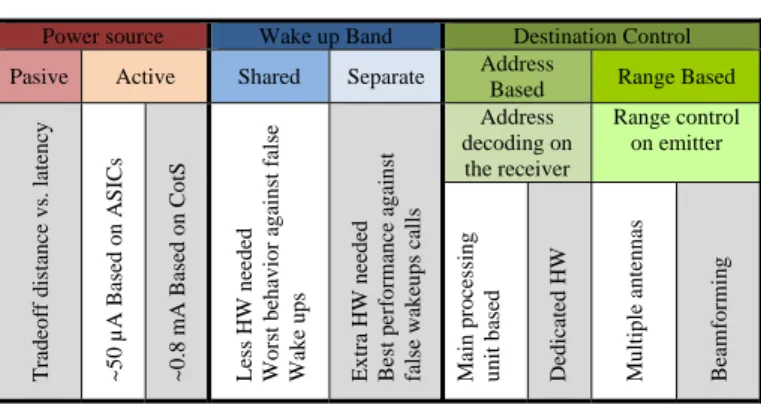
During the last years different works in the literature are focused on the implementation of wake up techniques for wireless sensor networks The design of ultra low power receivers based on integrated circuits, passive receivers, efficient communication protocols and even wake up circuits based on acoustic or infrared signals are some examples of the active topics on this field. In [11] examples of different solutions and works can be found and TABLE I. summarizes the classification done by the authors.
TABLE I. WAKE UP RADIO CHARACTERISTICS
The work presented in this paper is focused on a complete radio system for the wake up channel, with the aim of avoiding false wake ups caused by sharing the channel with the data communications radio which is one of the main problems of the systems with only one receiver. Since the goal is to implement a real WuR system, the works based on designing ASICs are out of the main focus of the present work, while the works based on components of the shelf (CotS) are deeply analyzed.
This work is focused on active receivers, with dedicated channel and addressing capabilities with dedicated hardware. The related work is presented below.
In [12], Langedoen et al. propose a wake up radio for the BT-Node platform, working at 868 MHz. Its main characteristics are: shared channel between WuR and main radio; addressing capabilities based on dedicated hardware and a low power microcontroller (PIC12F683). A BT-Node [13] is used including a CotS based receiver. In this implementation the PIC is used to perform A/D conversion in order to discriminate between ‘0’ and ‘1’ and message decoding. A WuR prototype working at a distance of 2 meters with high resistance to interferences, but with very high power consumption, mainly
Power source Wake up Band Destination Control
Pasive Active Shared Separate Address
Based Range Based
T rad eof f di sta n ce v s. late nc y ~50 µA B as ed o n A S IC s ~0. 8 m A B ase d on C o tS L ess H W ne ed ed Wors t be ha vi or a g ai nst f als e
Wake ups Ex
tr
a HW ne
due to the PIC used to decode the wake up messages signal is achieved.
In [14], Ansari et al. present a circuit board that can be used as an external peripheral for the Telos-B [15] platform. The solution implemented uses a separate channel for the WuR with addressing capabilities using the main processing unit of the node. The WuR is based on a Texas instruments low power radio and a RF amplifier in the emitter side. For the implementation of the receiver a three-stage low power consumption based on a CotS receiver is designed. The first stage is an ad-hoc antenna and a matching network. The second stage is a voltage multiplier to amplify the signal that also acts as envelope detector. Finally, a digital comparator to get the digital values of the RF signal and as over-voltage protection is used. The main drawback of this proposal is the use of the microcontroller unit in the address decoding process. This introduces extra latency and extra power consumption, due to the time needed to wake up the microcontroller and the execution of the task. Since no other identification mechanism is included in their solution, the microcontroller needs to wake up every time a wake up call arrives to the node, even if the node is not the desired destination.
In TABLE III. the main characteristics of these platforms as well as other solutions are shown.
After analyzing the work in the literature, a new architecture for WuR is proposed in this paper. In this WuR, dedicated hardware with ultra low power FPGAs is proposed in order to overcome the problems presented in the aforementioned works. The FPGA will contain the hardware involved in message decoding, and resources control capabilities. This allows accomplishing the task in a faster time and more energy efficient way than in the traditional microcontrollers used in WSN.
The main characteristics of ultra low power FPGAs are the capability to switch on in a very fast time (1 µs versus 6 µs of a regular Texas Instruments MSP430), and being able to remain in sleep state without losing their configuration with ultra low power consumption (few µW).
III. IMPLEMENTING WAKE UP RADIO TRANSCEIVERS As it has been presented before, the hardware of the WuR device should be designed and chosen carefully, in order to achieve the requirements about power consumption, range and sensitivity.
Three different ways to get a functional WuR transceiver can be followed:
1) Using a full external transceiver in order to make the modulation/demodulation process and filtering. This can be done in two ways
a) With a specific design based on discrete components, optimizing the design in power consumption. There are some examples in the state of the art, but the results are mainly based on simulation and unavailable in the market.
b) Using a commercial transceiver, looking for the best option in the market. Nowadays, most of the low power transceivers are designed to work connected
directly to a microcontroller, based on standard buses, mainly SPI. This is an inconvenience when work with an FPGA; in order to get better processing speed a direct connection can be better. Some products are available in the market with direct interconnection interface but with a power consumption of ~ 2 mA in reception, one order of magnitude over the target.
2) Using a commercial emitter and a full custom receiver. For complete wake up radios this is the most used solution in the literature. This approach gets the lowest power consumption, because the transceivers and receivers available on the market have power consumption of mW, too much for a wake up radio system.
a) There are two kinds of receivers; ASIC-based designs which results are mainly based on simulations, and discrete components based, usually with real implementations but with lower performance.
3) Implement the modulator inside the FPGA. In this solution, the main problems are the intrinsic limitations of the FPGA, i.e., for an ACTEL IGLOO [16]the maximum output frequency available is 150 MHz. This is a big drawback because a band in the range of 100 MHz will have a lot of interference with the signals transmitted in the VHF band. A revision of the spectrum in this band should be made before doing an implementation. It could be valid as a proof of concept but hardly used in real implementations.
IV. PROPOSED ARCHITECTURE
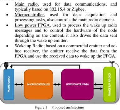
In Figure 1 the proposed architecture is shown. The main elements are:
• Main radio, used for data communications, and typically based on 802.15.4 or Zigbee.
• Microcontroller, used for data acquisition and processing tasks, also controls the main radio element. • Low power FPGA, used to process the wake up radio
messages and to control the hardware of the node depending on the content, it also drives the data sent through the wake up emitter.
• Wake up Radio, based on a commercial emitter and ad-hoc receiver, the emitter receive the data from the FPGA and use the received data to wake up the FPGA.
Both the wake up radio and the low power FPGA blocks are described deeply in the following subsections.
A. Wake up radio 1) Emitter.
In the emitter a commercial chip will be used. The main characteristic for a suitable emitter are:
• Low power static consumption
• Simple modulation (preferred OOK or ASK), in order to facilitate the implementation of the demodulator. • It has to be able to work in an ISM band (868 or 915
MHz).
• Direct access to the data transmission line, in order to avoid the implementation of complex hardware blocks in the FPGA (i.e. a SPI controller).
Finally the TX6001 [17], from RF Monolithics, has been chosen. Its main characteristics are:
• 0.7 uA in sleep mode. • 12 mA when transmitting.
• OOK and ASK modulation supported. • 868.35 MHz carrier frequency. • 2,7 to 3.5 Volts, power supply voltage. • Direct connection to the TX port.
• 20 kbits per second in OOK transmission
The chosen transmitter has the minimum requirements for a Wake up emitter; low power consumption, one of the typical modulation for WuRs, low voltage supply and transmission in a ISM band.
If after real test the distance achieved will not be long enough, a RF amplifier could be included between the antenna and the transmitter but this will impact negatively on the power consumption of the WuR.
2) Receiver.
In the receiver side there are several implementations in the state of the art. Finally, the one presented in [11] has the best performance in power consumption using discrete components and is used as a starting point in the receiver side; at this moment, this solution is chosen to implement the receiver, waiting for future improvements.
The structure of the receiver is based on 3 stages. The first stage, antenna, impedance matching and RF filter for the transmission frequency. The second stage is composed by a voltage multiplier as amplifier and an envelope detector. The last stage is a digitizer stage based on an ultra low power comparator to convert the signal, and also to limit the input voltage in the FPGA, as is shown in Figure 2.
Figure 2 Receiver structure
The reported power consumption for the receiver based on the Figure 2 is 1,2 uW.
B. Actel IGLOO Low power FPGA.
The Low power FPGA family chosen is the ACTEL IGLOO. Nowadays these family devices are the lowest power consumption FPGAs in the market; they are also non-volatile, which is interesting for low power applications.
Igloo FPGA has 6 different power modes
1) Active, the hardware inside FPGA is working.
2) Static, the main clock is deactivated; two different power modes are available.
a) Idle, with the main clock off. In this mode the static power is the only one consumed.In this power mode a faster wake up but with higher power consumption is obtained. Combinational logic is still enabled. The power consumption depends on the static power consumption of the hardware, the Core voltage (VCC)
and the core current (IDD). This current depends
mainly on the size of thedevice (see TABLE II. ).
TABLE II. CORE CURRENT IN IDLE MODE IDD
Device size (Thousand equivalent gates) Core
Voltage 15 30 60 125 250 400 600 1000 Units
1.2 V 4 4 8 13 20 27 30 44 µA
1.5 V 6 6 10 18 34 51 72 127 µA
b) Flash*Freeze (FF) Mode. This is an ultra-low static power mode to reduce power consumption while preserving the state of the registers, SRAM contents and I/O states without switching off any power supplies, inputs, or input clocks. The FF mode needs 1 µs to switch from active state to freeze state, and vice versa. The FF mode can be managed in two ways, using a dedicated pin in the FPGA or routing the pin internally to the FPGA core and state management hardware. The second method enables the design to perform important activities before allowing the device to enter in FF mode, such as transitioning into a safe state, completing the processing of a critical event, etc.
3) Sleep; in this mode, the core voltage and programming voltage are grounded resulting in the turn off of the FPGA core reducing the power consumption. The drawn current is limited to the minimal leakage current. The typical timing characteristics of this mode are tsleep and twakeup of
50 µs. But it also depends on the core voltage.
The following section analyzes the interface of the FPGA with the elements of the architecture, paying special interest to the interface with the Wake up Radio.
V. INTERFACE WAKE UP RADIO -LOW POWER FPGA The main issue that has not been addressed yet is the mechanism to wake up the FPGA from the Wake up Radio side. This point will be addressed in this section. This task can be solved in different ways the most relevant will be described below.
The simplest approach is the one without using the low power modes of the FPGA, while the node is waiting for a RF
FILTER
VOLTAGE
wakeup call. This is not a valid scenario because the power consumption introduced by the “always on” FPGA is too high.
For a simple implementation based on a Manchester encoder/decoder for the data transmissions, a 16 bits address decoder, a 16 bits command decoder and a Simple Finite State machine for basic control tasks in the smallest FPGA has an estimated power consumption of 158 µW. This value is the average power consumed by the FPGA, it is a theoretical value and probably, in a real implementation this value will be higher. By itself it is higher than the desired consumption for the whole WuR. This factor leads to the rejection of the “always on” scheme.
The next scheme is based in the idle mode of the FPGA. In this mode the main clock for all the synchronous blocks of the FPGA remain inactive, and only the combinational blocks are active. In this way the power consumption is reduced mainly because there is no activity of the synchronous elements.
In order to activate the clock an asynchronous preamble detector is implemented. This block counts the time of the preamble; if the detected time is long enough it activates the synchronous blocks.
In this kind of system, the use of a clock control block is mandatory. This implies the use of larger FPGAs, the smaller ones do not have clock control hardware integrated. Because of this, the power consumption in low power modes increases. The smaller device with PLL integrated is the AGL060, (60.000 equivalent gates).
This scheme presents a big drawback due to the usage of the clock control block. This block by itself has power consumption on the range of mW (depending on the number and frequency of the clocks). For the implementation shown in Figure 3, the estimated values are: Pactive= 2,2 mW, Piddle=57
µW, and an average power (5% active, 95% idle) Paverage=164
µW which is also out of the range. To get an acceptable solution the active time should be 1% or lower (Paverage=78
µW).
Finally, the most energy efficient approach is achieved using the Flash* Freeze mode available. In this operation mode, the FPGA is awaken by a wake up message, once it is active, it decodes the message, takes the necessary actions
(wake up the micro, send and acknowledge, etc) and when everything is done, it goes back to the Flash*Freeze mode. Using this scheme the most important task is how to defrost the FPGA. Different ways to wake up the FPGA can be embraced.
The simplest approach is to use the first bit of the message, this mechanism will increase the power consumption of the system because the FPGA will be active much more times than if a mechanism to avoid undesired wake ups is used. In the present work this is the used mechanism, but the next step will be focused on avoiding this false wakeups.
The proposed solutions are the following.
Using a simple timer in order to detect a long preamble before the message; this avoids false wake ups caused by interference, noise or false calls. The main problem is how to get a simple timer that does not introduce too much power consumption in the system. The discrete components available on the market have unacceptable power consumptions.
Other possibility is to send a tuned tone on a known frequency; in this way if the filter is selective enough it can detect the tone and unfreeze the FPGA. This is a promising possibility, but the generation of low frequency signals on the emitter could present a problem that has not been addressed yet. The main advantage of this option is the possibility of tune the wake up filter at different frequencies for the nodes in a known range; this could introduce selectivity in the wake up message if the deployment of the nodes has been properly planned.
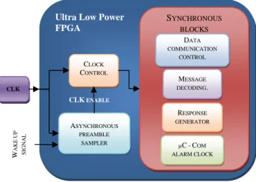
All these schemes are based on the same FPGA architecture, with very simple blocks inside. This allows the use of smaller devices that besides need less resources, i.e., without Clock Management Block, and can reduce power consumption, in the different modes of the FPGA (Flash*Freeze and running), but with the same speed and defined functionalities. Figure 4 shows the basic blocks inside of the FPGA. The estimated power consumption of the FPGA in this scenario is: Smallest device usable, AGL20 (20.000 equivalent gates), Pactive= 0.263 mW, Piddle=9 µW, and an
average power (5% active, 95% idle) Paverage=21 µW. This is
the lowest power consumption of the evaluated solutions, and also the most simple in terms of hardware usage.
Ultra Low Power FPGA
DATA
COMMUNICATION CONTROL
MESSAGE
DECODING.
RESPONSE GENERATOR
µC-COM ALARM CLOCK
CLK
W
AKE UP
SI
GNAL
Ultra Low Power FPGA
ASYNCHRONOUS
PREAMBLE SAMPLER
CLOCK
CONTROL
SYNCHRONOUS
BLOCKS
MESSAGE
DECODING.
RESPONSE GENERATOR
µC-COM ALARM CLOCK
DATA
COMMUNICATION CONTROL
CLK
W
AKE UP
SI
GNAL
CLK ENABLE
VI. CONCLUSIONS
In this paper, the usage of low power FGPAs to implement a complete Wake up Radio for Wireless Sensor Networks has been evaluated.
The theoretical results obtained for power consumption and system speed are interesting and motivate the real implementation of the presented architecture to measure the actual performance of the system.
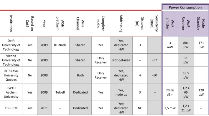
As can be seen in Table III the proposed solution has the best power consumption compared with the based on CotS and very competitive with the other alternatives taking into account the capabilities introduced with the usage of an ultra low power FPGA. This is also the first implementation of WuR based on FPGA.
TABLE III. WUR RADIOS PLATFORMS
Power Consumption
Institution
Based
on
CotS
Year
WSN
platform
WuR
Channel
Complete
radio
Addressin
g
Distance
(m)
Se
nsitivity
(dBm
)
WuR
Emitter
WuR
Re
ce
ive
r
Node
Standby
Delft University of
Technology
Yes 2009 BT‐Node Shared Yes
Yes, dedicated
HW
3
3 mW
801 µW
171 µW
Vienna University of
Technology
No 2009
Shared
Only
Receiver Not detailed ‐‐ ‐57
11
µW
LRTS Laval University Quebec
No 2009
Both
Only Receiver
Yes, dedicated
HW
4 ‐50
18.5
µW
RWTH Aachen University
Yes 2009 TelosB Dedicated Yes Yes,
node µc 3 ‐‐
20.56 dBm
1.2 + 65 µW
120 µW
CEI‐UPM Yes 2011 ‐‐ Dedicated Yes
Yes; dedicated
HW
NC 2,5 mW 1,2 +
21 µW ‐‐
[1] J. Rabaey, M. J. Ammer, J. L. da Silva, D. Pattel and S. Roundry. “PicoRadio Supports Ad Hoc Ultra-Low Power Wireless Networking”. Computer, vol.33, no.7, pp.42-48, July 2000.
[2] G. Anastasi, M. Conti, M. di Franchesco, A. Passarella. “Energy conservation in wireless sensor networks : A survey”. Ad Hoc Networks, vol. 7, pp. 537-568, 2009.
[3] L. van Hoesel. and P. Havinga. “A light weight medium access protocol (LMAC) for wireless sensor networks”. 1st international
workshop on networked sensing systems (INSS2004). Tokyo, Japan, 2004.
[4] V. Rajendran, K. Obraczka and J. Garcia-Luna-Acebes. “Energy-efficient, collision-free medium access control for wireless sensor networks”. 1st ACM conference on embedded networked sensor systmes (SenSys‘03). Los Angeles, CA, USA, November 2003 [5] S. Coleri-Ergen and P. Varaiya. “PEDAMACS: Power efficient and
delay aware medium access protocl for sensor networks” IEEE Transactions on Mobile Computing, vol 5, no 7, pp 920-930. (2006). [6] J. Polastre, J. Hill, and D. Culler. “Versatile low power media access
for wireless sensor networks”. Proceedings of the 2nd international conference on Embedded networked sensor systems (SenSys '04). New York, NY, USA, 95-107.
[7] W. Ye, j. Heideman and D. Estrin. “an energy-efficient MAC protocl for wireless sensor networks”. 21st conference of the IEEE computer and communicaciotns societes (INFOCOM), vol. 3, pp 1567-1576, New York, NY, USA June 2002.
[8] T.V. Dam and K. Langedoen. “An adaptive energy efficent MAC protocl for wireless sensor networks”. 1st ACM confenrece on
Embedde Networked Sensor Systems (SenSys’ 03). Los Angeles, CA, USA, November 2003
[9] L. Gu, and J. A. Stankovic. “Radio-Triggered Wake-Up for Wireless Sensor Networks”. Real Time Systems, vol. 29, pp. 157-182, 2005. [10] A Artés Rodriguez and F. Pérez González. “Comunicaciones
Digitales”. Edited by Pearson -España, ISBN: 9788483223482, 2007. [11] I. Demirkol, C. Ersoy, and E. Onur. "Wake-Up Receivers for
Wireless Sensor Networks: Benefits and Challenges." IEEE Wireless Communications, pp. 88-96, 2009.
[12] B. van der Doorn, W. Kavelaars, and K. Langendoen. "A prototype low-cost wakeup radio for the 868 MHz band." International Journal on Sensor Netwoks 5, no.1 , pp 22-32, 2009.
[13] BT-Node brochure, [online] available:
http://www.btnode.ethz.ch/Documentation/BTnodeRev3HardwareRef erence
[14] J. Ansari, D. Pankin, and P. Mähönen. “Radio-triggered Wake-ups with Addressing Capabilities for Extremely low Power Sensor Network Applications”. International Journal of Wireless Information Networks vol.16, no. 3,pp. 118-130, 2009.
[15] Polastre, J.; Szewczyk, R.; Culler, D.; , “Telos: enabling ultra-low power wireless research”. Fourth International Symposium on Information Processing in Sensor Networks, pp. 364- 369, April, 2005.
[16] .Actel Igloo user guide, [online] available
http://www.actel.com/documents/IGLOO_UG.pdf
[17] TX6001 datashet, [online] available: