Electrical, structural and optical properties of ZnO thin films grown by pulsed laser deposition
12
0
0
Texto completo
(2) https://cimav.repositorioinstitucional.mx/jspui/ The simultaneous occurrence of high optical transparency (>80%) in the visible region and high electrical conductivity (>103 S-cm-1) is not possible in an intrinsic stoichiometric material. Partial transparency and good conductivity can be achieved in thin films of a variety of materials. The easy option to obtain good transparent conductors is to create electron degeneracy in wide band gap oxide materials by controlling the nonstoichiometry or by adding dopants. These conditions can conveniently be created in oxides of indium, tin, zinc, cadmium and their alloys in thin film form. The unique property of the transparent conducting oxide films make them very useful in a large number of electric and optoelectronic applications such as resistors, electromagnetic shield coatings, transparent electrodes for solar cells, antireflection coatings, heat reflecting mirrors, gas sensors and protective coatings. The electrical and optical properties of these films depend mainly on the microstructure, stoichiometry and the nature of impurities present. It also depends on the deposition condition, substrate temperature and oxidation process that occur during and after the deposition. Each deposition technique has characteristic parameters which must be optimized to yield desirable properties. Doping is the most significant parameter which affects the electrooptical properties of the transparent conductor oxides (TCO). The large conductivity of oxide thin film is due to high electron concentration resulting from the deviation from the stoichiometry and doping effects. The deviation in stoichiometry is due to the anion vacancies and excess interstitial electrons. Zinc oxide (ZnO) is an n-type semiconductor with a wide band gap of 3.3 eV, it shows high optical transmittance and a wide range of electrical conductivity values simultaneously. ZnO is used in many different application in both microelectronic and. 2.
(3) https://cimav.repositorioinstitucional.mx/jspui/ optoelectronic devices. As a consequence of it direct energy gap, ZnO absorbs ultraviolet (UV) radiation due to band-to-band transitions (Norton et al., 2004). Furthermore ZnO can be used as semiconducting gas sensor (Subramanyam et al., 2000) due to conductivity changes it exhibits when exposed to oxidizing gases such as ozone. Several techniques can be used to grow ZnO thin film, like pulsed laser deposition (PLD) (Villanueva et al., 2006), ion plating, spray pyrolysis (Olvera et al., 2007), metalorganic chemical vapor deposition (Tan et al., 2005), rfand-dc magnetron sputtering, among others. Due to intrinsic and extrinsic defects, also it is possible with PLD technique to obtain ZnO films with a wide range of resistivity, from 10-4 to 109) cm (Ondo-Ndong et al., 2003). The properties of ZnO thin films are known to depend on deposition parameters such as substrate temperature (Li et al., 2003), type of substrate (Ondo-Ndong et al., 2003), pressure and gas atmosphere (Tvarozek et al., 2007) and thickness (Bouderbala et al., 2008). In particular the growth behavior including growth orientation (Zhang et al., 2007), microstructure and electrical properties (Gao and Li, 2004) of oxide films is very sensitive to the oxygen partial pressure (PO2) used. Therefore, when one attempts to grow ZnO films of high quality using PLD, it is necessary to simultaneously consider both defect formation and film growth behavior in optimizing ambient PO2 in the growth chamber. In the present work, studies have been made on the physical characteristics of ZnO thin films. These films have been grown by using PLD in a vacuum coating chamber. We report results concerning the effect of oxygen partial pressure on the electrical, structural and optical properties of ZnO thin films. Experimental procedure. 3.
(4) https://cimav.repositorioinstitucional.mx/jspui/ Non-stoichiomteric ZnO (ZnO1-δ) thin films (71-22 nm thick) were deposited on glass substrates (Corning No. 7059) using a Nd:YAG laser λ=1064 nm, 10 ns full width at half maximum at a repetition rate of 5 Hz under the conditions listed in Table I. The laser was focused through a 50 cm focal length lens onto a rotating target at a 45° angle of incidence. The targets were prepared from solid reaction of ZnO powder to sintered one solid disk of 5 mm of thickness and diameter of 15 mm. The films were deposited at substrate temperature (Ts) of 300°C in PO2 ranging between 10 and 40 mTorr. The substrates were cleaned in an ultrasonic cleaner for 10 min with acetone and then methanol. The structural properties were determined by measurements in the grazing incidence geometry with an inclination of 1° in the x-ray diffraction beam (XRD) by using CuKα wavelength monochromatic radiation (l=1.5405 Å). Acquisition conditions were: a beam of 40 kV with 35 mA and with an aperture diaphragm of 0.2 mm, using a D5000 Siemens X-ray diffractometer. The thickness (d) of the films was measured by a surface profilometer Dektak-8, Veeco. The electrical properties were determined at room temperature by Van der Pauw-Hall method. For a uniform thickness, the electrical resistivity (ρ) can be determined using the relation ρ = RSd, where RS is the sheet resistance. All sheet resistance and resistivity values were also determined as the average of three measurements of three different films deposited at same conditions. The optical transmittance measurements were carried out using visible near-IR spectrophotometer equipment. The band gap (EG) was determined by extrapolating the straight regions from plots of the square of the absorption coefficient α2 versus photon energy (hv) (Tauc et al., 1966).. 4.
(5) https://cimav.repositorioinstitucional.mx/jspui/ Results and discussion The resistivity of the TCO film depends strongly on the chamber oxygen pressure as well as the stoichiometry of the film (Miller and Haglund, 1966). Oxygen provides the background gas necessary for the optimal PLD growth of complex oxides, and equilibrates the energetic species of the emerging atomic/ionic constituents ablated from the target (Zheng and Kwok, 1993). This can be explained by the nature of PLD. In PLD, the surface of the substrate is covered by atoms and ions pulsed from the target. It has been found that laser-generated atom and ion beams travel toward the substrate with a time duration of about 10 ps and with peak velocities of ~106 cm/s (Zheng et al., 1989). Different atomic species travel at different speeds. However, these velocities eventually equilibrate due to the many collisions between fast and slow atoms. These collisions take place between energetic atoms and the ambient O2. The film stoichiometry is directly related to the velocity distributions of various atoms (Wu et al., 1999). When the densities of various atoms on the substrate surface are uniform and the coverage rates are the same, there is a much better chance of forming a stoichiometry compound. At low oxygen pressures, although the same species leave the target, the density of various species will not be uniform when they arrive on the surface of the substrate and it is most favorable the non-stoichiometry compound. In general, electron conduction in the n-type oxide semiconductors is generated from interstitial or substituted cations and/or vacancies (Chopra et al., 1983). At the optimal PO2 range of 10 to 40 mTorr, energetic atoms and ions with a uniform velocity distribution of various species, combine to produce nonstoichiometric ZnO and produce oxygen vacancies and/or interstitial cations. Figure 1 shows a plot of the electrical. 5.
(6) https://cimav.repositorioinstitucional.mx/jspui/ properties as a function of oxygen deposition pressures for ZnO1-δ thin films at room temperature. As can be see in Table 1, ZnO1-δ compounds are more favorable in the PO2 between 10 to 40 mTorr, the electrical resistivity decrease from ρ~1.1x10⁻¹ Ω-cm at 10 mTorrr reaching a minimum value of ρ~2.1x10⁻² Ω-cm. The mechanism responsible for the conductivity changes in ZnO1-δ thin films is the formation and annihilation of oxygen vacancies. To films grown in these range of PO2 (10 to 40 mTorr), the average Hall coefficient, measured by Van der Pauw electrode configuration, gave around of −0.61 cm3C−1, suggesting that the conduction is n-type. Combining the Hall coefficient and conductivity measurements resulted in an average carrier density of n~9.6x1019 cm−3 and average Hall mobility of the electrons of ~8.6 cm2V−1s−1 as can see in the Figure 1. The obtained XRD patterns for the ZnO1-δ thin films are shown in Figure 2 at different PO2. The XRD patterns of the films are consistent with the pattern of ZnO powder reported in standard JCPDS data file and show a preferred growth orientation along the c-axis, that is, (002) plane, which is perpendicular to the substrate. The lattice constants of these films are calculated from the obtained values of d-spacing and their corresponding (hkl). The average values of the lattice constants are found to be (a = b = 3.24 Å and c = 5.23 Å) which are close to the standard value of hexagonal form of ZnO powder. The PO2 doesn't affect the main peaks positions, which reflect the existence of ZnO single phase. Five principal peaks (100), (002), (101), (110) and (103) are appeared in the films. The intensities of these planes are increased gradually by increasing of the PO2 still to 30 mTorr. In contrast the film grown at 40 mTorr, these. 6.
(7) https://cimav.repositorioinstitucional.mx/jspui/ intensities of the peaks are decreased. The crystal size of ZnO1-δ thin films were calculated using Scherrer formula:. Where D is the mean grain size, β is the full width at half maximum of the diffraction line in radians, θ is the diffraction angle and λ is the wave length of X-ray (1.542 Å). The crystal size and volume of the unit cell of the films grown are shown in Table 2 as function of the PO2. The average of the grains size was about 16.76 nm. The average of the volume of the ZnO1-δ unit cell was approximately 47.71 Å3 while the standard volume of the ZnO unit cell reported is 47.63 Å3. These indicate an expansion in the ZnO1-δ unit 7.
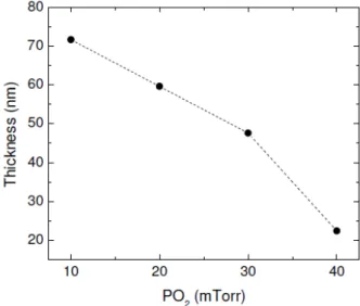
(8) https://cimav.repositorioinstitucional.mx/jspui/ cell as a consequence of the annihilation of oxygen vacancies (VO) in the lattice and the interstitials sites formation. However, the film deposited at PO2 = 30 mTorr shown a minor volume of the unit cell than the ZnO powder, by indicating a compression of the unit cell due at the VO formation. From Figure 3, we can see that the thickness of the films decrease from 71 to 22 nm as increasing of the PO2 this reduction can be attributed primarily to collision of the ablated Zn and oxygen particles with the ionized gas plasma during deposition. The transmittance versus wavelength for the ZnO1- δ thin films is shown in Figure 4 at different PO2. It is observed that the films are highly transparent with sharp absorption edge at λ = 380 nm (UV region) and average transmittance of ~85%. The optical band gap values are obtained from the plot (α hv )2 vs hv by extrapolating the linear portion of the plot to (α hv )2 = 0. The inset in Figure 4 shows the optical band gap for ZnO1- δ thin films at 30 mTorr, similar results were measurements in the others films. The calculated optical band gap has no change with PO2; its average value is ~3.3 eV.. 8.
(9) https://cimav.repositorioinstitucional.mx/jspui/. Conclusion Electrical, structural and optical properties of nostoichiometric ZnO (ZnO1-δ) thin films grown by Nd:YAG pulsed laser deposition were studied in function of the PO2 in the range of 10 to 40 mTorr. The electrical resistance of the ZnO1-δ thin films decreases with the oxygen pressure reaching a minimum resistance of ρ∼2.1x10⁻² Ω-cm at 30 mTorr. The increase/decrease of the electrical resistance is ascribed to the annihilation/ formation of the oxygen vacancies (VO) complex defects. XRD patterns showed the existence of hexagonal ZnO single phase and the optical transmittance in the VIS range of the ZnO1-δ thin films, shown an average transmittance of ~85% with optical band gap of average value of ~3.3 eV. Acknowledgments The authors would like to thank Oswaldo Gómez, Mario Herrera, Daniel Aguilar, and Wilian Cauich for technical assistance, also to Mrs. Lourdes Pinelo for secretarial assistance. This work has been supported under Project No. 59996 CONACYT/México.. 9.
(10) https://cimav.repositorioinstitucional.mx/jspui/ E. Chan y Díaz acknowledges also CONACyT/México for his scholarship in the Advanced Materials Research Center, (CIMAV), from Chihuahua, National Laboratory of Nanotechnology at CIMAV and Partial Financial support: Secretaría de Educación Pública, PRONABES/632/2010, México. CONACYT/México. References Norton DP, Heo YW, Ivill MP, Ip K, Pearton SJ, Chisholm MF, Steiner T (2004). ZnO: growth, doping and processing. Mater. Today, 7: 34-40. Subramanyam TK, Naidu BS, Uthanna S (2000). Physical Properties of Zinc Oxide Films Prepared by dc Reactive Magnetron Sputtering at Different Sputtering Pressure. Cryst. Res. Technol., 35: 1193-1202. Villanueva YY, Liu DR, Cheng PT (2006). Pulsed laser deposition of zinc oxide. Thin Solid Films, 501: 366-369. Olvera M, de la L, Gómez H, Maldonado A (2007). Doping, vacuum annealing, and thickness effect on the physical properties of zinc oxide films deposited by spray pyrolysis. Sol. Energy Mater. Sol. Cells, 91: 1449-1453. Tan ST, Chen BJ, Sun XW, Hu X, Zhang XH, Chua SJ (2005). Properties of polycrystalline ZnO thin films by metal organic chemical vapor deposition. J. Cryst. Growth, 281: 571-576. Ondo-Ndong R, Ferblantier G, Al Kalfioui M, Boyer A, Foucaran A (2003). Properties of RF magnetron sputtered zinc oxide thin films. J. Cryst. Growth, 255: 130135.. 10.
(11) https://cimav.repositorioinstitucional.mx/jspui/ Ondo-Ndong R, Pascal-Delannoy F, Boyer A, Giani A, Foucaran A (2003). Structural properties of zinc oxide thin films prepared by r.f. magnetron sputtering. Mater. Sci. Eng. B., 97: 68-73. Tvarozek V, Novotny I, Sutta P, Flickyngerova S, Schtereva K, Vavrinsky E (2007). Influence of sputtering parameters on crystalline structure of ZnO thin films. Thin Solid Films, 515: 8756-8760. Bouderbala M, Hamzaoui S, Amrani B, Reshak Ali H, Adnane M, Sahraoui T, Zerdali M (2008). Thickness dependence of structural, electrical and optical behaviour of undoped ZnO thin films. Phys. B, 403: 3326-3330. Zhang JP, He G, Zhu LQ, Liu M, Pan SS, Zhang LD (2007). Effect of oxygen partial pressure on the structural and optical properties of ZnO film deposited by reactive sputtering. Appl. Surf. Sci., 253: 9414-9421. Gao W, Li Z (2004). ZnO thin films produced by magnetron sputtering. Ceram. Int., 30: 1155-1159. Tauc J, Grigorovici R, Vancu A (1966). Optical Properties and Electronic Structure of Amorphous Germanium. Phys. Status Solidi., 15: 627-637. Miller JC, Haglund RF (1998). Laser Ablation and Desorption, Academic press, San Diego, CA,, pp. 544-551. Zheng JP, Kwok HS (1993). Low resistivity indium tin oxide films by pulsed laser deposition. Appl. Phys. Lett., 63: 1-3. Zheng JP, Ying QY, Witanachchi S, Huang ZQ, Shaw DT, Kwok HS (1989). Role of the oxygen atomic beam in low temperature growth of superconducting films by laser deposition. Appl. Phys. Lett., 54: 954-956.. 11.
(12) https://cimav.repositorioinstitucional.mx/jspui/ Wu Y, Maree CH M, Haglund Jr RF, Hamilton JD, Morales Paliza MA, Huang MB, Feldman LC, Weller RA (1999). Resistivity and oxygen content of indium tin oxide films deposited at room temperature by pulsed-laser ablation. J. Appl. Phys., 86: 991994. Chopra KL, Major S, Pandya DK (1983). Transparent conductors-a status review. Thin Solid Films, 102: 1-46.. 12.
(13)
Figure
Documento similar
Click here to view linked References.. The most important point defects and defect complexes have been explored and intrinsic defect formation energies were determined [21]. To
These surface states lie in the bulk energy gap of thin topological insulators.In thin topological insulator films tunnelling between top and bottom sur- face opens a finite gap in
In particular, all the defects discussed above play a key role in streamlining the physical and chemical properties of semi- conductor materials directly associated with the
Therefore to characterize and study possi- ble evolution effects of the structural and dynamical properties of ELOs, we describe their three dimensional distributions of mass
However, the sulfurization temperature is the parameter that regulates the formation of an orthorrombic single phase SnS thin film with the optimum properties to be used
The films that exhibit p-type behavior are the films grown at lower temperatures. At the same time, the thin films obtained at these temperatures present also a
influence of these parameters on the size and distribution of Te inclusions, deep defects, optical and electrical properties of CdZnTe detectors. In the fourth chapter, the effect
Since the oxide growth rate is approximately constant along the transformation process, the oxidation time scales linearly with the nitride thickness.. This property enables
