Discerning recombination mechanisms and ideality factors through impedance analysis of high efficiency perovskite solar cells
40
0
0
Texto completo
(2) Abstract The ubiquitous hysteresis in the current-voltage characteristic of perovskite solar cells (PSCs) interferes in a proper determination of the diode ideality factor ( n ), a key parameter commonly adopted to analyze recombination mechanisms. An alternative way of determining n is by measuring the voltage variation of the ac resistances in conditions of negligible steady-state dc currents. A reliable analysis of n based on the determination of the resistive response, free of hysteretic influences, reveals two separated voltage exponential dependences using different perovskite absorbers (3D perovskites layer based on CH3NH3PbI3 or mixed Cs0.1FA0.74MA0.13PbI2.48Br0.39) and a variety of interlayers (2D perovskite thin capping). The dominant resistive element always exhibits an exponential dependence with factor n 2 , irrespective of the type of perovskite and capping layers. In addition, a non-negligible resistive mechanism occurs at low-frequencies (with voltage-independent time constant ~1 s) which is related to the kinetic properties of the outer interfaces, with varying ideality factor ( n 2 for CH3NH3PbI3, and n 1.5 for Cs0.1FA0.74MA0.13PbI2.48Br0.39). Our work identifies common features in the carrier recombination mechanisms among different types of high-efficiency. PSCs,. and. simultaneously. signals. particularities. architectures, mostly in the carrier dynamics at outer interfaces.. 2. on. specific.
(3) Keywords Perovskites solar cells Recombination Impedance spectroscopy Capacitance 2D capping. 3.
(4) 1. Introduction Over the last few years perovskite solar cells (PSCs) gained great attention in the field of photovoltaics with an unprecedented increase in power conversion efficiency (PCE) for facile solution processing [1-4]. Currently, the main challenge in order to reach commercialization in the perovskite solar research lies in fabricating high efficient perovskite-based devices exhibiting good long-term stability under real operation conditions. In order to fulfill these ambitious goals, investigations on materials science are mainly focused on three directions: (i) development of new stable light harvesting perovskites alternatives to CH3NH3PbI3 (MAPI), (ii) engineering selective charge extracting materials and (iii) optimization of fabrication processes/materials quality. Furthermore some specific applications such as flexible photovoltaics [5, 6], tandem cells [7, 8] and light emitting devices [9, 10] are also of potential interest. However, despite progressive improvements are systematically reported, there is still a lack of comprehension on important physical aspects ruling the device performance [11]. Several standard characterization protocols and tools used in photovoltaics present difficulties when applied to PSCs because of the occurrence of anomalous behaviors which prevent typical interpretations. The ubiquitous hysteresis in the current densityvoltage ( J V ) curve has forced the definition of good practices in order to properly report photovoltaic parameters [12, 13]. The presence of slow relaxation processes (from milliseconds to minutes) causes different measured J V curves depending on the bias sweep direction, scan rate, illumination and polarization history [11, 14]. This makes it difficult to report on PCE as well as on any other parameter calculated from the. J V curve as diode ideality factor and resistance, and the same applies to most transient measurements. 4.
(5) Ideality factor ( n ) has been traditionally adopted as an indicating parameter of the carrier recombination processes dominating the solar cell operation. However, its analysis from J V curves has resulted inconclusive [15] for PSCs because of the mentioned masking contributions of hysteretic currents. Apart from open-circuit dependence on light intensity and temperature, and electroluminescence analyses [15], an alternative way of determining the diode ideality factor is by measuring the voltage variation of alternating current (ac) resistances in conditions of negligible steady-state direct currents (dc). Differential resistances are no more than current derivatives with respect to voltage perturbations in such a way that recombination losses and ideality factors distinctively appear by analyzing resistances as well. This is feasible by performing impedance measurements in open-circuit conditions under varying illumination intensities following a well-established protocol. Several works have drawn upon the relative contribution of bulk and outer interface carrier recombination routes on the overall performance of PSCs [15-19]. It has been specifically suggested that a transition occurs from bulk- to interface-dominated recombination when pristine solar cells experience ionic contact polarization upon cycling [16]. For less performing or degraded PSCs, interfaces seem to play a determining role on carrier recombination [20]. The issue is however open in the case of high-efficiency PSCs as those investigated in this work. We develop here a reliable analysis of the ideality factors (exponents of the photovoltage dependence) based on the determination of the resistive response, free of hysteretic interferences. Two separated voltage exponential dependences are revealed using different perovskite absorbers (3D perovskites layer based on CH3NH3PbI3 or mixed Cs0.1FA0.74MA0.13PbI2.48Br0.39) and a variety of interlayers (2D perovskite thin 5.
(6) capping), with distinctive exponents: (i) the dominant resistive element acting in the high-frequency range always exhibits an exponential dependence with ideality factor n 2 , irrespective of the type of perovskite and capping layers. (ii) A non-negligible. resistive mechanism occurs at low-frequencies (with voltage-independent time constant ~1 s) related to the kinetic properties of the outer interfaces. Here the exponent exhibits two. extreme. cases,. namely. n2. for. CH3NH3PbI3-. and. n 1.5. for. Cs0.1FA0.74MA0.13PbI2.48Br0.39-based solar cells, with a strong correlation with the concomitant huge capacitance, which attains values up to the order of mF cm -2 under 1 sun illumination. Our work allows progressing in the identification of common features in the carrier recombination mechanisms among different types of high-efficiency PSCs while signaling particularities on specific architectures, particularly in the carrier dynamics at outer interfaces. Note that Table S1 summarizes symbols and abbreviations in order to facilitate the reading of our results and discussion. 1.1. Background A simple parameterization for hysteretic/capacitive effects was proposed that include large displacement currents J cap of capacitive origin and non-capacitive hysteretic contributions J non cap (e.g. reactivity) in a constant evolution with time. The total measured dc current includes both terms added to the operational current J oper as [21, 22]. J (V ) J oper (V ) J cap (V ) J non cap (V ). (1). .. Concerning J oper , the most common approximation neglecting parasitic series 6.
(7) resistances Rs (which will be our case here at open-circuit condition) considers the difference between recombination current J rec and generation current J ph as. qV V J ph J oper (V ) J rec (V ) J ph J s exp 1 n k T R B sh . (2). with J ph being the photocurrent (zero in dark), J s is the saturation current, Rsh the shunt resistant, q the elementary charge and kBT the thermal. This later parameter is of upmost importance in order to identify the processes ruling recombination. It is of general acceptance from the ideal Shockley equation [23, 24]. that n values. approaching 1 indicate band-to-band recombination in the quasi-neutral region, whilst n near to 2 means recombination throughout mid-gap centers in the depletion region following the Shockley-Read-Hall (SRH) theory [25, 26]. Although n lies between 1 and 2 mostly, some other effects like surface recombination and non-uniform recombination centers, mainly in heterojunction devices, can include variations or more exotic results as summarized in Table S2. Importantly, in the core of these analysis n is defined by the position and symmetry of the separation of the quasi-Fermi levels of electrons and holes E Fn and E Fp , respectively, which ultimately define the output voltage as qV E Fn E Fp For the determination of n more than 20 different methods can be found in literature [27], most of them using the single-exponential diode model, dc regime and forward bias from a single J V data set. More recently, specifically on PSCs [15], the use of dark. J V. curves, short-circuit current vs. open-circuit voltage at different. illuminations ( J sc Voc ) as well as the use of electroluminescence analyses have been suggested. In this regard, it is useful to generalize the bias-dependent ideality factor 7.
(8) from Eqs. (1)-(2) by neglecting J cap and J non cap , assuming dark condition ( J ph 0 ) and a V range so J V / Rsh J s and dJ / dV Rsh , hence taking the logarithm 1. derivative after some operations, see Eqs. (S1)-(S3), 1. q dJ n(V ) J V k BT dV .. (3). Similarly, J ph can be measured at short-circuit ( J sc ) and the corresponding Voc can be taken at open-circuit for a sequence of illumination intensities. Thus, considering Rsh large enough that J ph Voc / Rsh J s and dJ ph / dVoc Rsh , the bias-dependent 1. ideality factor can be extracted (see Eqs. S4-S5 in the SI) from the J sc Voc plot of results as. dJ ph (Voc ) q n(Voc ) J ph (Voc ) kBT dVoc . 1. (4). .. The ideality factors defined by Eqs. (3) and (4) may accord in the ranges where all the considered approximations are valid, if electronic reciprocity is obeyed [28, 29]. Interestingly, the definition of n as from Eq. (3). is directly proportional to the. recombination resistance per unit area, which also can be obtained from Eq. (2) with two contributions in parallel (assuming voltage-independent photo-generation), namely Rsh and Rrec as. Rrec (V ) . qV nk BT exp qJ s nk B T .. (5). The resulting total dc resistance is presented in Eq. (S6). It is evident that by substituting Eqs. (1) and (2) in (3), a constant n is expected. In any case, the evaluation of n can be 8.
(9) accessed from the measurement of the resistance. In the case of deviation from a single exponential n (V ) . q dV R V k BT R V . (6). where the integration limits may ensure the above specified. Note that despite the equations for n V can be used for the particular estimation of. n at a given V , our approach here will be more interested in getting n from the exponential trends of the resistance. However the determination of such exponential trends from the J V characteristics (or from R (V ) calculated from J V curves) can be problematic in practical terms due to the presence of Rseries , J cap and J non cap effects which are typically enhanced as dc currents increases. The above limitations can be overcome by the use of the impedance spectroscopy (IS) measurements at open-circuit under different illumination intensities. This experiment, which has been earlier conducted in several photovoltaic technologies [3033], consists in setting the cell at the forward bias V at which J rec equals J ph , i.e. open-circuit, and then measuring the IS spectrum upon a small ac perturbation in a given frequency ( f ) window. The spectra are modeled with suitable equivalent circuits and resistance is obtained for each illumination and corresponding Voc . Importantly, in PSCs the applied V should not be trusted from the Voc value reported from J V curves due to the hysteresis effects. Instead, direct Voc chrono-voltammetries should be monitored for ensuring zero dc currents at the given illumination intensity before IS measuring. This last procedure eliminates the repercussion of transient currents, either originated by capacitive or non-capacitive hysteretic mechanisms. 9.
(10) 2. Experimental 2.1. Fabrication of MAPI-based devices Conductive FTO glass (NSG10) was sequentially cleaned by sonication in a 2 % Helmanex solution and isopropanol for 15 min respectively. A 20-50 nm titania blocking layer was applied on the substrates by spraying a solution of titanium diisopropoxide bis(acetylacetonate) in ethanol at 450 °C.. For the 200-300 nm. mesoporous TiO2 layer, 30 NR-D titania paste from Dyesol diluted in ethanol (150mg/ml) was applied by spin-coating at 4000 rpm for 10s followed by a sintering step at 500 °C for 20 min. After cooling down the substrates a Li-treatment was applied by spin-coating 60 µl of a solution of Tris(bis(trifluoromethylsulfonyl)imide) (Li-TFSI) in acetonitrile (10mg/ml) onto the mesoporous layer, followed by a sintering step at 500 °C for 10 min to decompose the Li-salt as previously described [34]. The 3D MAPI perovskite layers were fabricated by a single step spin-coating procedure reported by Seok et al. [35] (Fig. 1a-d). For the perovskite precursor solution 484 mg of PbI2(TCI) and 159 mg methylammonium iodide (Dyesol) were dissolved in 800 µl dimethyl sulfoxide (DMSO). For the 2D perovskite on the titania side (Fig. 1b,d) 2mol% of 5-Ammonium valeric acid (5-AVAI) was added to the perovskite precursor solution. The perovskite solution was spun at 4000 rpm for 30s using a ramp of 2000rpms-1. 10s prior to the end of the spin-coating sequence 100 µl chlorobenzene were poured onto the spinning substrate. Afterwards the substrates were transferred onto a heating plate and annealed at 100 °C for 45 min. To form a thin layer of 2D perovskite on top of the perovskite capping layer (Fig. 1c,d) the samples were cooled down and a solution of benzimidazolium iodide (BI) in isopropanol (5 mg/ml) was dynamically spin-coated onto the perovskite layers at 3000 rpm. The samples were afterwards 10.
(11) annealed for additional 10 minutes at 100 °C. The hole-transporting material, spiro-OMeTAD (Merk) was applied from a 70mM solution in chlorobenzene. Tert-butylpyridine (Tbp), Tris(2-(1H-pyrazol-1-yl)-4-tertbutylpyridine)cobalt(III) (FK209) and Li-TFSI were added as additives. 330 mol% Tbp, 50 mol% Li-TFSI from a 1.8M stock solution in acetonitrile and 3 mol% FK209 from a 0.25M stock solution in acetonitrile was mixed to the spiro-OMeTAD solution. The final HTM solution was spin-coated dynamically onto the perovskite layers at 4000rpm for 20s. The gold electrodes were deposited by thermal evaporation of 80 nm gold using a shadow mask under high vacuum conditions. 2.2. Fabrication of mixed perovskite-based devices FTO glass substrates (NSG) were sequentially cleaned with the hellmanex solution, acetone, and ethanol. Thus a compact TiO2 layer was coated on the FTO substrate heated by spray pyrolysis deposition at 450°C. A precursor solution was a diluted titanium diisopropoxide (Sigma-Aldrich) in ethanol (0.6 ml: 10 ml). After cooling, mesoporous TiO2 film (~200 nm) was prepared coating a diluted TiO2 paste (Dyesol 30 NR-D) solution in ethanol. Right after spin-coating, the substrates were sintered on a hot plate at 500°C for 20 min. For doping Li on TiO2, films were treated with 0.1 M Lithium bistrifluoromethanesulfonimidate solution (Li-TFSI, Aldrich) in acetonitrile by spin-coating at 5000 rpm for 10 s, and sintered again at 500°C for 30 min. Subsequently, a 3D perovskite solution (Fig. 1e-g) was prepared by mixing FAI (1.1 M), PbI2 (1.15 M), MABr (0.2 M) and PbBr2 (0.2 M) in a mixed solvent (DMF: DMSO = 4: 1 volume ratio). Another solution of CsPbI3 was also prepared as 1.15 M in DMF: DMSO (same volume ratio). And then, (FAPbI3)0.85(MAPbBr3)0.15 and CsPbI3 solutions were mixed as 10 vol% ratio. The solution was then spin-coated at 2000 rpm for 10 s 11.
(12) and continuously at 5000 rpm for 30 s in nitrogen glove box. After entering the second step, 100 μL of anhydrous trifluorotoluene was poured at 15 seconds before the finish. Films were then annealed at 100°C for 60 min. For forming additional 2D perovskite film on top of this perovskite film, and between TiO2 and CFMPIB, (Fig. 1f,g) substrates were treated with a PEAI isopropanol solution. 100 μL of PEAI solution (15 mg/ml) were spin-coated on the TiO2 substrate or the as-prepared perovskite films at 4000 rpm, and annealed at 100°C for 5 min. Finally, Spiro-OMeTAD was spin-coated at 4000 rpm for 20 s. The 70 mM SpiroOMeTAD solution was prepared by dissolving in chlorobenzene with 4-tertbutylpyridine, Li-TFSI in acetonitrile, and Co[t-BuPyPz]3[TFSI]3 (FK209) in acetonitrile at the molar ratio of Spiro:FK209:Li-TFSI:TBP of 1:0.03:0.5:3.3. Devices were completed with a thermal evaporation of 70 nm thickness gold rear electrode. 2.3. Characterization All electrical characterizations were carried out at room temperature and atmosphere (humidity bellow 10%). For the impedance analysis and the J-V curve bias sweep monitoring an SP-200 BioLogic potentiostat was used. For standard PCE evaluation a AAA solar simulator from Newport equipped with a 1000 W Xenon lamp was employed while a dc regulated Illuminator from Oriel Instruments was used for tuning. Voc as the light intensity was varied.. 3. Results In. this. work. we. analyzed. PSCs. with. the. structure. FTO/TiO2. (compact)/TiO2(mesoporous)/perovskite/spiro-OMeTAD/Au. The devices comprise a 3D. perovskite. layer. based. on. CH3NH3PbI3 12. (MAPI). or. mixed.
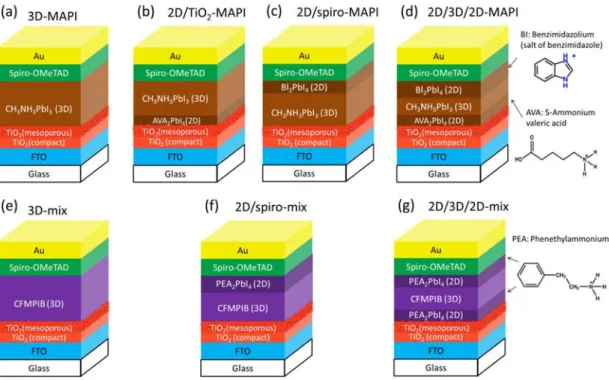
(13) Cs0.1FA0.74MA0.13PbI2.48Br0.39 (CFMPIB) as reference samples (cells labeled 3D-MAPI and 3D-mix with structures as those shown in Fig. 1a,e, respectively). In addition, MAPI-based variants were measured (Fig. 1b-d) in which 2D perovskite thin capping was included with AVA2PbI4 between TiO2 and MAPI, and/or Bl2PbI4 between MAPI and spiro-OMeTAD. Similarly, CFMPIB variants included PEA2PbI4 as a thin coating at both interfaces (Fig. 1f, g). With these cells we conducted J V measurements in dark and under illumination, as well as IS measurements at open-circuit with different light intensities, as previously described. The data of IS were fitted to equivalent circuit models. Based on the resulting resistive and capacitive behaviors, differences in the recombination features between the 3D perovskite type and the presence of 2D capping at the interfaces were found.. Fig. 1. Scheme of structures of layers composing the studied devices with corresponding labeling. Scaling between layers thicknesses was not considered and the corresponding organic molecules composing the 2D perovskites are highlighted in (d).. 13.
(14) Our characterization program included the sequenced measurement of J V curves (fresh) under standard, one sun illumination and IS measurements at open-circuit under different illumination intensities. After that, which takes around 5 hours of continuous biasing changes and illuminations, the samples were left in dark around 12 hours, at ambient conditions (~295 K and ~10% humidity), and their J V curves (stressed) were subsequently measured again. The objective of this protocol is to evaluate potential degradation effects. The illuminated J V. characteristics before (fresh) and after (stressed) the. characterization routine for a set of MAPI- and CFMPIB-based samples are presented in Fig. S1. Among fresh curves it can be observed that the selected ensemble presented no significant performance variations. On the contrary, it is evident that the presence of the 2D layers favored the degradation in MAPI based cells, while an apparent stability is found for all mixed perovskite samples. It might result from the 2D perovskite layer that protects the mixed perovskite layer and their rigid property under humid and illuminated conditions [36, 37]. Specifically, a significant loss in fill factor (FF) of around 70% of the PCE is observed for 2D/MAPI devices. On the other hand, the decrease of PCE in mix-perovskite samples and MAPI samples without 2D layer did not exceed 10% of initial values, in agreement with our previous study [38]. These data are summarized in Table S3 where corresponding performance parameters: Voc , J sc , FF and PCE can be found, as well as the PCE ratio between fresh and stressed samples. On the MAPI cells these results seems to contrast with our previous findings [39] where the stability was remarkably improved when including 2D capping layers.. 14.
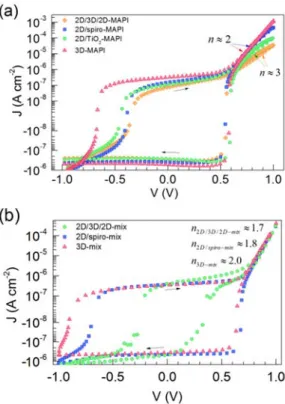
(15) 3.1. Jcap effects and n values from dark curves It is important to highlight that in photovoltaic responses shown in Fig. S1 are only. J V curves by sweeping the bias in the direction from open-circuit to short-circuit. The discussion on the efficiencies on the sweep direction and corresponding stability can be found in recent previous works [39]. Nevertheless, in this sense the basic measurement of dark J V curves at both scan directions is included [21, 40, 41]. Dark J V hysteretic curves are illustrated in Fig. 2 where typical capacitive square patterns are observed, pointing to the presence of an approximately constant capacitance C in reverse and low forward bias regimens [21]. Accordingly, one can take J cap s C , being s the voltage scan rate, and the estimated capacitances result in the order of. μF cm2 , which match the low-frequency capacitance values extracted from dark impedance, as discussed in the next section. Slight capacitive differences appeared between MAPI-based samples (Fig. 2a), while no evident J cap dissimilarities were detected for the CFMPIB-based samples (Fig. 2b) [42].. 15.
(16) Fig. 2. Dark J V curves of (a) MAPI- and (b) CFMPIB-based samples. The curves were -2 -1 measured at a scan rate of s 100 mV s resulting in J cap 0.1 0.4 A cm (. C 1.0 4.0 F cm-2 ) and J cap 0.4 A cm -2 ( C 4.0 F cm-2 ) for (a) and (b), respectively.. Differences between MAPI samples and similarities between CFMPIB cells are also evidenced towards the region of high injection currents. Here, the ideality factor can be extracted from the exponential response following Eq. (2). MAPI-based cells without interlayers (or comprising spiro-OMeTAD/Bl2PbI4 interlayer) in Fig. 2 (a), and CFMPIB-based cells in Fig. 2b exhibit similar ideality factors, around 2. However, the two structures comprising TiO2/AVA2PbI4 in MAPI-based cells (Fig. 2a) showed ideality factors even larger than 3. These two later cases also included the presence of small inverted hysteresis between 0.5 V and 1.0 V, which suggest a complex interplay of non-capacitive effects and/or changes in the capacitance itself. The differences in 16.
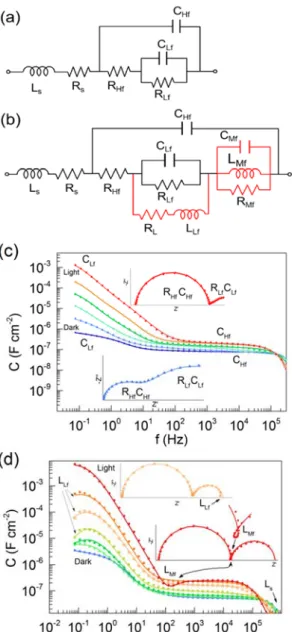
(17) exponential laws are better illustrated in Fig. S2c,d where the dc resistance was obtained following the current derivative on the average dc currents of Fig. 2a,b J V curves. Also by using the definition of Eq. (3), n (V ) can be obtained as displayed in Fig. S2e,f. Following the relationship between recombination mechanisms summarized in Table S2 and their corresponding ideality factors extracted from J V curves, we might understand the behavior of 3D-MAPI, 2D/spiro-MAPI and CFMPIB-based samples (. n 2 ) as indicative of large generation-recombination processes in the depletion region involving both minority and majority carriers. This agrees with the nearly voltageindependent capacitance extracted at reverse and low forward bias (Fig. S2a,b), suggesting a fully depleted quasi-intrinsic perovskite layer forming a p-i-n heterojunction. Actually, it is known that p-i-n diodes operate in the high-injection condition ( n 2 ) and hence recombination is within the i-region [43]. One would then expect that the classical model of application for these devices is that of a p-i-n diode with dispersion in the ideality factor possibly due to non-capacitive effects including series resistances. The latter effects could be behind behaviors for those samples including the interphase TiO2/AVA2PbI4, i.e. 2D/TiO2-MAPI and 2D/3D/2D-MAPI, where n is significantly larger than 2. Contrastingly, the exponential slopes were not so scattered in mixed perovskite based samples with 2D capping. This would be a second hint pointing to the predominance of bulk recombination in CFMPIB-based samples in comparison to the larger importance of interfaces in MAPI cells. 3.2. Impedance spectroscopy analysis IS analysis was carried out in each of the above analyzed samples. Complete spectra with respective modeling are presented in Fig. S3,S4 for MAPI- and CFMPIB-based samples, respectively. The employed equivalent circuits are those of Fig. 3a,b and 17.
(18) illustrative capacitance and impedance spectra are displayed in Fig. 3c,d for different illumination intensities in open-circuit conditions. For MAPI cells the used equivalent circuit is drawn in Fig. 3a where Ls and Rs are series inductive and resistive elements (related to wires and connections), respectively. The core of the circuit is composed by two couples of resistive-capacitive (RC) elements in matryoshka configuration. At frequencies higher than 100 Hz, the capacitance spectra describe a plateau around a value CHf , and for almost all illumination intensities a clear arc of diameter RHf is observed in the impedance plots. However, as frequency is decreased below 100 Hz, capacitance is significantly enhanced towards a second plateau around CLf in the Bode plots and a second arc RLf is evident in the impedance plot. The equivalent circuit in Fig. 3a, is probably the most reported model for describing IS spectra in PSCs because of its simplicity and physical meaning [20, 44, 45]. In general CHf and RHf have been identified with dielectric and recombination properties, while the origin of CLf and RLf , although still are under debate, has been associated with the slow mechanisms of accumulation capacitance that also produce the hysteretic currents in the J V curves [11, 41, 46]. It is already known that recombination properties of the TiO2/absorber interfaces largely depend on specific preparation routes and processing conditions. For instance, the use of ammonia [47] or engineering of hierarchical microstructures [48] alters the TiO2 surface states and concomitant electronic structure with evident changes in interface recombination. In contrast, for CFMPIB-based cells the model of Fig. 3b for the analysis of IS spectra results more featured. Two main sets of elements have been highlighted in red. First, affecting the lowest frequencies, an inductive element LLf with series resistance 18.
(19) RL are shunting CLf and RLf . These elements can produce a decrease of capacitance in the Bode plot or a distortion from a semicircle in impedance plot (see Fig. 3d). On the other hand, at intermediate frequencies extra resistance RMf , capacitor C Mf and inductor LMf are needed for properly fitting the patterns that can even produce loops in the impedance plot (see Fig. 3d) and a concave in the capacitance Bode representation. The greater complexity of the equivalent circuit for CFMPIB-based samples should be related with the diverse composition of the light harvesting material in comparison with MAPI cells. It could be thought that a more important contribution of defects takes place in the mixed perovskites which result extreme in the 2D/3D/2D-mix sample. More importantly, the observation of inductive loops has been related in previous papers to complex recombination/extraction mechanisms occurring in the vicinity of the outer interfaces [14, 44, 49, 50].. 19.
(20) Fig. 3. Equivalent circuits for modeling IS spectra of (a) MAPI- and (b) CFMPIB-based samples. At Voc and different illumination intensities, some capacitance (Bode plot) and impedance (Nyquist plot) are illustrated for the 2D/3D/2D configurations in (c) and (d) for MAPI- and CFMPIB-based samples, respectively. Also in (c) the main capacitive and resistive elements effects are highlighted while in (d) the considered inductor elements are pointed as their influence. See complete spectra in Fig. S3-S4.. The main resistive and capacitive parameters (namely CLf , RLf , CHf and RHf ) 20.
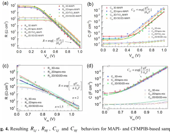
(21) determined from fits are presented in Fig. 4. Corresponding general behaviors in PSCs have been earlier reported in the literature [20, 51] and here we present an illustrative phenomenological modeling (solid lines in Fig. 4) based on the recombination resistance in Eq. (5) in parallel with Rsh , and for the capacitances following the empirical form. qV C C0 C1 exp oc kBT . (7). where , C0 and C1 serve as fitting parameters. Specifically, is an exponential coefficient, C0 is a ground capacitance and C1 C0 is such way that C C0 in dark. At low frequency, we notice that CLf exhibits the exponential trend of Eq. (7) with. 2 for MAPI-based cells that result in C1, MAPI 400 pF cm -2 , resulting in large capacitive values CLf 100 mF cm -2 at Voc 1.0 V . In the case of CFMPIB-based devices, 1.5 and CLf 10 mF cm -2 results one order lower than for MAPI samples at Voc 1.0 V , which implies that C1,mix 60 fF cm -2 in Eq. (7). In both cases a value around of order 10 μF∙cm-2 is extracted for C0 that points to the occurrence of electrode polarization caused by ionic double layers, as introduced in previous papers [41] that also agrees with the capacitive currents reported in Fig. 2. Regarding high-frequency capacitive responses, CHf behavior in Fig. 4b,d is nearly constant at forward bias around the geometric capacitance. CHf Cg C0 ,. proportionally to the expected thicknesses of the perovskite layers, as earlier commented on Fig. S2a,b. Only a slight increase is found towards larger forward biases that hardly fit an exponential law. Such minor CHf augment could be originated by thermal effects after prolonged illumination [52], and it will be carefully studied in 21.
(22) future works. High-frequency resistance RHf is understood in terms of Eq. (5) as previously discussed. At low forward bias (i.e. 0.1 V) the ac resistances in Fig. 4a,c seems to be in the same order that dc resistances obtained from dark J V curves in Fig. S2c,d, and associated to shunts. However, above 0.6 V an exponential decrease was found with different trends among the samples. For the CFMPIB-based samples n was found to be between 1.5-2.0 for all the samples, while for MAPI cells the IS shows a predominant trend around n 2 . Furthermore, RHf is the dominant resistor at forward bias. This allows identifying RHf as the dominant operational recombination resistance. Comparing exponential trends (extracted from IS analysis) with the results from dark. J V curves, CFMPIB samples also deliver lower n values than MAPI cells. However, overestimation of n does not occurs here provided that IS analysis excludes. Rs effects in the RHf evaluation. Once more, as summarized in Table S2, MAPI cells seem to be dominated by SRH recombination in the depletion zone ( n 2 ), whilst for CFMPIB samples ( n 2 ) the influence of band to band recombination current in a quasi-neutral region could be expected. More explicitly, by using Eq. (6) the ideality factors can be obtained as presented in Fig. S5. In addition in Fig. S6 are presented the normalized J ph in logarithm scale vs. Voc , that also confirm the ideality factors around 2 and 1.5 for MAPI and CFMPIB cells, respectively, by using Eq. (4).. 22.
(23) Fig. 4. Resulting RLf , RHf , CLf and CHf behaviors for MAPI- and CFMPIB-based samples, as indicated, from the fitting of IS spectra at different illumination intensities through opencircuit regime (Fig. S3-S4).. 4. Discussion The results shown in previous sections confirm that CFMPIB samples exhibit lesser n values than MAPI cells. Our IS approach, by measuring in open-circuit conditions. under varying light intensity, seems to provide more reliable n values than those inferred from J V curves in which the capacitive currents certainly complicate the analysis. Although resistances determined by IS can be easily interpreted in terms of known recombination mechanisms accounting for the operation of inorganic photovoltaic technologies, perovskite solar cells present a distinctive capacitive feature in the low-frequency wing of the spectra (Fig. 4b,e). A huge increase of capacitance that grows with illumination and charge injection up to mF cm -2 (under 1 sun light or 1.0 23.
(24) V) has been measured and connected to the hysteretic features and surface/interface phenomena [20, 21, 40-42, 51]. This is indeed a prominent issue that also correlates with the resistive behavior which exhibits the same exponential trends with voltage (Fig. 4). In order to provide a coherent picture about the perovskite solar cell functioning, it is necessary to integrate the large low-frequency capacitive feature into a comprehensive model. Nonetheless, it should be noticed that a suitable model may include, in addition to possibly ion-related mechanisms, a strong component which considers the photogenerated electronic charge. A recently introduced approach has connected the huge photo-capacitance to the accumulation of carriers in the vicinity of the outer interfaces. Only one analytical model has been proposed based on the appearance of space-charge accumulation zones of majorities at the contacts [43], kinetically driven by the slow displacement of ionic species [51]. This surface accumulation capacitance (SAC) Cs presents an exponential coefficient ( 2 ) with respect to the voltage built at the accumulation zone Vs (see Eq. (S7) and corresponding explanatory comments). Vs incorporates a significant part of the photovoltage in such a way that the CLf exp qVoc / 2k BT experimental trend observed for MAPI-based PSCs in this work, which corroborates the voltagedependence previously reported for less-performing cells [20, 53]. However, the SAC model is not able to reproduce the case of CFMPIB-based cells with 1.5 . It would imply a doping or trap states’ profile at the junction, being the relation between Vs and. Voc dependent on particularities of the interface. On the other hand, capacitance increments following an exponential law with Voc has been typically understood in terms of chemical capacitances C , which are known to 24.
(25) account for bulk charging of density of states. For carrier occupancy of conduction and valence band states following the Boltzmann statistics, one can calculate the bulk chemical capacitance (BCC) per unit area [30, 54]. and also the edge chemical. capacitance (ECC) confined at the interfaces (see Eqs. (S8)-(S15) and corresponding explanatory comments). Assuming a bulk origin for the low-frequency capacitance, and noticing that resistive and capacitive responses are highly correlated (exhibiting in Fig. 4 the same exponent), it is feasible to reproduce the CLf exp qVoc / k BT trends. The exponent 2 for MAPI-based cells agrees with an intrinsic bulk absorber in a p-i-n model, while 1.5 for CFMPIB-based cells points to a medium injection regime in a p-n cell. However, due to the low intrinsic carrier density ( ni 105 cm-3 for MAPI considering parabolic band approximation with effective conduction and valence band carrier densities around 1018 cm-3 [55, 56] and band-gap E g 1.6 eV ) the theoretical expectations cannot match the actual values attained by the low-frequency capacitance (see Fig. S8) [11, 57]. Obviously, further theoretical analyses are still needed here for clarifications, but note that whatever the mechanism behind CLf is, it is strongly constricted by a slow relaxation time constant (subsequently commented), possibly connected to the ionic kinetics. This, for instance, prevent the probably chemical capacitance to affect CHf , in excess of Cg , at frequencies typically above 1 kHz [52]. Anyway, regardless of the chemical or dielectric electronic nature of CLf , its correlation with ionic processes seems to be a fact, as tackled in several studies also referring the. J V curve hysteresis phenomena [11]. These ionic mechanisms could be behind the large photo-generated CLf , so they should be considered in subsequent theoretical 25.
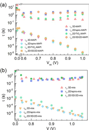
(26) approaches. Accordingly, the assumptions and approximations made in order to match models and experiments are illustrated in Fig. S8 and the above mentioned models are compared in Table S4. In any case our approaches entail the importance of interfaces as the locus explaining the operating mechanisms in PSCs [51, 58, 59]. An alternative way of approaching recombination features is by examining the response times from IS measurements. The corresponding high-frequency characteristic time calculated from the circuit elements as Hf RHf CHf is presented in Fig. 5, showing clear exponential decrease (following the resistor dependence on voltage) in the range from milliseconds to microseconds. It results approximately identical for all MAPI cells and only a little shifted toward larger Hf values for the 2D/3D/2D-mix sample among the CFMPIB-based cells. This characteristic time cannot be regarded as a true carrier lifetime because the high-frequency capacitance is related to the geometrical capacitance, as explained previously. It is then a response time coupling dielectric (capacitive) and recombination (resistive) elements. On the other hand, a very slow process with characteristic time Lf RLf CLf. ,. approximately constant within the order of seconds (see Fig. 5), is responsible for the IS patterns at low frequencies. For higher illumination and consequently larger J ph , the process remains almost unaltered in time scale (see Fig. 5), and since more current flows 1 ( RLf J ph ) more charge is stored ( CLf J ph ), as evidenced from exponential slopes. in Fig. 4b,d and Fig. S6. Response times of the order of seconds were previously identified by us using IS with less performing PSCs [20, 53]. Similar trends are now verified using high-efficiency perovskite solar cells. As discussed previously [20], a constant (illumination-intensity independent) response time is a strong indication that 26.
(27) electronic mechanisms originating capacitance and resistance should be inherently coupled. But again the time constant corresponding to the low-frequency mechanism cannot be considered a true carrier lifetime because the chemical nature of the capacitive process is not assured.. Fig. 5. Resulting Lf and Hf behaviors for MAPI- and CFMPIB-based samples, as indicated, from the fitting of IS spectra at different illumination intensities through open-circuit regime (Fig. S3-S4).. Nevertheless, here we also highlight the possible connection between the ideality factor, from resistances and photocurrents, and the exponential coefficient of CLf . In case of pure chemical capacitance the exact match n is expected [43], while in our case a general trend n was found. More importantly, regarding the physical meaning in MAPI-based cells, n 2 suggest stronger surface dominant recombination, which 27.
(28) is in agreement with the change of Lf in Fig. 5a as the thin film 2D capping layers were included. Particularly, it seems that including Bl2PbI4 towards the hole-selective contact increases the relaxation time. On the other hand, in the CFMPIB-based samples,. n 1.5 suggest stronger bulk dominant recombination, which agree with the nearly constant Lf in Fig. 5b, independently of the presence of thin film 2D capping layers.. 5. Concluding Remarks Our impedance analysis of different 3D perovskite absorbers (CH3NH3PbI3 or mixed Cs0.1FA0.74MA0.13PbI2.48Br0.39) and 2D perovskite interlayers (AVA2PbI4, Bl2PbI4, and PEA2PbI4) allow identifying common patterns and dissimilarities. We can say that (i) the dominant resistive elements (high-frequency) behave for both set of samples following an exponential dependence on voltage with n 2 , slightly lower in the case of CFMPIB-based cells. The simpler interpretation is connecting this resistance to the recombination mechanism within the absorber bulk. However, it cannot be completely discarded that outer interfaces actively participate in the carrier recombination determining R Hf values. Concerning the low-frequency behavior, it is demonstrated that (ii) exponential indexes vary differently as a function of the absorber type: again n 2 for MAPI-based cells, but n 1 .5 in the case of CFMPIB-based cells. This dissimilar behavior leads us to consider the low-frequency response as exclusively originated at the outer interfaces which are modified in our experiments by several interlayers. Moreover, (iii) the very origin of the low-frequency resistance is still elusive. It can be either connected to localized interfacial recombination processes or to carrier transport mechanisms across 28.
(29) the interfacial space-charge zone. Finally, (iv) it is proved here that the interfacial kinetics yields, for all the absorbers and contact layers used, a constant (voltageindependent) time constant of the order of seconds, which can be hardly explained by only recalling classical photovoltaic models of transport and recombination in the absorber bulk. In addition, it is observed that MAPI-based cells exhibit simpler interfacial kinetic processes that CFMPIB-based ones. More featured inductive mechanisms appear in the latter case. It should be noted that our analysis on the trends of capacitive and resistive elements upon open-circuit voltage states the repercussion of each solar cell part on the overall functioning, and provides a reliable tool for device analysis and parameter extraction.. Acknowledgments We acknowledge funding from MINECO of Spain under project MAT2016-76892C3-3-R. O.A. acknowledges Generalitat Valenciana for the grant GRISOLIA/2014/035 and SAOT funded by the German Research Foundation (DFG) in the framework of the German excellence initiative. The authors acknowledge SNSF NRP 70 project; number:407040_154056, European Commission H2020-ICT-2014-1,SOLEDLIGHT project, grant agreement N1: 643791 and the Swiss State Secretariat for Education, Research and Innovation (SERI). We thank Borun New Material Technology for providing high quality spiro-OMeTAD.. Appendix A. Supporting information Supplementary data associated with this article can be found in the online version at http://dx.doi.org/10.1016/j.nanoen.2018 29.
(30) References [1] J. Bisquert, E.J. Juárez-Pérez, P.V. Kamat, Hybrid Perovskite Solar Cells: the Genesis and Early Developments 2009-2014, Fundació Scito, Valencia, 2017. [2] M.A. Green, A. Ho-Baillie, H.J. Snaith, The emergence of perovskite solar cells, Nat. Photon., 8 (2014) 506-514. [3] N.-G. Park, M. Grätzel, T. Miyasaka, K. Zhu, K. Emery, Towards Stable and Commercially Available Perovskite Solar Cells, Nat. Energy, 1 (2016) 16152. [4] Y.-K. Ren, X.-H. Ding, Y.-H. Wu, J. Zhu, T. Hayat, A. Alsaedi, Y.-F. Xu, Z.-Q. Li, S.-F. Yang, S.-Y. Dai, Temperature-Assisted Rapid Nucleation: A Facile Method to Optimize the Film Morphology for Perovskite Solar Cells, J. Mater. Chem. A, 5 (2017) 20327-20333. [5] I.K. Popoola, M.A. Gondal, T.F. Qahtan, Recent Progress in Flexible Perovskite Solar Cells: Materials, Mechanical Tolerance and Stability, Renewable Sustainable Energy Rev., 82 (2017) 3127-3151. [6] D.H. Shin, J.H. Heo, S.H. Im, Recent Advances of Flexible Hybrid Perovskite Solar Cells, J. Korean Phys. Soc., 71 (2017) 593-607. [7] P.V. Kamat, Hybrid Perovskites for Multijunction Tandem Solar Cells and Solar Fuels. A Virtual Issue, ACS Energy Lett., 3 (2018) 28-29. [8] M. Anaya, G. Lozano, M.E. Calvo, H. Míguez, ABX3 Perovskites for Tandem Solar Cells, Joule, 1 (2017) 769-793. [9] L. Dou, Y. Yang, J. You, Z. Hong, W.-H. Chang, G. Li, Y. Yang, SolutionProcessed Hybrid Perovskite Photodetectors with High Detectivity, Nat. Commun., 5 (2014) 5404. [10] Y.-H. Kim, H. Cho, J.H. Heo, T.-S. Kim, N. Myoung, C.-L. Lee, S.H. Im, T.-W. Lee, Multicolored Organic/Inorganic Hybrid Perovskite Light-Emitting Diodes, Adv. Mater., 27 (2015) 1248-1254. [11] P. Lopez-Varo, J.A. Jiménez-Tejada, M. García-Rosell, S. Ravishankar, G. Garcia-Belmonte, J. Bisquert, O. Almora, Device Physics of Hybrid Perovskite Solar Cells:. Theory. and. Experiment,. Adv.. 10.1002/aenm.201702772. 30. Energy. Mater.,. (2018). DOI:.
(31) [12] J.A. Christians, J.S. Manser, P.V. Kamat, Best Practices in Perovskite Solar Cell Efficiency Measurements. Avoiding the Error of Making Bad Cells Look Good, J. Phys. Chem. Lett., 6 (2015) 852-857. [13] E. Zimmermann, K.K. Wong, M. Müller, H. Hu, P. Ehrenreich, M. Kohlstädt, U. Würfel, S. Mastroianni, G. Mathiazhagan, A. Hinsch, T.P. Gujar, M. Thelakkat, T. Pfadler, L. Schmidt-Mende, Characterization of Perovskite Solar Cells: Towards a Reliable Measurement Protocol, APL Mater., 4 (2016) 091901. [14] S. Ravishankar, O. Almora, C. Echeverría-Arrondo, E. Ghahremanirad, C. Aranda, A. Guerrero, F. Fabregat-Santiago, A. Zaban, G. Garcia-Belmonte, J. Bisquert, Surface Polarization Model for the Dynamic Hysteresis of Perovskite Solar Cells, J. Phys. Chem. Lett., 8 (2017) 915–921. [15] W. Tress, M. Yavari, K. Domanski, P. Yadav, B. Niesen, J.P. Correa Baena, A. Hagfeldt, M. Graetzel, Interpretation and Evolution of Open-Circuit Voltage, Recombination, Ideality Factor and Subgap Defect States during Reversible LightSoaking and Irreversible Degradation of Perovskite Solar Cells, Energy Environ. Sci., (2017). [16] J.-P. Correa-Baena, S.-H. Turren-Cruz, W. Tress, A. Hagfeldt, C. Aranda, L. Shooshtari, J. Bisquert, A. Guerrero, Changes from Bulk to Surface Recombination Mechanisms between Pristine and Cycled Perovskite Solar Cells, ACS Energy Lett., 2 (2017) 681-688. [17] L. Contreras-Bernal, M. Salado, A. Todinova, L. Calio, S. Ahmad, J. Idígoras, J.A. Anta, Origin and Whereabouts of Recombination in Perovskite Solar Cells, J. Phys. Chem. C, 121 (2017) 9705-9713. [18] J. Jiménez-López, W. Cambarau, L. Cabau, E. Palomares, Charge Injection, Carriers Recombination and HOMO Energy Level Relationship in Perovskite Solar Cells, Sci. Rep., 7 (2017) 6101. [19] N.F. Montcada, J.M. Marín-Beloqui, W. Cambarau, J.s. Jiménez-López, L. Cabau, K.T. Cho, M.K. Nazeeruddin, E. Palomares, Analysis of Photoinduced Carrier Recombination Kinetics in Flat and Mesoporous Lead Perovskite Solar Cells, ACS Energy Lett., 2 (2017) 182−187. [20] I. Zarazua, G. Han, P.P. Boix, S. Mhaisalkar, F. Fabregat-Santiago, I. MoraSeró, J. Bisquert, G. Garcia-Belmonte, Surface Recombination and Collection 31.
(32) Efficiency in Perovskite Solar Cells from Impedance Analysis, J. Phys. Chem. Lett., 7 (2016) 5105-5113. [21] O. Almora, C. Aranda, I. Zarazua, A. Guerrero, G. Garcia-Belmonte, Noncapacitive Hysteresis in Perovskite Solar Cells at Room Temperature, ACS Energy Lett., 1 (2016) 209–215. [22] O. Almora, L. Vaillant-Roca, G. Garcia-Belmonte, Perovskite Solar Cells: A brief Introduction and some Remarks, Rev. Cubana Fis., 34 (2017) 58-68. [23] W. Shockley, The Theory of p-n Junctions in Semiconductors and p-n Junction Transistors, Bell Syst. Tech. J., 28 (1949) 435-489. [24] W. Shockley, Electrons and Holes in Semiconductors, D. Van Nostrand, Princenton, New Jersey, 1950. [25] W. Shockley, W.T. Read, Statistics of the Recombinations of Holes and Electrons, Phys. Rev., 87 (1952) 835-842. [26] R.N. Hall, Electron-Hole Recombination in Germanium, Phys. Rev., 87 (1952) 387-387. [27] M. Bashahu, P. Nkundabakura, Review and tests of methods for the determination of the solar cell junction ideality factors, Solar Energy, 81 (2007) 856863. [28] C. Donolato, A Reciprocity Theorem for Charge Collection, Appl. Phys. Lett., 46 (1985) 270-272. [29] P.P. Boix, A. Guerrero, L.F. Marchesi, G. Garcia-Belmonte, J. Bisquert, Current-Voltage Characteristics of Bulk Heterojunction Organic Solar Cells: Connection Between Light and Dark Curves, Adv. Energy Mater., 1 (2011) 1073-1078. [30] O. Almora, L.G. Gerling, C. Voz, R. Alcubilla, J. Puigdollers, G. GarciaBelmonte, Superior Performance of V2O5 as Hole Selective Contact over other Transition Metal Oxides in Silicon Heterojunction Solar Cells, Sol. Energy Mater. Sol. Cells, 168 (2017) 221-226. [31] G. Garcia-Belmonte, A. Guerrero, J. Bisquert, Elucidating Operating Modes of Bulk-Heterojunction Solar Cells from Impedance Spectroscopy Analysis, J. Phys. Chem. Lett., 4 (2013) 877-886. [32] F. Fabregat-Santiago, J. Bisquert, G. Garcia-Belmonte, G. Boschloo, A. Hagfeldt, Influence of Electrolyte in Transport and Recombination in Dye-Sensitized 32.
(33) Solar Cells studied by Impedance Spectroscopy, Sol. Energy Mater. Sol. Cells, 87 (2005) 117-131. [33] I. Mora-Sero, G. Garcia-Belmonte, P.P. Boix, M.A. Vazquez, J. Bisquert, Impedance spectroscopy characterisation of highly efficient silicon solar cells under different light illumination intensities, Energy Environ. Sci., 2 (2009) 678-686. [34] F. Giordano, A. Abate, J.P. Correa Baena, M. Saliba, T. Matsui, S.H. Im, S.M. Zakeeruddin, M.K. Nazeeruddin, A. Hagfeldt, M. Graetzel, Enhanced Electronic Properties in Mesoporous TiO2 via Lithium Doping for High-Efficiency Perovskite Solar Cells, Nat. Commun., 7 (2016) 10379. [35] N.J. Jeon, J.H. Noh, Y.C. Kim, W.S. Yang, S. Ryu, S.I. Seok, Solvent Engineering for High-Performance Inorganic–Organic Hybrid Perovskite Solar Cells, Nat. Mater., 13 (2014) 897-903. [36] C. Ma, C. Leng, Y. Ji, X. Wei, K. Sun, L. Tang, J. Yang, W. Luo, C. Li, Y. Deng, S. Feng, J. Shen, S. Lu, C. Du, H. Shi, 2D/3D Perovskite Hybrids as MoistureTolerant and Efficient Light Absorbers for Solar Cells, Nanoscale, 8 (2016) 1830918314. [37] Y. Zhou, F. Wang, Y. Cao, J.-P. Wang, H.-H. Fang, M.A. Loi, N. Zhao, C.-P. Wong,. Benzylamine-Treated. Wide-Bandgap. Perovskite. with. High. Thermal-. Photostability and Photovoltaic Performance, Adv. Energy Mater., 7 (2017) 1701048. [38] K.T. Cho, G. Grancini, Y. Lee, E. Oveisi, J. Ryu, O. Almora, M. Tschumi, P.A. Schouwink, G. Seo, S. Heo, J. Park, J. Jang, S. Paek, G. Garcia-Belmonte, M.K. Nazeeruddin, Selective Growth of Layered Perovskite for Stable and Efficient Photovoltaics, Energy Environ. Sci., (2018) in press (DOI: 10.1039/C1037EE03513F). [39] G. Grancini, C. Roldán-Carmona, I. Zimmermann, E. Mosconi, X. Lee, D. Martineau, S. Narbey, F. Oswald, F. De Angelis, M. Graetzel, M.K. Nazeeruddin, OneYear Stable Perovskite Solar Cells by 2D/3D Interface Engineering, Nat. Commun., 8 (2017) 15684. [40] M. Valles-Pelarda, B.C. Hames, I. García-Benito, O. Almora, A. MolinaOntoria, R.S. Sánchez, G. Garcia-Belmonte, N. Martín, I. Mora-Sero, Analysis of the Hysteresis Behavior of Perovskite Solar Cells with Interfacial Fullerene Self-Assembled Monolayers, J. Phys. Chem. Lett., 7 (2016) 4622-4628. [41] O. Almora, I. Zarazua, E. Mas-Marza, I. Mora-Sero, J. Bisquert, G. Garcia33.
(34) Belmonte, Capacitive Dark Currents, Hysteresis, and Electrode Polarization in Lead Halide Perovskite Solar Cells, J. Phys. Chem. Lett., 6 (2015) 1645-1652. [42] O. Almora, C. Aranda, E. Mas-Marzá, G. Garcia-Belmonte, On Mott-Schottky Analysis Interpretation of Capacitance Measurements in Organometal Perovskite Solar Cells, Appl. Phys. Lett., 109 (2016) 173903. [43] S.M. Sze, K.K. Ng, Physics of Semiconductor Devices, 3rd ed., John Wiley & Sons, Hoboken, New Jersey, USA, 2007. [44] A. Guerrero, G. Garcia-Belmonte, I. Mora-Sero, J. Bisquert, Y.S. Kang, T.J. Jacobsson, J.-P. Correa-Baena, A. Hagfeldt, Properties of Contact and Bulk Impedances in Hybrid Lead Halide Perovskite Solar Cells Including Inductive Loop Elements, J. Phys. Chem. C, 120 (2016) 8023–8032. [45] A. Todinova, L. Contreras-Bernal, M. Salado, S. Ahmad, N. Morillo, J. Idígoras, J.A. Anta, Towards Universal Approach to the Analysis of Impedance Spectra of Perovskite Solar Cells. Equivalent Circuits and Empirical Analysis, ChemElectroChem, 4 (2017) 1-12. [46] O. Almora, A. Guerrero, G. Garcia-Belmonte, Ionic Charging by Local Imbalance at Interfaces in Hybrid Lead Halide Perovskites, Appl. Phys. Lett., 108 (2016) 043903. [47] J. Zheng, L.e. Mo, W. Chen, L. Jiang, Y. Ding, Z. Li, L. Hu, S. Dai, Surface States in TiO2 Submicrosphere Films and their Effect on Electron Transport, Nano Research, 10 (2017) 3671-3679. [48] Z.-Q. Li, L.-E. Mo, W.-C. Chen, X.-Q. Shi, N. Wang, L.-H. Hu, T. Hayat, A. Alsaedi, S.-Y. Dai, Solvothermal Synthesis of Hierarchical TiO2 Microstructures with High Crystallinity and Superior Light Scattering for High-Performance Dye-Sensitized Solar Cells, ACS Appl. Mater. Interfaces, 9 (2017) 32026-32033. [49] E. Ghahremanirad, A. Bou, S. Olyaee, J. Bisquert, Inductive Loop in the Impedance Response of Perovskite Solar Cells Explained by Surface Polarization Model, J. Phy. Chem. Lett., 8 (2017) 1402-1406. [50] A. Kovalenko, J. Pospisil, J. Krajcovic, M. Weiter, A. Guerrero, G. GarciaBelmonte, Interface Inductive Currents and Carrier Injection in Hybrid Perovskite Single Crystals, Appl. Phys. Lett., 111 (2017) 163504. [51] I. Zarazua, J. Bisquert, G. Garcia-Belmonte, Light-Induced Space-Charge 34.
(35) Accumulation Zone as Photovoltaic Mechanism in Perovskite Solar Cells, J. Phys. Chem. Lett., 7 (2016) 525-528. [52] O. Almora, C. Aranda, G. Garcia-Belmonte, Do Capacitance Measurements Reveal Light-Induced Bulk Dielectric Changes in Photovoltaic Perovskites?, J. Phys. Chem. C, (2017) in press (DOI: 10.1021/acs.jpcc.1027b11703). [53] I. Zarazúa, S. Sidhik, T. Lopéz-Luke, D. Esparza, E. De la Rosa, J. ReyesGomez, I. Mora-Seró, G. Garcia-Belmonte, Operating Mechanisms of Mesoscopic Perovskite Solar Cells through Impedance Spectroscopy and J–V Modeling, J. Phys. Chem. Lett., 8 (2017) 6073-6079. [54] I. Mora-Seró, Y. Luo, G. Garcia-Belmonte, J. Bisquert, D. Muñoz, C. Voz, J. Puigdollers, R. Alcubilla, Recombination Rates in Heterojunction Silicon Solar Cells Analyzed by Impedance Spectroscopy at Forward Bias and Under Illumination, Sol. Energy Mater. Sol. Cells, 92 (2008) 505-509. [55] E. Menéndez-Proupin, P. Palacios, P. Wahnón, J.C. Conesa, Self-consistent Relativistic Band Structure of the CH3NH3PbI3 Perovskite, Phys. Rev. B, 90 (2014) 045207. [56] G. Giorgi, J.-I. Fujisawa, H. Segawa, K. Yamashita, Small Photocarrier Effective Masses Featuring Ambipolar Transport in Methylammonium Lead Iodide Perovskite: A Density Functional Analysis, J. Phys. Chem. Lett., 4 (2013) 4213-4216. [57] J. Bisquert, G. Garcia-Belmonte, I. Mora-Sero, Characterization of Capacitance, Transport and Recombination Parameters in Hybrid Perovskite and Organic Solar Cells, in: E. Da Como, F. De Angelis, H.J. Snaith, A. Walker (Eds.) Unconventional Thin Film Photovoltaics, The Royal Society of Chemistry, Cambridge, 2016, pp. 57-106. [58] Y. Yang, M. Yang, David T. Moore, Y. Yan, Elisa M. Miller, K. Zhu, Matthew C. Beard, Top and Bottom Surfaces Limit Carrier Lifetime in Lead Iodide Perovskite Films, Nat. Energy, 2 (2017) 16207. [59] B. Wu, H.T. Nguyen, Z. Ku, G. Han, D. Giovanni, N. Mathews, H.J. Fan, T.C. Sum, Discerning the Surface and Bulk Recombination Kinetics of Organic–Inorganic Halide Perovskite Single Crystals, Adv. Energy Mater., 6 (2016) 1600551.. 35.
(36) Osbel Almora graduated in Physics from the University of Havana, Cuba, in 2013 and joined INAM at the Universitat Jaume I of Castelló, Spain, in 2014. He recently continued his pre-doctoral studies joining i-MEET at the Friedrich-Alexander Universität Erlangen-Nürnberg, Germany, in 2017. His main topic of interest is the characterization and modeling of energy devices. Most of his research activities have been focused on all-solid-state photovoltaics, including CdTe, perovskite and silicon solar cells.. Kyung Taek Cho was educated at the Hanyang University where he received a B.S. (2012) and at Korea Advanced Institute of Science and Technology (KAIST) where he received M.S. (2014). He is a Ph.D student at EPFL (2014-present). His main research interests include the design of perovskite solar cells having high efficiency and long term stability. 36.
(37) Sadig Aghazada was born in Azerbaijan. He received his specialist degree in Chemistry from Lomonosov Moscow State University in 2013 working with Dr. Dolzhenko V. D., and the same year started his Ph.D. on cyclometalated ruthenium complexes for dye-sensitized solar cells at EPFL with Prof. Nazeeruddin and Prof. Graetzel. In February 2018, he has obtained his doctoral degree.. Iwan Zimmermann received his Master in Chemistry and Molecular Sciences from Bern University in 2010 and completed a Ph.D. in Inorganic Chemistry at Stockholm University in 2014. Currently he is working as a postdoctoral fellow in the group of Professor Nazeeruddin at EPFL Valais, where his research is focused on the development of perovskite solar cells.. 37.
(38) Gebhard J. Matt received his master degree in Physics in 2000 followed by a Ph.D in Physical Chemistry under the mentorship of Prof. N.S. Sariciftci at the Johannes Kepler University of Linz, Austria in 2005. After’s stay at the local industry and a postdoctoral stay at the Institute for Semiconductor Physic with Prof. G. Bauer, he joined the "Institute Materials for Electronics and Energy Technology" (i-MEET) at the Friedrich Alexander University of Erlangen, Germany, with Prof. C. J. Brabec. His main research activities are on charge-transport investigation of solution processed semiconductors and the detection of high-energetic radiation.. Christoph J. Brabec received his PhD (1995) in Physical Chemistry from Linz University, Austria joined the group of Alan Heeger at UC Santa Barbara (USA) for a sabbatical. He joined the SIEMENS research labs (project leader) in 2001, Konarka in 38.
(39) 2004 (CTO), Erlangen University (FAU - Professor for Material Science) in 2009, ZAE Bayern e.V. (scientific director and board member) in 2010 and became the spokesmen of the Interdisciplinary Center for Nanostructured Films (IZNF) in 2013. His research interests include all aspects of solution processing organic, hybrid and inorganics semiconductor devices with a focus on photovoltaics and renewable energy systems.. Prof. Mohammad K. Nazeeruddin current research at EPFL focuses on Perovskite and Dye Sensitized Solar Cells, and Light-emitting diodes. He has published more than 560 peer-reviewed papers, ten book chapters, and inventor/co-inventor of over 75 patents. Nazeeruddin has been named Thomson Reuters "Highly Cited Researcher" and one of the 19 scientists identified as The World's Most Influential Scientific Minds 2016 and 2017 from all scientific domains. He has appeared in the ISI listing of most cited chemists and has more than 71'000 citations with an h-index of 125. He was appointed as World Class University professor and Adjunct Professor at the King Abdulaziz University, Jeddah, elected to the European Academy of Sciences and Fellow of The Royal Society of Chemistry.. 39.
(40) Germà Garcia-Belmonte joined the Universitat Jaume I de Castelló in 1992 and currently works as a Full Professor of Applied Physics (2010) at the Institute of Advanced Materials (http://www.inam.uji.es/). He conducts experimental and theoretical research on materials and devices for production and storage of clean energies, in particular, on electronics and ionics of energy devices. He is currently active in the topic of perovskite-based solar cells and lithium-ion batteries. Device physics using impedance spectroscopy is his main expertise.. Author Osbel Almora Kyung Taek Cho Sadig Aghazada Iwan Zimmermann Gebhard J. Matt Christoph J. Brabec Mohammad K. Nazeeruddin Germà Garcia-Belmonte. ORCID 0000-0002-2523-0203 0000-0002-7419-1415 0000-0002-7568-4481. 0000-0002-9440-0253 0000-0001-5955-4786 0000-0002-0172-6175. 40.
(41)
Figure
+2
Documento similar
One might expect that there is a smooth transition between a small sample regime, in which finite size effects such as those observed in sums of heavy-tailed random variables,
In the preparation of this report, the Venice Commission has relied on the comments of its rapporteurs; its recently adopted Report on Respect for Democracy, Human Rights and the Rule
The draft amendments do not operate any more a distinction between different states of emergency; they repeal articles 120, 121and 122 and make it possible for the President to
H I is the incident wave height, T z is the mean wave period, Ir is the Iribarren number or surf similarity parameter, h is the water depth at the toe of the structure, Ru is the
Subjects classified as altruistic using linear conditional-contribution profile methodology should be classified as altruistic using personal cost undertaken by
The purpose of the research project presented below is to analyze the financial management of a small municipality in the province of Teruel. The data under study has
In our proposal we modeled the problem using a Markov decision process and then, the instance is optimized using linear programming.. Our goal is to analyze the sensitivity
In addition to simulation, Petri nets can be analyzed [Mur89], for example regarding reachability (whether the net can reach a certain marking), boundedness (whether the number
