DOI 10.1007/s12034-016-1282-z
Growth and properties of lead iodide thin films by spin coating
D ACUÑA1, B KRISHNAN1,2,∗, S SHAJI1,2, S SEPÚLVEDA1,2and J L MENCHACA3
1Facultad de Ingeniería Mecánica y Eléctrica, Universidad Autónoma de Nuevo León, San Nicolás de los Garza, Nuevo
León 66455, México
2Universidad Autónoma de Nuevo León, Centro de Innovación, Investigación y Desarrollo de Ingeniería y Tecnología,
Apodaca, Nuevo León 66600, México
3Facultad de Ciencias Físico Matemáticas, Universidad Autónoma de Nuevo León, San Nicolás de los Garza, Nuevo León
66455, México
MS received 19 July 2015; accepted 21 March 2016
Abstract. In this study, lead iodide (PbI2) thin films were deposited on glass substrates by spin coating a solution of 0.2 M PbI2dissolved in dimethylformamide, varying the deposition time and the spin speed. The thickness of the thin films decreased with increase in spin speed and deposition time, as examined by profilometry measurements. The structure, morphology, optical and electrical properties of the thin films were analysed using various techniques. X-ray diffraction patterns revealed that the thin films possessed hexagonal structures. The thin films were grown highly oriented to [001] direction of the hexagonal lattice. Raman peaks detected at 96 and 136 cm−1were corre-sponding to the characteristic vibration modes of PbI2. The X-ray photoelectron spectroscopy detected the pres-ence of Pb and I with core level binding energies corresponding to that in PbI2. Atomic force microcopy showed smooth and compact morphology of the thin films. From UV–Vis transmittance and reflectance spectral analysis, the bandgap of the thin films∼2.3 eV was evaluated. The dark conductivity of the thin films was computed and the value decreased as the deposition time and spin speed increased.
Keywords. Lead iodide thin films; spin coating; structure and morphology; XRD; Raman spectrum.
1. Introduction
Lead iodide (PbI2) belongs to the layered semiconductor
family, and is a widely studied semiconductor for various applications such as X-ray detectors [1], medical imaging [2], nuclear detection [3] and photosensitivity semiconductor-metal applications [4]. It has also been used as a precursor for obtaining the methylammonium lead iodide perovskite-based solar cell [5], one of the highest solution-processed solar cells reported so far. Lead iodide exists in hexagonal crystalline structure having an intrinsic bandgap of 2.3–2.6 eV, depend-ing on the deposition method [6]. The basic structure of PbI2
is a layer of Pb atoms sandwiched between two layers of I atoms. The basic building block of the crystal structure is a near-octahedral [PbI6]4−unit, in which each Pb atom is
sur-rounded by 6 I atoms. Interactions between the layers are of weak Van der Waals type; so, there are many ways of stack-ing the layers and hence many polytypes exist for this compound [7].
Thin films of lead iodide can be obtained by a variety of simple and low-cost solution methods. One of them was the iodination of chemical bath-deposited PbS thin films
∗Author for correspondence ([email protected],
in a dark chamber containing I2 crystals. Even though this
method was simple and required low temperatures, the impu-rities of PbS were found in the PbI2thin films under certain
conditions [8]. Another solution process to deposit PbI2was
by dissolving lead iodide powder in water at 100◦C up to the solubility limit, followed by slow cooling to deposit lead iodide platelets on the substrates. The layers were of hexag-onal crystal structured oriented along [001] direction, and were photoconductive [9]. Other techniques such as sol–gel method [10] and spray pyrolysis [11] were also used. Among the methods to obtain thin films, spin coating offers a low-cost and facile method to obtain good quality thin films. Spin coating is simple because the spin parameters such as the deposition time and spin speed can easily be controlled to tune the final film thickness. Also, concentration of the pre-cursor, temperature and properties of the solvent are crucial parameters to control the quality of the thin films [12]. How-ever, a systematic study on the properties of PbI2 thin films
deposited by this method is yet to be done.
In this study, we use spin coating to prepare PbI2thin films
on bare glass substrates and ITO-coated glass (glass/ITO) substrates. Spin speed and deposition time were varied to obtain the thin films of different thickness. A systematic study on the effect of variation in the deposition parameters on the structural, optical and electrical properties of the films is presented.
2. Experimental
2.1 Thin film preparation
PbI2powder was prepared by the reaction between solutions
containing 1 M Pb(NO3)2(Fermont, 99.6% purity) and 2 M
KI (Fermont, 99.3% purity). The yellow powder was rinsed with deionized water and left overnight to dry, and used without any further purification.
Thin films of PbI2 were deposited as follows: drops of
0.2 M solution of PbI2 dissolved in dimethylformamide
(J.T. Baker, 99.96% purity) was dispensed on well-cleaned glass substrates. The drops were spinned to form PbI2 thin
film using a Spin Coater (Laurel Technologies, Model WA-400BZ-&NPP/Lite). The thin films were prepared by vary-ing the spin speed in the range of 3000–7000 r.p.m. and the deposition time from 15 to 35 s. Two set of samples were prepared: (a) by varying the spin speed 3000, 4000, 5000, 6000 and 7000 r.p.m., labelled as SS3000, SS4000, SS5000, SS6000 and SS7000, respectively, deposited for 25 s and (b) by varying duration of deposition for 15, 20, 25, 30 and 35 s labelled as DT15, DT20, DT25, DT30 and DT35, respec-tively, keeping the spin speed at 7000 r.p.m. All the sam-ples were heated in a vacuum oven (T M Vacuum Products, 10−3torr) at 100◦C for 1 h to evaporate the solvent.
2.2 Characterization
The crystalline structure of these thin films was analysed using an X-ray diffractometer (Rigaku D-Max) employing CuKα1
radiation (λ =1.54056 Å). Phase identification was con-firmed by the Raman spectra of the thin films using a Raman microscope (Thermo Scientific DXR) with 532 nm excitation wavelength. Elemental composition and the chemical states were detected using an X-ray photoelectron spectrometer (Thermo Scientific K-Alpha) with monochromatized AlKα
radiation (hν =1486.68 eV). The morphology of the thin films was studied using an atomic force microscope (Solver Pro NT-MDT). The thickness of the films was determined by profilometry (KLA Tencor Alpha Step D-100 profilometer).
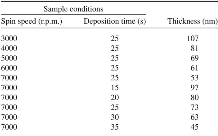
Table 1. Preparation conditions of PbI2 thin films and their
thicknesses.
Sample conditions
Spin speed (r.p.m.) Deposition time (s) Thickness (nm)
3000 25 107
4000 25 81
5000 25 69
6000 25 61
7000 25 53
7000 15 97
7000 20 80
7000 25 73
7000 30 63
7000 35 45
Optical properties were measured using optical transmittance and reflectance spectra recorded by a UV–Vis spectropho-tometer (Shimadzu UV-1800) in the 350–600 wavelength range. Electrical measurements were performed by a picoam-meter/voltage source (Keithley 6487) using two planar sil-ver (SPI supplies) printed electrodes of 5 mm in length separated by 5 mm.
3. Results and discussion
3.1 Thickness measurements
Table 1 summarizes deposition conditions of samples and their thickness. Thickness of the PbI2thin films, in all the
sam-ples, was around of 50–100 nm. From the table, the thickness of the thin films decreased as the deposition time and spin speed increased, a typical nature of spin-coated thin films. According to spin coating theory [12], during spinning due to the centrifugal force most of the PbI2solution is ejected from
the substrate leaving a thin liquid film of uniform thickness. When the solvent, (dimethylformamide) evaporates from this film, the PbI2deposits onto the substrate; the final thickness
is achieved by the complete evaporation of the solvent [13]. Both the radial liquid flow and the solvent evaporation rate increase with increase in speed, which in turn decrease the thin film thickness, as observed in the table.
Figure 1. X-ray diffraction patterns of PbI2 thin films deposited by varying the spin speed. The standard pattern of hexagonal PbI2
3.2 X-ray diffraction analysis
X-ray diffraction patterns of the thin films formed by vary-ing the spin speed are given in figure 1. In all the pat-terns, the peaks present at 2θ =12.73◦, 38.66◦ and 52.35◦ were assigned to the diffraction planes (001), (101), (002) and (003), respectively, of the hexagonal crystal structure [14] (PDF 07-0235). In all the cases, crystallite size was calculated using the Scherrer equation [15]:
D= 0.9λ
βcosθ, (1)
where λ is the wavelength of the X-ray beam,β the full-width at half maximum andθthe Bragg’s angle. The values were in the range of 16–23 nm, as shown in the figure.
In figure2, X-ray diffraction patterns of the films depo-sited for various durations are given. Similar to the thin films formed at various spin speed, all the diffraction peaks were identified as reflections from (001), (110), (202) planes of hexagonal crystal structure (PDF 07-0235), as noted in the
Figure 2. X-ray diffraction patterns of PbI2thin films deposited by varying the deposition time. The standard pattern of hexagonal PbI2(PDF 07-0235) is also included. Crystallite size calculated using
the Scherrer equation for each case is noted in the respective pattern.
figure. In this case, the peaks show a slight shift in the Bragg angles with respect to the standard pattern. This effect can be attributed to the presence of solvent molecules in the thin films. PbI2is composed of stacking layers of lead and iodine
atoms, traces of dimethylformamide molecules may be ac-commodated in between these layers. The crystallite sizes were in the range of 12–17 nm for the PbI2 thin films
de-posited for different durations at a spin speed of 7000 r.p.m., as noted in the figure. These XRD results showed that in ge-neral the thin film growth was oriented along [001] direction irrespective of the spin parameters. Formation of such highly oriented crystalline PbI2thin films may be because of the use
of dimethylformamide, a less soluble, polar solvent contain-ing electronegative oxygen atoms. Typically, the dissolution of inorganic PbI2 in an organic solvent depends on the
co-ordination between Pb2+ and electronegative oxygen atom
in the solvent molecules showing its solubility in different extents, depending on the solvent type. The commonly used solvents are dimethylformamide, dimethylacetamide, dime-thylsulphoxide andγ-butyrolactone. Among them, the slow-est crystallization of PbI2may be in dimethylsulphoxide due
to its largest solubility resulting from the strongest coordi-nation of sulphoxide oxygen with Pb2+ [16]. In a previous
report on the formation of lead perovskite thin films using spincoated PbI2precursor thin films, the role of solvents was
discussed [16]. In the report, a comparative study was done on spuncoated PbI2 thin films formed using
dimethylfor-mamide and dimethylsulphoxide as solvents. The thin films formed using dimethylsulphoxide exhibited an amorphous character, whereas highly crystalline thin films were obtained
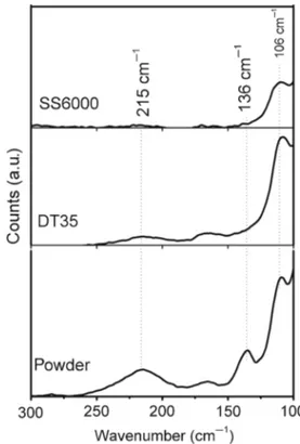
Figure 3. Raman spectra of the PbI2thin films (samples SS6000,
in the case of dimethylformamide. In our experiments using dimethylformamide as solvent, hexagonal-structured PbI2
thin films oriented along [100] direction were grown
3.3 Raman spectroscopy
In figure 3, the Raman spectra for the typical samples SS6000, DT35 and PbI2powder are shown. In all the spectra
three peaks are present at wavenumbers 96, 136 and 215 cm−1
as marked in the figure. All the peaks were identified as that originated from vibrational modes of PbI2 comparing with
the reported Raman peaks for this compound [17]. As men-tioned earlier, PbI2exists in different polytypes in which the
common form is 2H8 Each plane of I and Pb atoms is an identical series of triangles or overlapping hexagons. The unit cell of 2H contains three atoms. There are nine normal modes of vibration for the PbI2 2H polytype, which can be
represented in the irreducible D3d point group: = Alg+
Eg+2A2u+ 2Eu, where Eu and Eg are doubly degenerate.
There are three branches of acoustic modes and six branches of optical modes. The band at 96 cm−1 corresponds to the
Alg mode, and that at 136 cm−1 may be due to the resonant
optical excitation of the PbI2 molecules. The broadband at
215 cm−1was also reported as a characteristic peak of PbI 2
[17]. The well-defined principal band at 96 cm−1 for both the thin film samples implies their good crystalline nature in correlation with the well-defined XRD peaks. The intensity difference of the band may be due to the difference in their
thickness: SS6000 (low-intensity peak—thickness 61 nm) and DT35 (high-intensity peak—thickness 73 nm).
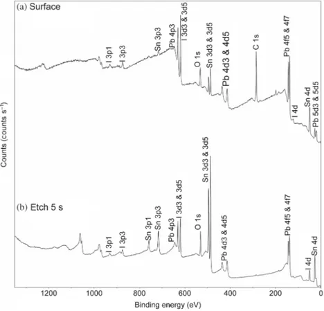
3.4 Composition
The chemical composition of the thin films was determined using the XPS analysis. Figure 4 shows the XPS survey spectra recorded before and after etching of the thin films deposited on FTO-coated glass substrates. In this case, the thin films were deposited on conductive substrates to avoid the surface charging effect. In the survey pattern, signals cor-responding to C, Pb, I and O are present, as marked in the figure. C1s signal was due to the adventitious carbon from the sample surface, which disappeared after Ar ion etching using argon ion of 2000 eV energy for 5 s. The presence of oxygen signal was from the substrates.
Figure5shows the high-resolution core level spectra for Pb 4f and I 3d peaks. The peaks were de-convoluted using Shirley-type background calculation and peak fitting using Gaussian-Lorentzian sum function, as shown in the figure. The black line represents the experimental data, and the red line shows the fitted curve. Fitting was done by keeping the separation energy (E)and the intensity ratio of Pb 4f dou-blet peaks at 4.87 eV and 3:4, respectively, as shown in the figure. The peak binding energy values of Pb 4f7/2and 4f5/2
core levels were 138.37 and 143.24 eV, in agreement with the respective values for PbI2 reported elsewhere [18]. The
peak binding energy values of I 3d5/2and 3d3/2 core levels
Figure 4. Survey spectra of a typical PbI2thin film: (a) sample surface and (b) after
were 619.5 and 630.98 eV, respectively, with the doublet sep-aration of 11.5 eV. These values are also in agreement with the values reported for PbI2in the literature [19]. The
oxida-tion state for lead was+4, meanwhile the oxidation state for iodine was−2. Further, from the figure Pb 4f doublet (136.5, 141.57 eV) shows the presence of a Pb0, which may be orig-inated due to the modification of sample’s surface chemistry by argon ion bombardments [20].
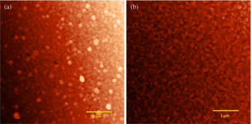
3.5 Morphology
Figure 6 shows AFM images of DT35 and SS6000 sam-ples recorded in semi-contact mode. As shown in figure6a, the surface morphology of DT35 consists of small grains, with an estimated roughness of 49 nm. Sample SS6000 (figure 6b) shows a similar morphology with larger grains with an average roughness of 8.7 nm. The difference in morphology might be attributed to the different deposition
conditions for the thin films, such as spin speed and duration of deposition. For the thin films formed with higher spin speed tends to decrease the roughness, whereas increase in the deposition time leads to form more solid particle to make the morphology rougher. Such parameters may be varied to form good quality thin films.
3.6 Optical properties
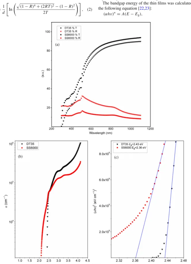
The optical transmittance and reflectance of the thin films by varying the deposition time and spin speed (DT35 and SS6000) in the wavelength range of 350–650 nm are shown in figure 7a. These thin films exhibited high transmittance in the visible spectrum, as high as 70% transmittance. The thin films were uniform and specularly reflective. Both sam-ples showed an absorption onset around 520 nm.
Figure7b and c shows the absorption coefficient of both samples and the respective Tauc plots to calculate the bandgap
Figure 5. Core level photoelectron spectra for Pb 4f and I 3d.
of the films. The absorption coefficient was calculated using the following equation [21]:
α= 1 d
In
(1−R)4+(2RT )2−(1−R)2
2T
, (2)
whereRis the optical reflectance,T the optical transmittance anddthe thickness of the thin film. The samples showed very high absorption coefficients, as high as 105cm−1.
The bandgap energy of the thin films was calculated from the following equation [22,23]:
(αhv)n=A(E−Eg), (3)
Figure 7. (a) Transmittance and reflectance spectra of the PbI2 films DT35 (7000 r.p.m. 35 s) and SS6000
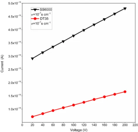
Figure 8. I–V curves of the PbI2films (samples SS6000 and DT35). The calculated
conductivities are shown in the order of 10−7S cm−1.
where Eg is the optical bandgap, and n = 2, 1/2 and 2/3,
respectively, for allowed direct, allowed indirect and forbid-den direct transitions, α the absorption coefficient at fre-quencyνand constantA. In all the thin films, the best fit was obtained forn =2, corresponding to direct allowed transi-tion. From the plot of(αhν)2vs.E, the Tauc plot, a straight
line is extrapolated to E-axis giving the value of Eg. The bandgap values were 2.43 and 2.36 eV for samples DT35 and SS6000, respectively. The bandgap values decreased as thickness increased, since sample SS6000 thickness was higher than that of sample DT35. These results are in good agreement with the earlier reports [24] on PbI2 thin films
deposited by different techniques.
3.7 Electrical properties
Figure 8 shows the I−V curve for samples SS6000 and DT35. From theI−V curves, a linear behaviour can be seen implying the ohmic nature of the silver contacts with the thin films. The resistivities and hence the conductivities of the thin films were calculated using the following equation:
ρ =Rbt
l , (4)
where R is the resistance of the sample,b the width of the electrodes, t the thickness of the sample and l the length of the electrodes. The conductivity of the material was
calculated by taking the inverse of the resistivity. Both samples exhibited conductivities of 10−7 S cm−1. Sample
SS6000 showed a higher conductivity than that of sam-ple DT35, which may be due to the larger crystalline size. These values of the conductivities are higher than those reported for lead iodide thin films deposited by solution methods [3].
4. Conclusions
Nanocrystalline thin films of lead iodide were obtained by spin coating. The thin films were uniform and polycrystalline with hexagonal structure as identified by XRD analysis, supported by the Raman spectra. The bandgap of the thin films was in the range of 2.3–2.4 eV. The thickness of the films decreased as spin speed increased. XPS measure-ments confirmed the elemental composition and chemical states of PbI2.
Acknowledgements
References
[1] Lee Y and Oh K 2012J. Instrum.7C0401
[2] Condeles J F and Martins T M 2004J. Non-Cryst. Solids338– 34081
[3] Ponpon J P U and Amann M 2001Thin Solid Films394277 [4] Novosad S S and Novosad I S 2002Inorg. Mater.381058 [5] Burschka J and Pellet N 2013Nature499316
[6] Condeles J F and Ando R A 2007J. Mater. Sci.43525 [7] Beckmann P A 2010Cryst. Res. Technol.45455
[8] Chaudhuri T K and Acharya H N 1982Mater. Res. Bull.17 279
[9] Mousa A M and Al-Rubaie N J 2009 Texture, Stress, and Microstructure2009Article ID 494537 1
[10] Bhavsar D S and Saraf K B 2003Mater. Chem. Phys.78630 [11] Condeles J F and Mulato M 2010J. Mater. Sci.461462 [12] Caldeira Filho A M and Mulato M 2011 Nucl. Instr. Meth.
Phys. Res. A63682
[13] Van Hardeveld R M and Wieldraaijer W 1995Appl. Surf. Sci. 84339
[14] Hall D B and Underhill P 1998 Polym. Eng. Sci. 38 2039
[15] Birkholz M 2006 Thin film analysis by X-ray scattering (Weinheim, Germany: Wiley-VCH Verlag GMBH and Co) [16] Wu Y, Islam A, Yang X, Qin C, Liu J, Zhang K, Peng W and
Han L 2014Energy Environ. Sci.72934
[17] Baibarac M, Smaranda I, Scocioreanu M, Mitran R A, Enculescu M, Galatanu M and Baltog I 2015Mater. Res. Bull. 70762
[18] Pederson L R 1982J. Electron Spect. Rel. Phen.28203 [19] Zheng Z and Wang S 2007J. Cryst. Growth308398 [20] Moulder J F, Stickle W F, Sobol P E and Bomben K D
1992Handbook of X-ray photoelectron spectroscopy (MN: Physical Electronics Division, Perkin Elmer Corp.)
[21] Fox M 2001Optical properties of solids(New York: Oxford University Press Inc.)
[22] Ahmad A and Saq’an S 2009Physica B4041 [23] Garza J G and Shaji S 2011Appl. Surf. Sci.25710834 [24] Shkir M and Abbas H 2012 J. Phys. Chem. Solids 73