Chemical bath deposition route for the synthesis of ultra-thin CuIn(S,Se)
2
based solar cells
S. Lugo
a, Y. Sánchez
b, M. Neuschitzer
b, H. Xie
b, C. Insignares-Cuello
b, V. Izquierdo-Roca
b,
Y. Peña
a, E. Saucedo
b,⁎
a
Universidad Autónoma de Nuevo León (UANL), Fac. de Ciencias Químicas, Av. Universidad S/N, Ciudad Universitaria, San Nicolás de Los Garza, Nuevo León C.P. 66451, Mexico
b
Catalonia Institute for Energy Research (IREC), Jardins de les Dones de Negre 1, 08930 Sant Adrià del Besòs, Barcelona, Spain
a b s t r a c t
a r t i c l e i n f o
Available online 15 October 2014
Keywords:
Copper indium sulfoselenide Indium sulfide
Copper sulfide Chemical bath deposition Raman spectroscopy Thinfilms Solar cells
CuIn(S,Se)2(CISSe) photovoltaic grade thinfilms are usually grown by expensive vacuum based methods or
chemical routes that require highly toxic precursors. In this work, we present the synthesis of CISSe absorbers by a simple chemical bath deposition (CBD) route. In thefirst step, In2S3/Cu2−xS stack was deposited as a
precursor by CBD on Mo-coated soda lime glass substrates, using respectively thioacetamide andN,N′ -dimethylthiourea as S source. Then the CISSe thinfilms were synthesized by the precursor's selenization at 450 °C. The obtainedfilms were characterized by X-ray diffraction (XRD), Raman spectroscopy and scanning electron microscopy (SEM). The tetragonal chalcopyrite structure of CISSe was identified by XRD and Raman, confirming that the major part of S was replaced by Se. SEM images show a compact and homogeneousfilm and by cross-section the thickness was estimated to be around 700 nm. Solar cells prepared with these absorbers exhibit an open circuit voltage of 369 mV, a short circuit current density of 13.7 mA/cm2, a
fill factor of 45% and an efficiency of 2.3%.
© 2014 Elsevier B.V. All rights reserved.
1. Introduction
I–III–VI group compounds are among the leading light-absorbing
semiconductors for thinfilm solar cells, with record efficiencies
exceed-ing 20% at laboratory scale and 15% at module scale[1]. Among them,
copper indium sulfur-selenide (CuIn(S,Se)2—CISSe) has been one of
the most promising photovoltaic materials because of its optical and electrical properties. It has a direct band gap between 1.0 and 1.5 eV
de-pending on S/Se ratio and an absorption coefficient exceeding 105cm−1
in the terrestrial solar spectrum range, which are ideal for the
fabrica-tion of thinfilm photovoltaic devices[2–4]. Although the band gap of
this material is not in the optimal range defined by the Shockley–
Queisser limit, CISe is a very interesting material for applications that
require high currents or as bottom cell in tandem concepts[5].
CISe thinfilms have been deposited by several techniques including
electrodeposition[6], electron beam evaporation[7], sputtering[8], and
chemical bath deposition (CBD)[4,9]. Efficiencies between 9 and 11%
have been reported using chemical based methods like particulate printing
processes, electrodeposition or hydrazine based methods[10].
Neverthe-less, these processes involve both toxic and hazardous precursors and/or complex synthesis methodologies. On the contrary, CBD is a simple and low cost method that produces uniform, adherent, and reproducible large
area thinfilms, and has been spotlighted as an alternative to these methods,
due to their potential to realize low cost PV devices[11].
Few studies reported solar cells using the CBD technique.
Vidyadharan et al.[12]first reported the synthesis of CuInSe2and its
in-corporation in a cell by the CBD technique on a single deposit, obtaining
a device with a maximum efficiency of 3.1%. Additionally, K. C. Rathod
et al.[13] deposited CuInSe2 layers by CBD, incorporating it in a
photoelectrochemical cell, obtaining an efficiency of 0.82%.
In this study, we present a different approach for the synthesis of
se-lenium rich CISSefilms by depositing In2S3/Cu2−xS stacked layers by
CBD on SLG/Mo substrates, followed by a reactive annealing under Se atmosphere. The advantage of the multi-stack precursor is that it allows for an accurate control of the cationic composition of CISSe by simply
varying the In2S3and Cu2−xS thicknesses. Using this approach a solar
cell with 2.3% maximum efficiency is reported, encouraging the future
development of this very low cost technology.
2. Experimental section
CISSe layers were synthesized using a two stage process: deposition
of In2S3/Cu2−xS stacked layers with a further annealing under Se
atmo-sphere in a graphite box. In thefirst step, the deposition of the indium
sulfide thinfilms was carried out on Mo-coated soda lime glass (SLG)
substrates (800 nm in thicknesses, 0.16Ω/□). The composition of the
chemical bath solution is: In(NO3)3(99.9%, Aldrich) 0.1 M, CH3COOH
0.5 M and CH3CSNH2(99%, Aldrich) 1 M at a pH of 2.0 that was adjusted
by adding diluted HCl; thefinal volume was adjusted to 100 mL with
de-ionized water (18 MΩ). The chemical reaction was carried out at 55 °C
⁎ Corresponding author.
E-mail address:[email protected](E. Saucedo).
http://dx.doi.org/10.1016/j.tsf.2014.10.039
0040-6090/© 2014 Elsevier B.V. All rights reserved.
Contents lists available atScienceDirect
Thin Solid Films
for 3 h and 45 min under continuous stirring, resulting in a layer with
380 nm in thickness. Then, during the second step Cu2−xS layers
were deposited on the In2S3/Mo/SLG substrate. The procedure given in
Ref.[14]was followed to deposit copper sulfide thinfilms by using
CuCl2·2H2O (99%, Aldrich) 0.5 M, Na2S2O3(98%, Aldrich) 1 M, and
N,N′-dimethylthiourea (99%, Aldrich) 0.5 M, with afinal volume of
100 mL. These chemical reagents are typically used in CBD processes for the growth of different materials, and although some of them contain organic molecules, C contamination is not expected. The chemical reaction was carried out at 70 °C for 1 h and 35 min under
continuous stirring, resulting in afilm of 250 nm in thickness. The selected
thicknesses correspond to Cu-rich conditions, in particular to a Cu/In ratio equal to 1.24. Cu-rich condition was selected because it promotes grain growth during the selenization process, although other compositions (in particular stoichiometric or Cu-poor) could be interesting for the optimization of the solar cell performance.
Finally, the CISSe thinfilms were synthesized by the selenization of
the In2S3/Cu2−xS stack precursors in a tubular furnace, using a graphite
box with a volume of 23.5 cm3, containing 20 mg of Se powder with a
total pressure of 1 bar under Ar atmosphere. The system was heated at 20 °C/min up to 450 °C for 30 min, and then naturally cooled down. The total process takes approximately 120 min.
The structural properties of the obtainedfilms were analyzed by
X-ray diffraction (XRD) using an X-X-ray diffractometer Siemens D-500 in
θ–2θconfiguration (Cu Kαradiation,λ= 1.5418 Å). The surface
mor-phology andfilm grain size were analyzed by scanning electron
micros-copy (SEM, FEI NovaTM NanoSEM 230) using a work distance of 5 mm
and an operating voltage of 5 kV. The thinfilms obtained were also
char-acterized by Raman spectroscopy in backscattering configuration using
a Raman probe developed at the Catalonia Institute for Energy Research,
coupled with an opticalfiber to an iHR320 Horiba Jovin Yvon
spectrom-eter. In order to optimize the signal of the secondary phases present in the layer, the Raman characterization has been performed under 532 nm and 785 nm excitation wavelengths. In both excitation wave-lengths the optimal excitation power density has been studied in order to avoid the thermal effect in the measurements. All
measure-ments have been calibratedfixing the 520 cm−1Raman shift for the
main mode of the Si monocrystal spectrum.
For the solar cells, absorbers were etched with a KCN solution (5% w/V, 2 min), CdS buffer layer (~60 nm) was deposited by CBD, and intrinsic
ZnO and ZnO:Alfilms were grown by pulsed direct current magnetron
sputtering deposition (CT100 Alliance Concepts). For the optoelectronic
characterization, 3 × 3 mm2cells were scribed using a micro-diamond
scriber (MR200 OEG). Measurement of the optoelectronic properties was carried out using a pre-calibrated Sun 3000 Class AAA solar simulator
from Abet Technologies (uniform illumination area of 15 × 15 cm2, AM
1.5filter) and the external quantum efficiency (EQE) of the devices was
also measured, using a Bentham PVE300 system.
3. Results and discussion
XRD diffractograms are shown inFig. 1, including the as deposited
In2S3/Cu2 −xS layers (a) and the as annealed CISe layer (b). The
diffractogram of the as deposited In2S3/Cu2−xS precursor layer is
dom-inated for the diffraction peaks corresponding to Mo (JCPDSfile
042-1120). Additionally, broad and weak peaks at 28.4°, 33.6° and 48.2°, and a shoulder at 29.4° can be observed. These contributions are
assigned to In2S3[15]and Cu2−xS (JCPDSfile 29-6578) phases. The
weak intensity of these peaks and their high full width at half maximum (FWHM) indicate the amorphous nature of the precursors. After the
selenization of the In2S3/Cu2−xS precursors, the crystal structure of
the resulting polycrystalline CISSe thinfilms correspond to the
tetrago-nal chalcopyrite phase (JCPDS 040-1487), with a [S]/([S] + [Se]) ratio of
0.08, estimated by the Vegard's law[16]. This suggests that during the
annealing process, almost all the S was substituted by Se, leading to a Se rich CISSe chalcopyrite phase. The symmetry of the CISSe diffraction
peaks and their low FWHM (FWHM = 0.26° from (112) at 24.75°) sug-gest a high crystalline quality absorber and constant CISSe in depth composition. Additionally, a weak contributions at 29.0° and 42.0° and
a shoulder centered at 39.2° could be identified with diffraction peaks
corresponding to the Cu2−x(S,Se) alloy. The formation of this phase is
in agreement with the rich composition of the precursor. This
Cu-rich phase act as crystallizationflux, facilitating the grain growth and
allowing obtaining large grain layers[17]. Also, peaks at 31.7° and
56.0° are assigned to MoSe2(JCPDS 29-0914), demonstrating that Mo
was partially selenized during the annealing process. This confirms
that the methodology proposed in this paper is useful for the synthesis of Se rich CISSe chalcopyrite layers from the selenization of Cu and In
sulfide precursors deposited by CBD.
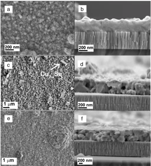
InFig. 2a the top view of Cu2 −xS layer is presented, where
nanometric scale needles are observed. The cross section view of the
stacked precursor (Fig. 2b) supports the amorphous like nature of the
bi-layer, presenting a veryfine grain structure. After selenization,
the morphology of the surface changes drastically (Fig. 2c to f). Larger
grains are observed in the surface (around 200 nm) confirming the
ad-equate crystallization of the material. Also, hexagonal platelets are
clearly seen on top (seeFig. 2c), which are typically associated with
Cu2−xSe and/or Cu2−xS, confirming the presence of Cu-rich secondary
phases. Using the cross sectional views of the absorber we can estimate
a thickness of 740 nm approximately (Fig. 2d), with a very thin MoSe2
layer (less than 50 nm), confirming the good crystallization of the
pre-cursor, and demonstrating the potentiality of this approach to produce
layers with large grain structure. After KCN etching (Fig. 2e and f for
top and cross sectional views respectively), the hexagonal platelets are effectively removed from the surface, supporting that these over-growths are Cu-chalcogenide binary phases. Additionally, the surface is clearly smooth when compared with the as annealed absorber,
being this etching effect beneficial for the hetero-junction properties.
InFig. 3the Raman spectra of the as grown In2S3(spectra a1 and b1),
In2S3/Cu2−xS stacked layers (spectra a2 and b2), and the corresponding
20
30
40
50
60
In
2S
3Cu
2-xS
2
θ
(°)
(Intensity)
0.
5
(arb. units)
Cu
2-x(S,Se)
Cu
2-x(S,Se)
CISSe
MoSe
2CISSe
CISSe
CISSe
CISSe
CISSe
Mo
CISSe
MoSe
2Cu
2-x(S,Se)
In
2S
3In
2S
3a
b
Fig. 1.XRD diffractograms: a) as-deposited In2S3/Cu2−xS multi-stack precursor, and
Fig. 2.SEM top (a) and cross sectional (b) views of the as-prepared precursors, top (c) and cross sectional (d) views of the as annealed one, and top (e) and cross sectional (f) views of the as etched layers using a KCN solution.
Fig. 3.Raman spectra of In2S3(a1–b1), In2S3/Cu2−xS (a2–b2) and CuIn(S,Se)2(a3–b3) under 532 nm and 785 nm excitation wavelengths. Also the reference spectra of OVC phase is
absorber after selenization (spectra a3 and b3), using 532 nm and 785 nm are presented. The penetration depth under both excitation wavelengths is estimated below 100 nm providing information from the sample surface. The a1 and b1 Raman spectra are characterized by
a broad band in the region of 150–400 cm−1. The detection of this
band confirms the formation of amorphous like In2S3[18]. Additionally
under a 785 nm excitation wavelength a small contribution identified
with elemental sulfur is observed[19]. The presence of this signal
sug-gests the precipitation of rather small quantities of sulfur during the
growth of In2S3. In the spectra corresponding to the In2S3/Cu2−xS
stack (a2 and b2) the broad band assigned to amorphous like In2S3is
clearly modified, with changes in the shape and ratios between the
dif-ferent contributions, suggestion and improvement of the crystalline
quality[18]. This crystallization could be associated with the high
tem-peratures used for the chemical bath deposition of Cu2−xS.
Additional-ly, a weak contribution at 473 cm−1identi
fied as Cu2−xS phase is
detected[20]. From the Raman analysis, there are no clear evidences
of the inter-mixing between Cu sulfide and In sulfide precursors, with
the concomitant formation of CuInS2or related phases. It is important
to remark that the In2S3Raman signal is also observed in the spectra
a2 and b2 because the upmost Cu2−xS layer is very porous (as is clearly
observed inFig. 2a), and is not enough to cover completely the In2S3
bottom layer.
After the selenization of this precursor, the Raman spectrum with
green excitation (a3) shows a main peak at 176 cm−1, with three
weak-er contributions at 212 cm−1, 228 cm−1and 290 cm−1. The low FWHM
of the main A1 mode (10 cm−1, in this system the FWHM of the
520 cm−1mode of crystalline Si used as reference is 6.4 cm−1) confirms
the high crystalline quality of the absorber. These contributions are
assigned to very Se-rich CuIn(S,Se)2chalcopyrite phase (with more
than 90% of Se)[21], in close agreement with the XRD analysis. Using
a 785 nm excitation wavelength, two additional features are observed
in the 390–475 cm−1frequency region, and are tentatively assigned
to sulfur rich Cu2−x(S,Se)[22,23]. The formation of this phase is in
agreement with the Cu-rich composition of the precursor. Additionally,
the intensity of the 228 cm−1mode increases (see spectrum b3) under
785 nm excitation. Under this condition, the increase of this contribu-tion is assigned to the presence of Ordered Vacancy Compound (OVC) phases, as is illustrated in the OVC reference spectra (corresponding to
CuIn3Se5) in the samefigure[24]. Differences between the reference
and the absorber spectra correspond to different OVC compositions
(OVC phases have several stoichiometries including CuIn5Se8,
CuIn2Se3.5, and CuIn1.5Se2)[24,25]. Although the OVC phases are usually
associated with Cu-poor conditions, it was reported that these phases
can be also formed close to Cu–Se secondary phases in Cu-rich layers,
as those observed inFig. 2a[17]. In this case, the grains in contact
with the Cu–Se binary phase can be Cu-poor (although the overall
com-position of the layer is Cu-rich), explaining the unexpected presence of OVC phases in Cu-rich layers.
To confirm the potential of the absorbers produced by the two stage
process, CISSe layers obtained from the selenization of In2S3/CuxS stacks
at 450 °C/30 min were tested as absorber materials in solar cells.Fig. 4a
shows the obtained current density–voltage (J–V) curve for the best cell,
where the following optoelectronic parameters were extracted: open
circuit voltage, Voc= 369 mV; short circuit current density, Jsc=
13.7 mA/cm2;fill factor, FF = 45%; and efficiency of 2.3%. The V
ocis
only slightly lower than those reported in literature for the best CISe
solar cells[10], suggesting that the absorber has a good quality, as was
demonstrated before using Raman spectroscopy. Also, the presence of
OVC's in the surface detected by this technique (seeFig. 3b) could
con-tribute to the reduction of the density of defects[25,26], enhancing the
cell's voltage. Nevertheless, the Jscand FF of the cell are remarkably
lower than values expected for this material[27,28]. The low current
could be related, at least in part, to the thinner absorber which is only
700 nm in thickness with respect to typical 1.5–2.0μm used in this
tech-nology. The low FF can be explained by the low shunt and high series
resistance characteristics of this device that could be related to the Cu-rich conditions employed in this work (and the concomitant formation
of Cu–Se binary phases). Additionally, no optimized junction and/or
electrical contacts could be the reason of these low values. Finally, the
voids observed inFig. 2b are also contributing to the deterioration of
the current of the cell. The external quantum efficiency (EQE %)
spec-trum for the CISSe thinfilm solar cell is shown inFig. 4b. The maximum
value of the EQE is around 40%, confirming the non-optimized charge
carrier collection, which origin is under study to improve the solar cell characteristics. Using the high wavelength region of the EQE we esti-mate a band gap of the esti-material equal to 1.0 eV, in agreement with XRD and Raman spectroscopy, where Se-rich CISSe absorber was
ob-served. Nevertheless, although the efficiency of the devices presented
here is considered low, the technique has potentiality to produce a pho-tovoltaic grade material. Future improvements in the cationic
composi-tion (Cu/In ratio), modifications in the bath conditions to increase the
deposition rate, optimization of the annealing parameters, passivation
of the rear contact, etc., will be a pre-requisite to increase the efficiency.
In summary, CISSe based thinfilm solar cells obtained in this work
by the CBD technique are viable for low cost concepts for the synthesis of ultra thin Se-rich CISSe absorbers. However, there are many aspects
to be considered in the future for increasing the efficiency of these
de-vices. An interesting alternative is to use a passivation layer formed by
MgF2/Al2O3, as was reported by B. Vermang et al.[28], to increase the
Vocand Jscand consequently the device efficiency.
4. Conclusions
CuIn(S,Se)2ultra-thinfilms were prepared on Mo/SLG, by means the
selenization of chemically deposited In2S3/Cu2−xS stacked layers. The
structural, morphological and optical properties of precursors as well as absorbers were investigated. XRD and Raman spectroscopy show
that the precursor is formed by amorphous like In2S3and Cu2−xS
bina-ry phases, with rather marginal mixing between them. After
selenization, Se-rich CuIn(S,Se)2layers with large grains, tetragonal
chalcopyrite structure and approximately 700 nm in thickness were
ob-tained, with Cu2−x(S,Se) binary compound as the secondary phase.
Solar cells prepared with this absorber exhibit a maximum conversion
efficiency of 2.3%, with 369 mV of Voc, 13.7 mA/cm2of Jscand 45% of
FF. In summary, the possibility to synthesize photovoltaic grade Se-rich CISSe absorbers by a two step CBD technique is demonstrated.
Acknowledgments
The research leading to these results has received funding from the People Program (Marie Curie Actions) of the European Union's Seventh
Framework Program FP7/2007–2013/ under REA grant agreement No.
316488 (KESTCELLS) and No. 285897 (INDUCIS), by European Regional Development Funds (ERDF, FEDER Programa Competitivitat de
Catalu-nya 2007–2013), and CONACyT project No. 178228 and Laboratory
Re-search and Technological Development 2009 No. 124177. Authors from IREC and IN2UB belong to the M-2E (Electronic Materials for Energy) Consolidated Research Group and the XaRMAE Network of Excellence
on Materials for Energy of the“Generalitat de Catalunya”. Y.S. thanks
the PTA fellowship (PTA2012-7852-A), H.X. the“China Scholarship
Council”fellowship (CSC No. 201206340113), V.I. the“Juan de la Cierva”
fellowship (JCI-2011-10782) and E.S. the“Ramon y Cajal”fellowship
(RYC-2011-09212).
References
[1] M.A. Green, K. Emery, Y. Hishikawa, W. Warta, E.D. Dunlop, Solar cell efficiency ta-bles (version 43), Prog. Photovolt. Res. Appl. 22 (2014) 1.
[2] H. Liu, Z. Jin, J. Wang, J. Ao, G. Li, Well-dispersed CuInSe2nanoplates and nanoplates-ink-coated thinfilms for photovoltaic application by a triethylene glycol based solu-tion process, Mater. Lett. 94 (2013) 1.
[3] C.R. Kim, S.Y. Han, C.H. Chang, T.J. Lee, S.O. Ryu, Synthesis and characterization of CuInSe2thinfilms for photovoltaic cells by a solution-based deposition method, Curr. Appl. Phys. 10 (2010) S383.
[4] P.P. Hankare, K.C. Rathod, P.A. Chate, A.V. Jadhav, I.S. Mulla, Preparation and charac-terization of CuInSe2thinfilms by chemical bath deposition technique, J. Alloys Compd. 500 (2010) 78.
[5] Z. Jehl-Li-Kao, T. Kobayashi, T. Nakada, CuIn(Se1−xTex)2solar cells with tunable narrow-bandgap for bottom cell application in multijunction photovoltaic devices, Energy Mater. Sol. Cells 119 (2013) 144.
[6] S. Hamrouni, M.S. AlKhalifah, M.F. Boujmil, K. Ben Saad, Preparation and character-ization of CuInSe2electrodeposited thinfilms annealed in vacuum, Appl. Surf. Sci. 292 (2014) 231.
[7] H. Abdullah, S. Habibi, Effect of annealing temperature on CuInSe2/ZnS thin-film solar cells fabricated by using electron beam evaporation, Int. J. Photoenergy 2013 (2013) 568904.
[8] M. Oertel, T. Hahn, H. Metzner, W. Witthuhn, CuInSe2solar cells by sequential ab-sorber layer processing, Phys. Status Solidi C 6 (2009) 1253.
[9] C.-H. Wu, J.-S. Ma, S.-H. Lin, C.-H. Lu, Synthesis of CuInSe2thinfilms onflexible Ti foils via the hydrothermally-assisted chemical bath deposition process at low tem-peratures, Sol. Energy Mater. Sol. Cells 112 (2013) 47.
[10]C.J. Hibberd, E. Chassaing, W. Liu, D.B. Mitzi, D. Lincot, A.N. Tiwari, Non-vacuum methods for formation of Cu(In, Ga)(Se, S)2thinfilm photovoltaic absorbers, Prog. Photovolt. Res. Appl. 18 (2010) 434.
[11] M.D. Mahanubhav, V.R. Patil, P.K. Khanna, Studies on chemically deposited CuInSe2 thinfilms, Mater. Lett. 61 (2007) 2058.
[12] P.K. Vidyadharan Pillai, K.P. Vijayakumar, Characterization of CuInSe2CdS thin-film solar cells prepared using CBD, Sol. Energy Mater. Sol. Cells 51 (1998) 47.
[13] K.C. Rathod, P.A. Chate, K.M. Garadkar, D.J. Sathe, I.S. Mulla, Chemical deposition of CuInSe2thinfilms by photoelectrochemical applications, J. Alloys Compd. 511 (2012) 50.
[14] M.T.S. Nair, Laura Guerrero, P.K. Nair, Conversion of chemically deposited CuS thinfilms to Cu1.8S and Cu1.96S by annealing, Semicond. Sci. Technol. 13 (1998) 1164.
[15] P. Pistor, R. Caballero, D. Hariskos, V. Izquierdo-Roca, R. Wa, S. Schorr, R. Klenk, Quality and stability of compound indium sulphide as source material for buff-er laybuff-ers in Cu(In, Ga)Se2solar cells, Sol. Energy Mater. Sol. Cells 93 (2009) 148.
[16] A.R. Denton, N.W. Ashcroft, Vegard's law, Phys. Rev. A 43-6 (1991) 3161.
[17]E. Saucedo, V. Izquierdo-Roca, C.M. Ruiz, L. Parissi, C. Broussillou, P.-P. Grand, J.S. Jaime-Ferrer, A. Pérez-Rodríguez, J.R. Morante, V. Bermúdez, Key role of Cu–Se bina-ry phases in electrodeposited CuInSe2precursors onfinal distribution of Cu–S phases in CuIn(S,Se)2absorbers, Thin Solid Films 517 (2009) 2268.
[18]B. Asenjo, C. Guillén, A.M. Chaparro, E. Saucedo, V. Bermudez, D. Lincot, J. Herrero, M.T. Gutiérrez, Properties of In2S3thinfilms deposited on ITO/glass substrates by chemical bath deposition, J. Phys. Chem. Solids 71 (2010) 1629.
[19] A.T. Ward, Raman spectroscopy of sulfur, sulfur–selenium, and sulfur–arsenic mix-tures, J. Phys. Chem. 72 (1968) 4133.
[20]P. Kumar, M. Gusain, R. Nagarajan, Synthesis of Cu1.8S and CuS from copper– thio-urea containing precursors; anionic (Cl−, NO3−, SO42−) influence on the product stoi-chiometry, Inorg. Chem. 50 (2011) 3065.
[21] V. Izquierdo-Roca, X. Fontané, J. A̧lvarez-Garcı́a, L. Calvo-Barrio, A. Pérez-Rodríguez, J.R. Morante, C.M. Ruiz, E. Saucedo, V. Bermúdez, Electrochemical synthesis of CuIn(S,Se)2alloys with graded composition for high efficiency solar cells, Appl. Phys. Lett. 94 (2009) 061915.
[22] I. Motohiko, K. Shibata, H. Nozaki, Anion distributions and phase transitions in CuS1−xSex(x= 0–1) studied by Raman spectroscopy, J. Solid State Chem. 105 (1993) 504.
[23] V. Izquierdo-Roca, A. Pérez-Rodríguez, A. Romano-Rodríguez, J.R. Morante, J. A̧lvarez-Garcı́a, L. Calvo-Barrio, V. Bermudez, P.P. Grand, O. Ramdani, L. Parissi, O. Kerrec, Raman microprobe characterization of electrodeposited S-rich CuIn(S,Se)2 for photovoltaic applications: microstructural analysis, J. Appl. Phys. 101 (2007) 103517.
[24] C.-M. Xu, X.-L. Xu, J. Xu, X.-J. Yang, J. Zuo, N. Kong, W.-H. Huang, H.-T. Liu, Composi-tion dependence of the Raman A1mode and additional mode in tetragonal Cu–In– Se thinfilms, Semicond. Sci. Technol. 19 (2004) 1201.
[25] C. Insignares-Cuello, C. Broussillou, V. Bermúdez, E. Saucedo, A. Pérez-Rodríguez, V. Izquierdo-Roca, Raman scattering analysis of electrodeposited Cu(In, Ga)Se2solar cells: impact of ordered vacancy compounds on cell efficiency, Appl. Phys. Lett. 105 (2014) 021905;
C.M. Ruiz, X. Fontané, A. Fairbrother, V. Izquierdo-Roca, C. Broussillou, S. Bodnar, A. Pérez-Rodríguez, V. Bermúdez, Impact of electronic defects on the Raman spectra from electrodeposited Cu(In,Ga)Se2solar cells: application for non-destructive de-fect assessment, Appl. Phys. Lett. 102 (2013) 091106.
[26]S. Siebentritt, L. Gütay, D. Regesch, Y. Aida, V. Deprédurand, Why do we make Cu(In, Ga)Se2solar cells non-stoichiometric? Sol. Energy Mater. Sol. Cells 119 (2013) 18.
[27] J. Song, S.S. Li, C.H. Huang, O.D. Crisalle, T.J. Anderson, Device modeling and simula-tion of the performance of Cu(In1−x, Gax)Se2solar cells, Solid State Electron. 48 (2004) 73.
[28] Bart Vermang, Jörn Timo Wätjen, Viktor Fjällström, Fredrik Rostvall, Marika Edoff, Ratan Kotipalli, Frederic Henry, Denis Flandre, Employing Si solar cell technology to increase efficiency of ultra-thin Cu(In,Ga)Se2solar cells, Prog. Photovolt. Res.