Novel InN/InGaN multiple quantum well structures for slow‐light generation at telecommunication wavelengths
5
0
0
Texto completo
(2) Novel InN/InGaN Multiple Quantum Well structures for Slowlight generation at telecommunication wavelenghts a),1. 2. 1. 2. 2. F. B. Naranjo , P. K. Kandaswamy , S. Valdueza-Felip , L. Lahourcade , V. Calvo , M. González1 3 3 2 Herráez , S. Martín-López , P. Corredera , and E. Monroy 1. Grupo de Ingeniería Fotónica, Departamento de Electrónica, Escuela Politécnica Superior, Universidad de Alcalá Campus Universitario, 28871 Alcalá de Henares, Madrid, Spain. 2 CEA-Grenoble, INAC / SP2M, 17 rue des Martyrs, 38054 Grenoble cedex 9, France. 3 Departamento de Metrología, Instituto de Física Aplicada, (CSIC), 28006 Madrid, Spain. Received ZZZ, revised ZZZ, accepted ZZZ Published online ZZZ (Dates will be provided by the publisher.) PACS 71.55.Eq, 78.20.Ci, 25.20.Dc, 77.65.Ly, 81.10.-h Corresponding author: e-mail [email protected], Phone: +00 34 91 885 6658x5, Fax: +00 34 91 885 6591. The third order susceptibility is responsible for a variety of optical non-linear phenomena -like self focusing, phase conjugation and four-wave mixing- with applications in coherent control of optical communication. InN is particularly attractive due to its near-IR bandgap and predicted high nonlinear effects. Moreover, the synthesis of InN nanostructures makes possible to taylor the absorption edge in the telecomunication spectral range and enhance nonlinear parameters thanks to carrier confinement. In this work, we assess the nonlinear optical behavior of InN/InxGa(1-x)N (0.9>x>0.7) multiple-quantum-well (MQW) structures grown by plasma-assisted MBE on GaN-on-sapphire. 1 Introduction. Nowadays, optical telecommunications networks require optical-to-electrical conversion at each node. In order to fully exploit the bandwidth of the optical fibre, the next generation of photonic systems for optical telecommunications should evolve to an alloptical approach. All-optical signal processing requires new optical devices for ultrafast pulse generation, dispersion and delay control (“slow light generation”), switching, reamplification and wavelength conversion. These new generation devices should be characterized by low optical control power and high speed operation, thus the use of resonant nonlinearities appears as a feasible approach for these devices [1]. Novel low-dimensional semiconductor structures can attain the required specifications, taking advantage of properties like high third order non-linear optical susceptibility and possibility of band-gap engineering to tune the wavelength operation. “Slow light generation” refers to the possibility of controlling the speed of the light in an optical medium. Slow light devices should make possible the fabrication of optically controlled delay lines for their application to. templates. Low-temperature (5 K) photoluminescence measurements show near-IR emission whose intensity increases with the In content in the barriers, which is explained in terms of the existence of piezoelectric fields in the structures. The nonlinear optical absorption coefficient, 2, were measured at 1.55 µm using the Z-scan method. We observe a strong dependence of the nonlinear absorption coefficient on the In content in the barriers. Saturable absorption is observed for the sample with x = 0.9, with 2 ~ -9x103 cm/GW. For this sample, an optically controlled reduction of the speed of light by a factor S ~ 80 is obtained at 1.55 µm.. all-optical routers in packet-switched networks. In general, the control of optical information by delay introduction has been done by using optical-fiber delay lines (i.e. optical fiber closed loops) and/or structures based on waveguide-dispersion. These procedures show some limitations, since it is not possible to choose any delay time and they require a narrow bandwidth, respectively [2][3]. In case of an optical controlled variable delay line, a laser beam should control the speed of light travelling through the active material. This optical control requires that the active material presents a high nonlinear response, including saturable absorption (SA) and long carrier recovery times. Previous work shows that InN has recovery time in the range of ps [4], presents saturable absorption and close to resonant behaviour at the telecommunication wavelength of 1.55 µm [5]. On the other hand, considering the usual properties of low dimensional structures, it is expected that the multiple quantum well (MQW) based on InN should show higher recovery times, and enhanced nonlinear behaviour, including the possibility of tuning.
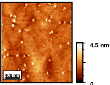
(3) the resonance wavelength anywhere in the optical fiber transparency band [3]. In this sense, the aim of the present work is to study the feasibility of InN-based QW for applications in all optical-based devices operating at 1.55 µm 2 Experimental details In this work, we have studied a set of novel InN/InGaN MQW structures developed for resonance at 1.55 µm wavelength. The structures were grown by molecular beam epitaxy on GaN template substrates, and they consist of 41 periods of InN well and InxGa(1-x)N barrier with In content ranging from x ~ 0.7 to x ~ 0.9. The nominal well and barrier thicknesses are 4.5 nm and 7 nm, respectively. Regarding the growth conditions, the whole structure is grown at the same growth temperature, 450ºC. The first layer of the structure was InN, in order to relax the lattice mismatch between the substrate and the heterostructure. Finally, a 1 µm-thick InN layer was grown to be used as reference. The surface morphology was analysed by atomic force microscopy. Regarding the linear optical properties of the samples, they have been obtained through low temperature (5K) photoluminescence (LT-PL) measurements using an Ar (514 nm) laser as excitation source. Z-Scan method was used to estimate the non-linear absorption coefficient of the samples. This method is based on measuring the differential transmittance of the sample when changing the input power density. This is performed by moving the sample forward the optical axis of a focussed Gaussian beam (Z axis direction). During the measurement, the transmittance of the sample is recorded with the Z position. If it increases with the power density, the sample presents SA. On the contrary, if it decreases with the power density, the sample presents reverse saturable absorption (RSA) [6]. Z-Scan measurements were carried out using a femto fiber laser source with 100 MHz of repetition rate and 100 ps of pulse width. The obtained experimental results were fit to the expression (1) in order to obtain the non linear absorption coefficient, 2.. Top ( z ) 1 where. I0. is. 1 2 I 0 Leff 2 2 1 z z0. (1). maximum input power, Leff (1 e ) is the effective length of the sample, and z0 is the Rayleight range of the laser beam. z. the. 3 Results and discussion The analysed InN/InxGa(1-x)N MQW structures show a surface roughness (rms) measured in 2 x 2 µm2 areas. below 2 nm for all cases. Form these results, a good well-barrier interface quality is expected, as the structures does not have any cap layer. On the other hand, it is worth mentioning that the lattice mismatch between well and barrier for the sample with 70 % of barrier In content is as high as 3 %, being even higher than the estimated one in AlN/GaN heterostructures, of 2.5 % [7].. 4.5 nm. 400 nm. 0 2. Figure 1. AFM image of 2 x 2 µm area for the InN/InxGa(1x)N MQW sample with x = 0.9. This sample shows an rms of 0.5 nm.. Figure 2 shows the normalized LT-PL spectra of the InN/InxGa(1-x)N MQW samples with x ~ 0.8 and x ~ 0.9 In content in the barrier, and the bulk InN layer. IR emission is observed for the InN reference sample, with an emission energy of 0.73 eV and a full width at half maximum (FWHM) of 0.60 meV. The IR emission is enhanced in the MQW sample with x ~ 0.9, which shows an emission centred at 0.72 eV, with a FWHM as low as 44 meV. As it can be observed, the PL emission energy suffers a redshift and a decrease of intensity when decreasing the In content in the barrier. Thus, in case of sample with x ~ 0.8 the emission energy of the IR peak is 0.67 eV with a FWHM of 70 meV. Finally, no PL emission was detected for the sample with the lowest In content in the barrier, 70 %. This behaviour is attributed to the existence of high piezoelectric fields in the structures [8]. 3. 5K. Normalized PL intensity. 1 2 3 4 5 6 7 8 9 10 11 12 13 14 15 16 17 18 19 20 21 22 23 24 25 26 27 28 29 30 31 32 33 34 35 36 37 38 39 40 41 42 43 44 45 46 47 48 49 50 51 52 53 54 55 56 57. 1 m InN. 2. InN / In0.9Ga0.1N. 1. InN / In0.8Ga0.2N. 0. 0.60. 0.65. 0.70. 0.75. 0.80. 0.85. 0.90. Energy (eV). Figure 2. Normalized Low Temperature (5 K) PL spectra of the analysed InN/InxGa(1-x)N MQW samples together with an InN reference layer. No PL emission has been observed from sample with x ~ 0.7..
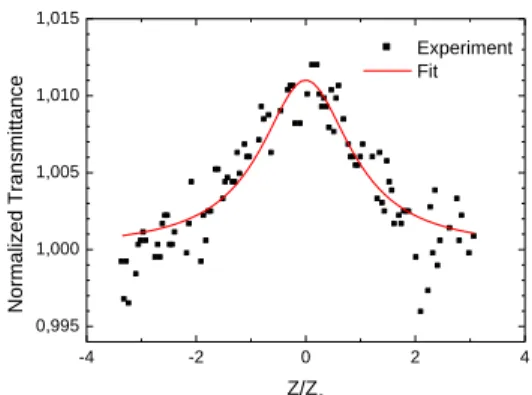
(4) EG(InN),LT = 0.73 eV. 0.75 InN. 0.70. 0.65. PL peak E1-H1 Strained E1-H1 Relaxed. 1.00. 0.95. 0.90. 0.85. 0.80. 0.75. Experiment Fit 1,010. 1,005. 1,000. 0,995 -4. -2. 0. 2. Figure 4. Z-Scan measurements on InN films layers.. The Z-Scan measurements show different properties in the MQW samples depending on the In content in the barrier. For the sample with x ~ 0.9 (figure 5), we have observed SA with a value of 2 = -9150 cm/GW. The increase of this coefficient compared to bulk InN is attributed to quantization effects. It is expected from simulations of the electronic structure that in this sample the optical excitation takes place from H1 to the continuum in the conduction band, since the excitation energy ~0.79 eV (1.55 µm) is higher than the E1-H1 recombination energy.. 0.70. In content. Figure 3. Estimated E1-H1 recombination energy for the analysed samples obtained considering the structure fully relaxed (down triangles) and fully strained (squares).. The non-linear absorption coefficient of the samples was estimated using Z-Scan measurements. All the measurements were carried out at power levels below 0.8 GW/cm2, which is the minimum power for obtaining a measurable response from the substrate. Figure 4 shows a Z-Scan measurement performed on the reference InN sample. It reveals SA behaviour with 2 = -1450 cm/GW, it being the first measurement of this coefficient on InN at 1.55 µm. The SA effect is attributed to band filling of the states, as it has been observed by other authors [5]. The high value obtained for 2 is related to the resonant conditions of the excitation in the measurements.. 4. Z/Z0. Experiment Fit. 1.004. Normalized Transmittance. 0.80. 1,015. Normalized Transmittance. The band structure of the InN/InGaN MQW was calculated from 1D self-consistent simulations using Nextnano3 software [9]. From these simulations the expected recombination energy between the first confined level in the well for electrons and holes (E1-H1) was calculated. Figure 3 shows the simulation results considering both the MQW fully relaxed and fully strained on InN. As it can be observed, the dependence of PL emission energy on the In content in the barrier follows the tendency of the expected E1-H1 recombination energy considering the QWs fully strained. At the same time, the electrical simulation of the sample with x ~ 0.7 predicts a huge piezoelectric field in the structure (4.9 MV / cm). This high internal electric field hinders radiative recombination due to the separation of confined electron and holes.. Energy (eV). 1 2 3 4 5 6 7 8 9 10 11 12 13 14 15 16 17 18 19 20 21 22 23 24 25 26 27 28 29 30 31 32 33 34 35 36 37 38 39 40 41 42 43 44 45 46 47 48 49 50 51 52 53 54 55 56 57. 1.003 1.002 1.001 1.000 -4. -2. 0. 2. 4. Z/Z0. Figure 5. Z-Scan measurements of InN/In0.9Ga0.1N MQW.. The sample with x ~ 0.8 shows RSA, which is attributed to two-photon absorption from the H1 level. Finally, sample with x ~ 0.7 does not show any non-linear effect for input power below 0.8 GW/cm2. Taking into account the saturable absorption and the high 2 value obtained the sample with x ~ 0.9, we have studied its application to slow light generation. The slow-light generation is based on saturation of absorption, which creates a dip in the absorption spectra. This dip leads to an abrupt change in the refractive index with the wavelength and thus a change in the group index, or the speed of wave packet through the sample. This.
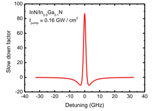
(5) process is the so-called Slow light generation. For the estimation of the reduction of the speed of light, or the slow-down factor (S-factor), we have considered a Lorentzian shape for the induced depth in the absorption [10], , following the equation (2). 2 I. 1 0 1 2 . (2). 2. where I and 0 are the pump intensity and the resonance frequency (200 THz for 1.55 µm). The FWHM bandwidth, is calculated as the inverse of the lifetime of the photogenerated carriers, [11]. Taking a value of ~ 400 ps, which is two order of magnitude higher that the obtained one for InN bulk layer under non-linear regime [12], we have estimated a slow down factor of 80. Figure 6 shows the calculated S factor for the analysed sample. This represents a delay of 0.2 ns for a waveguide structure of 1 mm length operating at 200 THz (1.5 µm). This result is comparable to the experimentally obtained by Palinginis et al., of 830 ps in GaAs/AlGaAs MQWbased waveguides of 0.44 mm length and operating at 828 nm [13]. 100 80. Slow down factor. 1 2 3 4 5 6 7 8 9 10 11 12 13 14 15 16 17 18 19 20 21 22 23 24 25 26 27 28 29 30 31 32 33 34 35 36 37 38 39 40 41 42 43 44 45 46 47 48 49 50 51 52 53 54 55 56 57. InN/In0.9Ga0.1N 2. Ipump = 0.16 GW / cm. 60 40 20 0 -20 -40. -30. -20. -10. 0. 10. 20. 30. 40. Detuning (GHz). Figure 6. Estimated Slow-down InN/In0.9Ga0.1N MQW sample.. factor. for. the. 4 Conclusions We have studied novel InN/InxGa(1-x)N structures grown by MBE with high In content in barriers. Piezoelectric fields are very intense in these structures, and govern their optical properties. They can even disable the emission for low In content in the barriers. The nonlinear optical measurements show that the non linear behaviour can change with the barrier In content. Saturable absorption is observed for the sample with x ~ 0.9, with an enhancing non linear absorption, compared to the bulk InN. On the other hand, reverse saturable absorption is obtained for the sample with x ~ 0.8.. Finally, we have obtained a promising Slow down factor of 80 for the structure with x ~ 0.9. This value should be further increased by optimizing the structure for enhancing the nonlinear coefficient and carrier recombination time. Acknowledgements Authors would like to acknowledge to Dr. J.A. Méndez, for technical support in Z-Scan measurements, and Dr. S. Fernández, for useful discussions. Partial financial support was provided by Spanish government projects TEC2006-09990-C02-02/TCM and HF2007-0065, and by Comunidad de Madrid, Project S-0505/AMB-0374.. References [1] O. Wada, New J. Phys. 6, 183 (2004). [2] H. Jones-Bey, Laser Focus World, November 2004. [3] S.-W. Chang, S.-L. Chuang, Pei-C. Ku, C. J. ChangHasnain, P. Palinginis, and H. Wang, Phys. Rev. B 70, 235333 (2004). [4] F.B. Naranjo, M. González-Herráez, H. Fernández, J. Solis, nd E. Monroy, Appl. Phys. Lett. 90, 091903 (2007). [5] F. Chen, A.N. Cartwright, H. Lu, J. Schaff, Appl. Phys. Lett. 83, 4984 (2003). [6] M. Sheik-Bahae, et. al. IEEE J. Quantum. Elec. 26, 760 (1990) [7]O Ambacher, J Majewski, C Miskys, A Link, M Hermann, M Eickhoff, M Stutzmann, F Bernardini, V Fiorentini, V Tilak, B Schaff and L F Eastman, J. Phys.: Condens. Matter 14, 3399 (2002). [8]Md. T. Hasan, A. G. Bhuiyan, A. Yamamoto, S. Stat. Elec. 52, 134 (2008). [9] Nextnano3. Available from: /http://www.nextnano.deS. [10] L. Thévenaz, K.Y. Song, M. González-Herráez, Opt. Lett. 31, 715 (2006). [11] H. Su, S.L. Chuang, Appl. Phys. Lett. 88, 061102 (2006). [12]F.B. Naranjo, M. González-Herráez, S. Valdueza-Felip, H. Fernández, J. Solis, S. Fernández, E. Monroy, J. Grandal, M.A. Sánchez-García, Microelec. J. 40, 349 (2009). [13] P. Palinginis, F. Sedgwick, S. Crankshaw, M. Moeww, C. J. Chang-Hasnain, Opt. Express 13, 9909 (2005)..
(6)
Figure
Documento similar
Then, the physical spectrum consists of light Majorana neutrinos with masses suppressed by the small- ness of µ X , and two heavy nearly degenerate Majorana neutrinos per
Finally, we can conclude the slow-fast ansatz, replacing the complete dynamics by the one on the approximated slow manifold, and obtain the reduced one dimensional
We have repeated 100 times the sample generation of Example 2 and have now discarded any points outside the 95% density contour, that is, with Mahalanobis distance ≥ χ 2 2
This allows for a precise control on the energy coupled to the filaments thus obtaining a homogenized supercontinuum pattern from an inhomogeneous irradiance input
Our results shed light on the remarkably high fidelity and thermodynamic stability and on the slow kinetic characteristics of G-quadruplexes in apolar aromatic solvents
7.2 b show that correlated photons of different frequencies can be Pur- cell enhanced with a single cavity, so that the spectrum as a function of the cavity detuning follows the
In order to shed light into the internal structure and the relative chromophore arrangement in these Pc nanoclusters we performed molecular modeling studies
Posteriorly, the same authors demonstrated that the incorporation of blue light at different doses (25–33%) into the light spectrum (combined with red and far-red, with a total PPFD
