Monterrey, N.L., México a 18 de mayo de 2010.
INSTITUTO TECNOLÓGICO Y DE ESTUDIOS SUPERIORES DE MONTERREY
PRESENTE.-Por medio de la presente hago constar que soy autor y titular de la obra denominada "Design, fabrication and characterization of a high-speed,
bimodal, CMOS-MEMS resonant scanner driven by temperature-gradient actuators", en los sucesivo LA OBRA, en virtud de lo cual autorizo a el Instituto Tecnológico y de Estudios Superiores de Monterrey (EL INSTITUTO) para que efectúe la divulgación, publicación, comunicación pública, distribución, distribución pública y reproducción, así como la digitalización de la misma, con fines académicos o propios al objeto de EL INSTITUTO, dentro del círculo de la comunidad del Tecnológico de Monterrey.
El Instituto se compromete a respetar en todo momento mi autoría y a otorgarme el crédito correspondiente en todas las actividades mencionadas anteriormente de la obra.
De la misma manera, manifiesto que el contenido académico, literario, la edición y en general cualquier parte de LA OBRA son de mi entera responsabilidad, por lo que deslindo a EL INSTITUTO por cualquier violación a los derechos de autor y/o propiedad intelectual y/o cualquier responsabilidad relacionada con la OBRA que cometa el suscrito frente a terceros.
Sergio Camacho León Nombre y Firma
Design, Fabrication and Characterization of a High-Speed,
Bimodal, CMOS-MEMS Resonant Scanner Driven by
Temperature-Gradient Actuators
Title Design, Fabrication and Characterization of a High-Speed, Bimodal, CMOS-MEMS Resonant Scanner Driven by Temperature-Gradient Actuators
Authors Camacho León, Sergio
Affiliation Tecnológico de Monterrey, Campus Monterrey
Issue Date 2010-05-01
Discipline Ingeniería y Ciencias Aplicadas / Engineering & Applied Sciences
Item type Tesis
Rights Open Access
Downloaded 18-Jan-2017 05:48:06
I N S T I T U T O TECNOLÓGICO Y D E E S T U D I O S
S U P E R I O R E S D E M O N T E R R E Y
C A M P U S M O N T E R R E Y
D I V I S I O N O F M E C H A T R O N I C S A N D I N F O R M A T I O N T E C H N O L O G I E S
G R A D U A T E P R O G R A M S
D E S I G N , F A B R I C A T I O N A N D C H A R A C T E R I Z A T I O N O F A H I G H - S P E E D , B I M O D A L , C M O S - M E M S R E S O N A N T S C A N N E R
D R I V E N B Y T E M P E R A T U R E - G R A D I E N T A C T U A T O R S
D O C T O R O F P H I L O S O P H Y IN I N F O R M A T I O N T E C H N O L O G I E S A N D C O M M U N I C A T I O N S . M A J O R I N E L E C T R O N I C S
D I S S E R T A T I O N
S U B M I T T E D I N P A R T I A L F U L F I L L M E N T O F T H E R E Q U I R E M E N T S F O R T H E D E G R E E O F
B Y
S E R G I O C A M A C H O LEÓN
Instituto Tecnológico y de Estudios Superiores de Monterrey
Campus Monterrey
Division of Mechatronics and Information Technologies
Graduate Programs
The committee members hereby recommend the dissertation presented by Sergio Camacho León to be accepted as a partial fulfillment of the requirements for the
degree ofzyxwvutsrqponmlkjihgfedcbaZYXWVUTSRQPONMLKJIHGFEDCBA Doctor of Philosophy in Information Technologies and
Communications, Major in Electronics.
Dissertation Committee:
Prof. Sergio O. Martínez, P h . D . Advisor
Prof. Gary K . Fedder, P h . D . E x t e r n a l C o - A d v i s o r Carnegie M e l l o n University
Prof. Julio C. Gutiérrez-Vega, P h . D . Member
Prof. Alex Elías-Zúñiga, P h . D . Prof. Graciano Dieck-Assad, P h . D .
Member Member
Prof. José Luis Gordillo-Moscoso, P h . D .
Director of the Doctoral P r o g r a m in Information Technologies and
Design, fabrication and characterization of a
high-speed, bimodal, C M O S - M E M S resonant
scanner driven by temperature-gradient actuators
Sergio Camacho León
Dissertation
Division of Mechatronics and Information Technologies
Graduate Programs
Doctoral Program in Information Technologies and Communications,
Major in Electronics
Instituto Tecnológico y de Estudios Superiores de Monterrey
Campus Monterrey
To those who fuel my dreams . . .
Acknowledgements
First I thank to my advisor, Professor Sergio O. Martínez, for his excellent gui¬ dance and abiding support throughout my graduate years. I am as well indebted to my external co-advisor, Professor Gary K . Fedder, for accepting me in his research group and most of all for his substantial contributions to my research. I would also like to extend my gratitude to my other three thesis committee members, Professor Julio César Gutiérrez-Vega, Professor Alex Elías-Zúñiga and Professor Graciano Dieck-Assad; whose continuing encouragement and valuable discussions based on their respec¬ tive expertise of optics, mechanics and electronics, helped me to better understand the multiphysics involved in the microsystems field.
I thank to the faculty members of the Mechatronics and Information Technologies Division at the Instituto Tecnológico y de Estudios Superiores de Monterrey, Cam¬ pus Monterrey, for sharing their knowledge and passion with the new generations of students. Particularly, I thank to Professor R. Daniel Jiménez-Farías for introducing me to the M E M S field and to Professor Hugo R. Alarcón-Opazo for motivating me to experience different academic environments; both have been an inspiration to pursue my graduate studies.
Many Thanks to Dr. Fernando Alfaro for introducing me to his research group and to the wonderful people I met at the Carnegie Mellon University. I am very grateful to: Professor Tamal Mukherjee and D r . Suresh Santhanam from the Electrical and Com¬ puter Engineering Department for his assistance in the tape-out and post-processing of my C M O S chips; to my fellow graduate students of the M E M S Laboratory, Peter, Amy, Abhishek, Leon, John, Nathan, Yu-Jen, Kristen, Phillip, Jingwei and George, for sharing a bit of their lives with me and for providing me insight into the practical issues of M E M S ; to the I C E S staff, Christina, Rhonda, Charlie, Daniel, Becca and Alicia, for the support provided for accessing facilities and IT services at the Institute. Thanks also to Roberto and Lily Boyzo for their hospitality during my stay at Pittsburgh.
fami-lies for all of their advices. I even thank to my pet ferret Pando for making life funnier.
I want to give special recognition to two persons who knew about this project: my grandma, Chole, and my aunt, Paquita. May They Rest i n Peace.
This research was jointly funded by the Research Chair i n Biointeractive Systems and B i o M E M S of the Instituto Tecnológico y de Estudios Superiores de Monterrey, Campus Monterrey, and by National Council on Science and Technology ( C O N A C y T ) of Mexico.
S E R G I O C A M A C H O L E Ó N
Design, fabrication and characterization of a
high-speed, bimodal, C M O S - M E M S resonant
scanner driven by temperature-gradient actuators
M r . Sergio Camacho León, M.Sc.
Instituto Tecnológico y de Estudios Superiores de Monterrey, 2010
Advisor: Prof. Sergio O. Martínez, P h . D .
Instituto Tecnológico y de Estudios Superiores de Monterrey
External Co-Advisor: Prof. Gary K . Fedder, P h . D . Carnegie Mellon University
A B S T R A C T
This dissertation describes the development of a Micro-Opto-Electro-Mechanical ( M O E M ) scanner with dual resonant operation and operating at previously unachie-vable scan frequencies. The conceived M O E M scanner relies on optical reflections to modify the propagation characteristics of an incident laser beam over a one-dimensional sampling space. The actuation mechanism of this M O E M scanner is based on the out-of-plane rotation of a movable micro-mirror suspended by multimorph thermal actua¬ tors.
The proposed scanner uses temperature gradients to induce the driving forces of the actuators and scans up to its second resonance frequency. These features overcome the disadvantage of low response speed in uniformly-heated thermoelastic actuators. Ultimately, the M O E M scanner is intended to enhance the transverse scanning per¬ formance of a time-domain, full-field endoscopic optical coherence imaging (EOCI) system.
Contents
List of Figures xi
List of Tables xiii
Chapter 1 Introduction 1
1.1 Outline. . . 1
1.2 Background application. . . 2
1.2.1 Optical coherence tomography . . . 2
1.2.2 Principle of operation. . . 2
1.2.3 Imaging modalities and scanning protocols . . . 5
Chapter 2 Research Problem 9 2.1 Problematic situation . . . 9
2.1.1 Approaches to high-fidelity OCI systems . . . 10
2.1.2 Approaches to high-speed EOCI systems . . . 11
2.2 Proposed solution model . . . 15
2.2.1 Purpose of the MOEM scanner . . . 15
2.2.2 Topology of the MOEM scanner . . . 15
Chapter 3 Theoretical Framework 19 3.1 Material properties of composite structures . . . 19
3.2 Static behavior of electrothermal composite actuators . . . 21
3.2.1 Mechanical stress deformation . . . 21
3.2.2 Steady-state temperature distribution . . . 25
3.2.3 Electrothermal coupling . . . 29
3.3 Dynamic behavior of electrothermal composite actuators . . . 31
3.3.1 Transverse vibrations . . . 31
3.3.2 Temperature-gradient actuation . . . 33
3.3.3 Electrothermal coupling . . . 35
Chapter 4 CMOS-MEMS Micromachining Process 37 4.1 Fabrication approaches to CMOS-MEMS . . . 37
4.2 Post-CMOS process flow . . . 38
4.2.2 Physical data of CMOS materials . . . 42
4.3 Residual stress characterization . . . 43
4.3.1 Test structures and methodology . . . 43
4.3.2 Deflection curves and analysis . . . 47
Chapter 5 Design of the MOEM scanner in CMOS technology 61 5.1 Design goal . . . 61
5.1.1 High-level device specifications. . . 61
5.1.2 Technological implementation . . . 62
5.2 Design flow . . . 62
5.2.1 Optical design . . . 62
5.2.2 Structural design . . . 64
5.2.3 Thermal design . . . 73
5.3 Device prototyping . . . 75
5.3.1 Physical prototype . . . 75
5.3.2 Virtual prototype . . . 78
Chapter 6 Characterization of the CMOS-MEMS scanner 81 6.1 Structural characterization . . . 81
6.1.1 Geometrical parameters . . . 81
6.1.2 Electrical parameters . . . 91
6.2 Functional characterization. . . 94
6.2.1 Quasi-static response . . . 95
6.2.2 Dynamic response. . . 99
6.2.3 Transient response . . . 110
Chapter 7 Conclusions 113 7.1 Summary of contributions . . . 113
7.2 Summary of technical results . . . 114
Appendix A Derivation of the heat transfer equations 117 A.1 Time-independent heat transfer equations . . . 117
A.2 Time-dependent heat transfer equations . . . 120
Appendix B Complement to the residual stress characterization 121 B.1 State of residual stress in the CMOS-MEMS test elements . . . 121
B.2 Deflection curves of the CMOS-MEMS test elements . . . 126
References 140
List of Figures
1.1 Schematic diagram of a time-domain OCT system . . . 3
1.2 Coherence and scattering effects in a time-domain OCT system . . . . 5
1.3 OCT B-mode imaging based on A-scans . . . 6
1.4 Scanning protocols for full-field OCT imaging . . . 7
2.1 Focusing optics in the sample probe of an OCI system. . . 10
2.2 Schematic definition of the proposed MOEM scanner . . . 16
2.3 Schematic layout definition of a meander resistor. . . 18
3.1 Generic geometry of an elastic, prismatic, layered composite beam . . . 20
3.2 Angle of rotation of a cantilever beam. . . 22
3.3 Schematic view of a beam in pure bending . . . 23
3.4 Schematic electrothermal model for the MOEM scanner . . . 26
3.5 Normalized mode shapes of a prismatic homogenous cantilever beam . 32 4.1 Post-CMOS process flow . . . 39
4.2 Notations for describing the composition of a CMOS-MEMS structure . 41 4.3 SEMs of the fabricated CMOS-MEMS test structures . . . 44
4.4 Interferometric surface profiles of the CMOS-MEMS test structures . . 48
4.5 Extracted deflection profiles of the CMOS-MEMS test structures . . . . 49
4.6 Fitted deflection curves of the CMOS-MEMS test structure TS01 . . . 50
4.7 Fitted deflection curves of the CMOS-MEMS test structure TS11 . . . 51
4.8 State of residual stress in the CMOS-MEMS test element 01 . . . 56
4.9 Rotation components in the CMOS-MEMS test structure TS01 . . . . 59
4.10 Rotation components in the CMOS-MEMS test structure TS11 . . . . 60
5.1 Optical path length in a pre-objective scanning configuration . . . 64
5.2 Flatness degree of micromachined reflective surfaces . . . 65
5.3 Flatness parameters in the CMOS-MEMS design space . . . 67
5.4 Thermal sensitivities in the CMOS-MEMS design space . . . 68
5.5 Natural frequencies in the CMOS-MEMS design space . . . 69
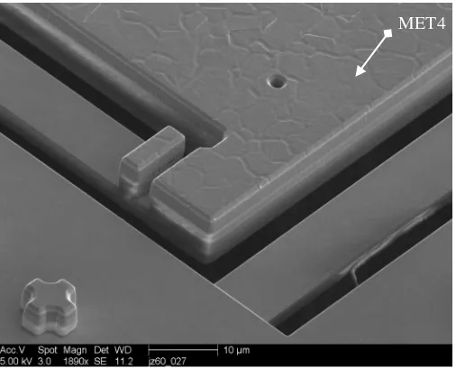
5.6 SEM of the surface roughness in the MET4 layer . . . 70
5.7 Structural figure of merit . . . 71
5.8 Normalized performance variables of the structural figure of merit . . . 72
5.10 Layout detail of the MOEM scanner and electrothermal actuator. . . . 77
5.11 Layout detail of the post-CMOS photomask for the MOEM scanner . . 78
5.12 CMOS-MEMS scanner prototyping . . . 79
5.13 CMOS-MEMS process description in CoventorWare . . . 80
5.14 Virtual layout detail of the MOEM scanner. . . 80
6.1 SEM of the composition of the fabricated CMOS-MEMS scanner . . . . 82
6.2 Curvature of the CMOS-MEMS scanner . . . 83
6.3 State of residual stress in the CMOS-MEMS scanner . . . 85
6.4 Deflection curve of the CMOS-MEMS scanner due to residual stress . . 85
6.5 Geometrical parameters of the CMOS-MEMS actuators . . . 86
6.6 Curvature of the CMOS-MEMS mirror . . . 87
6.7 SEM of a slot in the CMOS-MEMS mirror . . . 90
6.8 Schematic diagram of the electrical measurement setup . . . 91
6.9 Wiring diagram of the electrical measurement setup . . . 92
6.10 Monitored region of interest for functional measurements . . . 94
6.11 Measured quasi-static mechanical response . . . 95
6.12 Computed quasi-static mechanical response. . . 97
6.13 Computed heat transfer by conduction between the comb fingers . . . . 98
6.14 Measured dynamic mechanical response (no offset). . . 100
6.15 Measured dynamic mechanical response (offset) . . . 101
6.16 Extracted cut-off frequencies . . . 102
6.17 Extracted quality factors . . . 104
6.18 Computed mode shapes of the CMOS-MEMS scanner . . . 106
6.19 Computed modal displacements of the CMOS-MEMS scanner . . . 107
6.20 Power sensitivity of the CMOS-MEMS scanner. . . 109
6.21 Measured transient mechanical response . . . 110
6.22 Extracted time constants . . . 111
A.1 Longitudinal heat transfer components in the MOEM scanner . . . 117
B.1 State of residual stress in the CMOS-MEMS test elements 01-02 . . . . 121
B.2 State of residual stress in the CMOS-MEMS test elements 03-08 . . . . 122
B.3 State of residual stress in the CMOS-MEMS test elements 09-14 . . . . 123
B.4 State of residual stress in the CMOS-MEMS test elements 15-20 . . . . 124
B.5 State of residual stress in the CMOS-MEMS test elements 21-26 . . . . 125
B.6 State of residual stress in the CMOS-MEMS test elements 27-30 . . . . 126
B.7 Deflection curves of the CMOS-MEMS test elements 01-06 . . . 127
B.8 Deflection curves of the CMOS-MEMS test elements 07-12 . . . 128
B.9 Deflection curves of the CMOS-MEMS test elements 13-18 . . . 129
B.10 Deflection curves of the CMOS-MEMS test elements 19-24 . . . 130
List of Tables
2.1 Performance comparison of MOEM scanners . . . 13
2.2 Performance comparison of EOCI systems . . . 14
3.1 Thermal boundary conditions . . . 27
3.2 Vibration nodes in a prismatic homogenous cantilever beam . . . 32
4.1 Physical data of CMOS materials . . . 42
4.2 Elements in the CMOS-MEMS test structure TS01 . . . 45
4.3 Elements in the CMOS-MEMS test structure TS11 . . . 45
4.4 Fit parameters for the deflection of the CMOS-MEMS test elements . . 52
4.5 Curvature of the CMOS-MEMS test elements . . . 54
4.6 Theoretical curvature of the CMOS-MEMS test elements . . . 57
4.7 Fit parameters for the rotation of the CMOS-MEMS test elements . . . 58
6.1 Thickness of the CMOS-MEMS scanner. . . 82
6.2 Fit parameters for the deflection of the CMOS-MEMS scanner . . . 83
6.3 Curvature of the CMOS-MEMS scanner . . . 84
6.4 Geometrical parameters of the CMOS-MEMS actuators . . . 86
6.5 Fit parameters for the deflection of the CMOS-MEMS mirror. . . 87
6.6 Curvature parameters of the CMOS-MEMS mirror . . . 88
6.7 Focal parameters of the CMOS-MEMS mirror . . . 89
6.8 Hole width of a slot in the CMOS-MEMS mirror. . . 90
6.9 Electrical resistances of the CMOS-MEMS scanner . . . 93
6.10 Magnitude-frequency relations of the CMOS-MEMS scanner . . . 103
6.11 Cut-off parameters of the CMOS-MEMS scanner . . . 103
6.12 Resonance vibration gains of the CMOS-MEMS scanner . . . 104
6.13 Dynamic parameters of the CMOS-MEMS scanner . . . 105
Chapter 1
Introduction
During the past two decades, the combined application of miniaturization and information technology to biomedical sciences has improved nearly every aspect of health care as well as health research. Specifically, in health care, it has provided better methods for the prevention, diagnostic and treatment of illnesses; in health research, it has led to a more in-depth understanding of pathological processes and physiological functions [1].
This technological integration, together with the advance in underlying disciplines such as electrical, mechanical, optical, physics, materials and computer engineering, has supported a rapid development of novel biomedical instruments with sophisticated functions. As a result, the new instrumentation does not only enable the study of the human body at unprecedented time and space scales but also transforms the manner in which bioinformation is acquired, managed and disseminated.
However, as the required degree of functionality in biomedical instruments in-creases, new challenges arise in the design and fabrication of their components. In the present dissertation, we address the problem of optimizing the thermoelastic actuation system of a microoptoelectromechanical (MOEM) scanner to maximize its operating frequency, while fulfilling the technological constraints of a standard Complementary-Metal-Oxide-Semiconductor (CMOS) microfabrication process. The device is ulti-mately intended to enhance the transverse scanning performance of an endoscopic imaging system.
1.1
Outline
After having introduced the area of study and research topic of the dissertation to the reader, the rest of Chapter 1 provides a background summary of optical co-herence imaging systems, which is the application context of this research work. The full treatment of the research problem is presented in Chapter 2, alongside a concep-tual description of our proposed solution device. The theoretical framework of the physics describing the transduction mechanisms of the proposed device is presented in
device concept as well as a characterization of the residual stress within the involved fabrication materials. Chapter 5discusses the issues involved in the design of the device and its implementation in CMOS technology. Chapter 6 describes, quantitatively, the characteristics of the fabricated CMOS-MEMS scanner; and finally,Chapter 7presents our conclusions.
1.2
Background application
This section summarizes the background of an emerging imaging technique with unique features and promising applications, mainly in clinical medicine and biomedical research.
1.2.1
Optical coherence tomography
Optical coherence tomography (OCT) is a noninvasive imaging technique that generates depth-resolved images of the morphology of a sample by measuring the backscattering or backreflection of light [2]. As its name suggests, OCT exploits the co-herent property of light to determine, in situ and in real time, the optical stratification of highly scattering samples with relatively high depth resolution and high penetration depth.
The maximum achievable values for depth resolution and penetration depth in OCT imaging were, until a couple of years ago, 1 µm and 3 mm, respectively [3]. This sectioning and penetration capability conveniently places OCT as an intermediate alternative between two of the most established imaging techniques, namely, ultrasound (US) and confocal microscopy (CM). In comparison with US, OCT achieves depth resolutions of one to two orders of magnitude higher, but with lower penetration depths; compared with CM, OCT accomplishes penetration depths of one order of magnitude higher, but with lower depth resolutions.
With no other technique imaging within this penetration range and with such reso-lution, OCT rapidly attracted the attention of researchers and clinicians from different specialities, and it therefore became an active development area with many supporting fields and several potential applications.
The following sections briefly explain the principle of operation of OCT and dis-cuss its main imaging modalities. Special attention is devoted to two trends: the combination of OCT with CM, and its application in endoscopy.
1.2.2
Principle of operation
of OCDR, from a one-dimensional (1D) ranging technique to a two- and even three-dimensional (2D, 3D) imaging technique; the last one, also referred to as full-field imaging.
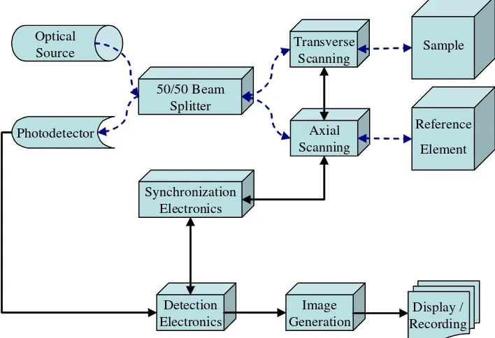
In order to illustrate the principle of operation of OCT, Fig. 1.1 shows the sche-matic diagram of a simplified time-domain OCT system. High-sensitivity detection of OCT signals was demonstrated almost a decade ago using optimal interferometer configurations based on optical circulators [5]. The OCT system of Fig. 1.1 is based on the standard fiber-optic Michelson interferometer (FOMI), which was the original configuration used to demonstrate the OCT technique and is still the most common configuration used in OCT systems by its simplicity [6].
The optical setup of this FOMI-based OCT system consists of an optical source, a 50/50 beam splitter, two scanning stages, and a photodetector. The light is guided through the system via optical fibers and its optical path is as follows: Light emitted by the optical source is coupled into an optical fiber and guided to the 50/50 beam splitter, where it is divided into two identical light beams. One of the beams is guided through one arm of the interferometer to the sample, while the other beam is guided through a second arm to a reference element. Light returning from the sample and reference element is coupled again into the interferometer arms and guided to the 50/50 beam splitter, where these beams are combined to create interference. The combined beam is finally guided out of the system to the photodetector, which measures the time-averaged intensity of this beam.
According to the interferometry theory, the photodetector current provides a
mea-50/50 Beam Splitter
Transverse Scanning Optical
Source
Axial Scanning Photodetector
Synchronization Electronics
Detection Electronics
Sample
Image
[image:19.612.141.495.427.669.2]Generation Recording Display / Reference Element
sure of the correlation between the light returning from the sample and the light re-turning from the reference element. If the interferometer is symmetric, i.e. the sample and reference element have identical optical properties, the photodetector registers the amplitude of the autocorrelation function; otherwise, the cross-correlation amplitude is detected. In either case, the amplitude of the correlation depends on the following parameters: (i) the power of the optical source, (ii) the optical properties of the sample and reference element as well as (iii) the optical path difference between the returned beams. Because the first two parameters are assumed to be time-invariant during an imaging event, the interference phenomenon is essentially associated to the optical path difference between the returned beams. This way, the photodetector registers ampli-tude maxima and minima as the position of the reference element is scanned along the optical axis.
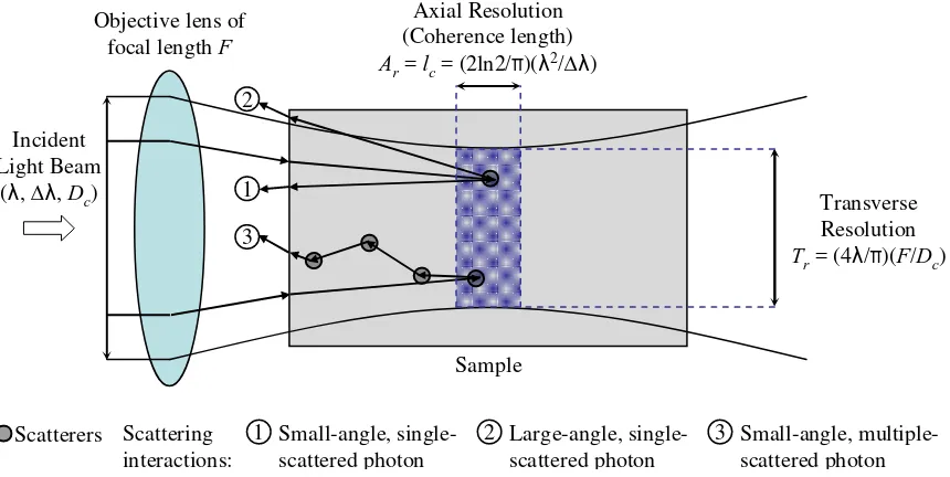
For the ideal case of a symmetric interferometer with perfectly reflecting elements, the temporal coherence theory states that, if the optical source of the system has a broadband spectrum, i.e. a short coherence time according to the Wiener-Khinchin theorem [7], interference will only occur when the optical path difference between the reflected beams is within the coherence length (lc)1 of the optical source; for this reason, an OCT system can resolve the axial position of a reflection site in its sample arm with a resolution that is equal to the coherence length of the optical source [8].
OCT imaging of real samples has demonstrated that this definition of axial reso-lution is also valid for the most general case of a highly scattering sample [9]. However, the penetration depth of an OCT system is strongly limited when multiple reflecting and scattering interactions are considered. This is because, as shown in Fig. 1.2, only single-scattered photons can preserve the coherent phase information and thus con-tribute to the interference signal [10].
The axial imaging capability of an OCT system is therefore determined by the bandwidth of the optical source as well as the optical density of the sample as follows: the more spread the energy is over the frequency domain, the higher the resolution; the less scatterers there are in the sample, the deeper the penetration.
Two noteworthy consequences of the physics describing an OCT system are that the axial and transverse resolution of the system are decoupled and that the system produces heterodyne gain for weak optical signals [11]. These consequences are par-ticularly useful for enabling in vivo imaging of highly scattering tissues at the cellular level [12].
Concerning the electronics components of Fig. 1.1, the detection stage includes an amplifier, a rectifier, and a low-pass filter to demodulate the photodetector signal with the intention of eliminating the noise outside the interferometric bandwidth. Un-desirable noise sources include the detector thermal noise, the 1/f noise, and the noise arising from fluctuations in the power of the optical source [13]. In addition, a syn-chronization stage between the scanning and detection stages is required to guarantee that all imaging events take place, and are recorded and displayed, at the appropriate time and at the correct location.
1
Incident Light Beam
(λ, ∆λ, Dc) Transverse
Resolution Tr= (4λ/π)(F/Dc)
Sample Axial Resolution (Coherence length) Ar= lc= (2ln2/π)(λ2/∆λ) 2
3 1
Scattering interactions:
Scatterers Small-angle, single-scattered photon
1 Large-angle,
single-scattered photon
2 Small-angle,
multiple-scattered photon 3
[image:21.612.107.537.88.304.2]Objective lens of focal length F
Figure 1.2: Coherence length and scattering interactions within a sample analyzed with a FOMI-based, time-domain OCT system in a pre-objective scanning configu-ration. In this configuration, λ and ∆λ are the center wavelength and full-width-at-half-maximum of the power spectrum of the optical source (which is assumed to be Gaussian); Dc is the diameter of the collimated Gaussian beam being scanned.
1.2.3
Imaging modalities and scanning protocols
The first demonstrated imaging modality in OCT systems was conceptually similar to the ultrasound (US) B-mode imaging except that OCT used light instead of sound [2]. This initial mode of imaging allowed to generate 2D, cross-sectional images by performing successive rapid axial measurements of backscattered or backreflected light at different transverse positions, as illustrated in Fig. 1.3, and then displaying the measurements as intensity maps over the axial and transverse positions.
Subsequent developments in OCT imaging modalities included the addition of parallel and orthogonal image planes as well as the prioritization of scanning measure-ments [13–17]. Considering an OCT system equipped with three 1D, linear scanners and orthogonal scanning axes, Fig. 1.4shows the different scanning protocols that can be used to obtain volumetric information about a sample. The size of the measurement spots, and consequently the separation between image planes, is determined by the product of the axial and transverse resolution defined in Fig. 1.2.
Incident Light Beam
T
ra
ns
ve
rs
e
P
os
it
io
n
Axial Position (Depth) Scanning lines
(a)
B
ac
kr
ef
le
ct
ed
o
r
B
ac
ks
ca
tt
er
ed
I
nt
en
si
ty
Axial Position (Depth)
(b)
Figure 1.3: OCT B-mode imaging based on axial scans (A-scans): (a) axial scanning lines and (b) measurement traces. Measurement traces represent the optical backscattering or backreflection profile along axial scanning lines in the sample being imaged.
Fig. 1.4(c)and Fig. 1.4(d)show that the same image planes of the A-scans based B-mode imaging can be acquired with a mid-transverse scanning priority, i.e. the scan frequency in the axial direction fz is higher than the scan frequency in one transverse direction fx or fy but lower than the scan frequency in the other transverse direction. This modality is referred to as T-scans based B-mode OCT imaging.
DEPTH PRIORITY fz> fx> fy
y x
z
Incident Light Beam
(a)
DEPTH PRIORITY fz> fy> fx
y x
z
Incident Light Beam
(b)
MID TRANSVERSE PRIORITY fx> fz> fy
y x
z
Incident Light Beam
(c)
MID TRANSVERSE PRIORITY fy> fz> fx
y x
z
Incident Light Beam
(d)
FULL TRANSVERSE PRIORITY fx> fy> fz
y x
z
Incident Light Beam
(e)
FULL TRANSVERSE PRIORITY fy> fx> fz
y x
z
Incident Light Beam
(f)
Chapter 2
Research Problem
This chapter discusses and proposes a solution to the problem of implementing a high-speed, high-fidelity, full-field endoscopic optical coherence imaging (EOCI) system. The discussion is based on a literature review of the state-of-the-art research done to address this particular problem. The aim of this section is to expose the areas in which miniaturization technology could be used to enhance the performance of the EOCI system.
2.1
Problematic situation
The quest for higher frame rate and better image fidelity, i.e. higher resolution and wider spatial range, remains the cornerstone of OCI systems; and, in general, of any medical imaging system. Moreover, when endoscopic applications of OCI systems are desired, the size of the optical components in the sample arm becomes an additional concern because of the limited space in the probe. What is more important to this quest, however, is that any applied technology to this area must evidence its diagnostic utility and be cost-effective for users.
Discussing image fidelity first, it was explained inSection 2.1.1that optical sources with broadband spectrums could be used to improve the axial resolution of an OCI system. Likewise, the use a high numerical aperture (NA) lens in the scanning probe improves transverse resolution, but also decreases the depth of focus [13, 18]. Hence, a tradeoff exists between transverse resolution and imaging depth. This tradeoff is illustrated in Fig. 2.1 for the case of a weak- and strong-focusing system. Fig. 2.1(a)
Low NA Lens
Transverse Resolution Incident
Light Beam
Axial Resolution
Depth of Focus
(a)
High NA Lens
Transverse Resolution Incident
Light Beam
Axial Resolution
Depth of Focus
(b)
Figure 2.1: Schematic illustration of focusing optics in the scanning probe of an OCI system: (a) weak and (b) strong focusing. The size of the imaging zone is determined by the product of axial and transverse resolution.
2.1.1
Approaches to high-fidelity OCI systems
Several approaches have been suggested to overcome the tradeoff between reso-lution and spatial range; and consequently, to enable OCI with depth-independent transverse resolution. Typical approaches employ focusing compensation techniques [19–26] or deconvolution methods [27–29], whereas research-grade approaches employ axicon lenses [30, 31].
Focusing compensation techniques are in turn based on dynamic focus tracking methods [19–24] or on zone-focusing and image-fusion methods [25,26]. Dynamic focus tracking methods seek to synchronously scan the position of the coherence gate with the position of the focal plane in order to maintain optimal focusing conditions over the entire imaging range. In these methods, synchronization is achieved either by mounting conventional optical elements, such as spherical lenses, mirrors or prisms, on a single scanning stage [19–22] or by sequentially activating adaptive optical elements, such as deformable lenses [23] or mirrors [24]. Zone-focusing and image-fusion methods, on the other hand, concentrate on postprocessing of OCI data. In these methods, multiple images are acquired with different positions of the focal plane, while the coherence gate is maintained at a fixed position; in-focus image zones are then numerically fused to create high-fidelity images. These methods require several scannings of the sample with full transverse priority [25,26].
Deconvolution methods also involve numerical postprocessing of OCI data. In these methods, deconvolution algorithms are used to correct defocusing distortions outside the confocal region; e.g. axial defocusing correction is implemented with the constrained iterative restoration algorithm [27] and transverse defocusing correction is implemented with focal- or depth-dependent algorithms [28, 29].
the far field of these lenses [31].
Although single-focused Bessel beams allow OCI with uniform and optimal trans-verse resolution over the entire depth of focus, which can be as long as 6 mm for a transverse resolution of 10µm [30], their focal intensity is about 17 times less than the intensity of Gaussian beams. Moreover, when detection is performed along the reverse path through the same axicon lens, their focal intensity drops to even lower values. As a result, this approach overcomes the image fidelity problem, but at the price of lower detection sensitivities. Concerning double-focused Bessel beams, they have been used to decouple the illumination and detection paths in an axicon lens as a strategy to maintain the intrinsic high detection sensitivity of OCI systems [31]. However, even though this approach also allows OCI with uniform and optimal transverse resolution, it does not achieve the same extended depth of focus obtained with the single-focused Bessel beams.
In general, there are several drawbacks to these approaches; e.g. focusing compen-sation techniques are typically based on bulky optical elements, which limit the tracking speed and preclude their application in high-speed, EOCI systems. Zone-focusing and image-fusion methods also suffer from slow frame rates and space limitations in the probe due to bulk optics designs, plus both previous approaches require complex elec-tronic control systems to synchronize the axial and transverse scanning stages. Approa-ches that are based on numerical postprocessing of OCI data, such as zone-focusing and image-fusion methods and deconvolution methods, demand high signal-to-noise ratios and hence, expensive detection electronics or high-power sources; the last one, compro-mising patient safety. Lastly, as explained earlier, approaches based on axicon lenses also have disadvantages of low detection sensitivities and bulky optical elements.
2.1.2
Approaches to high-speed EOCI systems
Recently, the microelectromechanical systems (MEMS) technology has been in-corporated into the EOCI systems to facilitate endoscopic beam steering and to com-pensate for defocusing distortions. MEMS-based components for EOCI systems have received considerable attention because of their capability to miniaturize large-scale systems without loss of functionality, integrate heterogenous systems into single mono-lithic devices, exploit new physical domains, increase operation speed as well as decrease power consumption and manufacturing cost; especially, when compared with large-scale components.
Table 2.1 and Table 2.2 summarize the state of the art in the use of MEMS-based components for EOCI systems. Table 2.1 shows a performance comparison of the microoptoelectromechancial (MOEM) scanners reported in the literature during the past decade. The reported devices are compared in terms of three performance variables: mechanical output, electrical input and operation speed. The actuation parameters, such as principle of operation, active materials and topology, as well as the reflective material and reflective area of each device are also provided for reference.
resolution and imaging speed are reported for comparison. In addition, the scanning dimension and scanning modality are provided for reference.
Upon qualitative analysis ofTable 2.1, it is easy to note that the prevalent actua-tion principles in the reported MOEM scanners are electrostatic and electrothermal. This prevalence can be attributed to the ease of implementing these actuation princi-ples using the standard materials in MEMS technology, i.e. silicon (Si), either amor-phous silicon (aSi), single crystalline silicon (scSi) or polycrystalline silicon (polySi), and silicon-based materials such as silicon oxides (SiOx), silicon nitrides (SiNx), silicon oxynitrides (SiNxOy), silicon carbides (SiCx), germanium (SiGe) and silicon-germanium-carbon (SiGeC); which are also the predominant materials in the micro-fabrication processes of the integrated circuits (IC’s), from which MEMS technology evolved.
Moreover, as Table 2.1 again shows, the MOEM scanners based on these actua-tion principles exhibit the highest mechanical outputs as well as the highest operaactua-tion speeds, as it can be seen from [32–34] and [35–37], respectively. A closer comparison of the performance variables reveals that electrothermal actuation is the most suitable principle for large displacement applications, while electrostatic actuation is the most suitable principle for high speed applications.
Table 2.1: Performance comparison of MOEM scanners for EOCI.
Publication Actuation Mirror Scanning performance
Reference Year Principlea Materials Topologyb Material Area (mm×mm) θ/ ∆z I/ V f, Hz
[38, 39] 2001,2003 ET SiO2-polySi-Al BTA Al 1×1 17o 15 mA 165
[40, 41] 2002,2003 ES polyimide IFA Au 1.5×1.5 3.1o 50 V 4
[42] 2003 ES SiO2-polySi-Al CHCD Al 1×1 9.4o 18 V 233
[43, 44] 2003 ET SiO2-polySi-Al BTA Al 1×1 37o 7.5 mA 165
[36] 2004 ES Si3N4 PPD Au 1×1.4 1 µm 400 V 4,000
2004 ET SiO2-polySi-Al 2OA-BTA Al 1×1 40
o 6.3 mA / 15 V 445
[33]
25o 8 mA / 17 V 259
2005 ES Si3N4 2OA-PPD Al 1×1 40.11
o
100 V 45
[32]
27.22o 181
2005 ET SiO2-polySi-Al 2PA-BTA Al 0.7×0.32 200µm 6 V 2,620
[37]
1,180
2005 ES scSi 2OA-BCD Au 0.6×0.6 30o 100 V 8,000
[35]
3,500
2005 ET SiO2-polySi-Al 2PA-BTA Al 0.2×0.2 280µm 12 mA / 10 V 2,150
[34]
1,100
2006 EM Au-polyimide-Cr 2OA-TA Au 2.2×6.4 4.4
o 20 mA 322
[45]
2.7o 27 mA 236
2007 ES polySi 2OA-AVCD Au diameter: 1 6o 100 V 463
[46]
140
2007 ES scSi 2OA-GLVCD scSi NRc 20o NRc 1,800
[47]
2,400
2007 EM NdFeB 2OA-FFH Au 0.6×0.8 20o 3 V 450
[48]
350
[49] 2008 ET scSi-AL 2OA-GLBTAFS Au-Cr diameter: 0.5 17o 1.3 V 46
aET:electrothermal, ES:electrostatic, EM:electromagnetic.
bBTA:bimorph thermal actuator,IFA:integrated force array, CHCD:curled-hinge comb drive, PPD:parallel plate drive,
2OA-BTA:two-orthogonal-axis bimorph thermal actuator, 2OA-PPD:two-orthogonal-axis parallel plate drive, 2PA-BTA:two-parallel-axis bimorph thermal actuator,2OA-BCD:two-orthogonal-axis bending comb drive,
2OA-TA:two-orthogonal-axis torsional actuator,2OA-AVCD:two-orthogonal-axis angular vertical comb drive,2OA-GLVCD:
two-orthogonal-axis gimbal-less vertical comb drive,2OA-GLBTAFS: two-orthogonal-axis gimbal-less bimorph thermal actuator
with flexural spring2OA-FFH:two-orthogonal-axis folded flexure hinge.
cNR:not reported in original publication.
Table 2.2: Performance comparison of EOCI systems based on MOEM scanners.
Publication Scanning Imaging performance
Reference Year Dimensions Modality Range T×A (mm×mm) ResolutionTr /Ar (µm/µm) Speed (frames/s)
[38, 39] 2001,2003 2D B-mode based on A-scans 2.9×2.8 20 / 10.2 5
[40, 41] 2002,2003 2D B-mode based on A-scans 2.75×3 x / 20 4-8
[42] 2003 2D NRb
[43, 44] 2003 2D B-mode based on A-scans 4.2×2.8 20 / 10.2 5
[36] 2004 2D FCa based on C-mode 0.5×1.25 50 / 13 0.05
[33] 2004 3D NRb
[32] 2005 3D B-mode based on A-scans 0.7×0.2×1 35 / 13 0.5
[37] 2005 1D A-scan A: 0.2 A: NRb 5,200 lines/s
[35] 2005 3D B-mode based on A-scans 2×2×1.4 20 / 10 3-5
[34] 2005 1D FCa based on A-scans A: 0.28 A: 2 2,000 lines/s
[45] 2006 3D B-mode based on A-scans 8×8×1.4 10 / 17 0.0175
[46] 2007 3D C-mode 1.8×1×1.3 12 / 4 0.0123
[47] 2007 3D B-mode based on A-scans 1×1×1.4 20 / 10 0.067
[48] 2007 3D B-mode based on A-scans 1×2.3×1.5 23 / 11.27 0.1852
2008 3D B-mode based on A-scans 0.55×0.55×1 20 / 12 21.5c
[49]
C-mode
aFC:focus compensation.
bNR:not reported in original publication.
cThis rate meets the requirements of the video rate imaging.
2.2
Proposed solution model
This section describes the MOEM scanner proposed in this dissertation. The section first explicates the intention in developing the device and then illustrates its topology.
2.2.1
Purpose of the MOEM scanner
The dissertation proposes to develop a MOEM scanner with the intention of in-creasing the transverse scan frequency of a time-domain, full-field optical coherence imaging (OCI) system.
The scanner will rely on the reflection operation principle to modify the propaga-tion direcpropaga-tion of a Gaussian incident laser beam over a 3D sampling space by using serial processing of light. Reflection-type scanners are selected over refraction- or diffraction-type ones because of their performance characteristics such as high deflection angles (≈ 100 o), high scan rates (≈100 kHz), very high optical efficiencies (≈95 %), good long-term stabilities, multi-dimensional scanning capabilities and wavelength independence [50].
The proposed MOEM scanner (Fig. 2.2) is a conceptual evolution of the CMOS-compatible micromirror developed by Pan et al. in 2001 [38]. In this case, the research activity is focused on the study of temperature-gradient actuation schemes and higher-order vibrational modes in the device with the intention of performing high-speed, dual scanning operation.
2.2.2
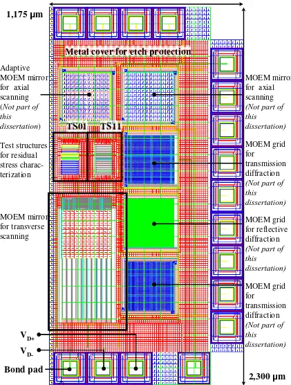
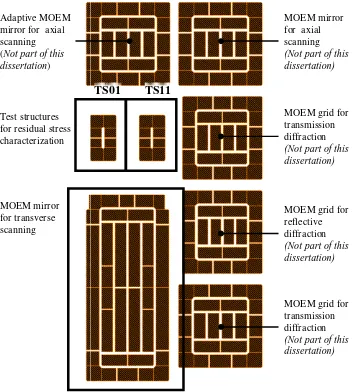
Topology of the MOEM scanner
The topology of the MOEM scanner for transverse scanning applications includes aLm×Lmsquare mirror plate supported at one side by an array ofnbparallel cantilever (fixed1-free) beams with rectangular geometry2 (L
b×Wb) as shown inFig. 2.2(a). Note that, for this topology and scanning application, the optical plane of incidence must be found in the x-z plane.
A second array of nf parallel beams with rectangular geometry (Lf × Wf) is attached at the free end of the mirror plate; which in conjunction with a third array of nf + 1 parallel cantilever (free-fixed3) beams of identical dimensions, form a comb-type capacitive sensing structure as shown in Fig. 2.2(a)and Fig. 2.2(d). The purpose of this sensing structure is to provide feedback to an electronic controller about the actual scan frequency, and hence operating the device at optimal resonance conditions, i.e. within the resonance frequency band.
1
The supporting beams are fixed to the substrate through the frame member.
2
Previous experimental work reported in [43,44] has demonstrated that this beams arrangement eliminates the adverse hysteresis effect caused by thermal relaxation and wobbling occurred in earlier designs [38,39].
3
Lr
Lb Lm
Wr
Lo Lf
A A’
Frame
Wb gb
Wf gf
x y
z B
B’
x’ y’
z’ C
C’
Substrate Layers: Oxide Heating Metal
(a)
Lb Lm Lf
x z
y Cx
t2 t3
t1 Lm/2
x’ z’ y’
Substrate Layers: Oxide Heating Metal
(b)
Wb t2
y z
x
Wr gr Wr DR1 DR1
Oxide Heating Metal Layers:
t3
t1
(c)
gf
Wf Wf Wf Wf Wf
gf gf gf
y’ z’
x’
t3
t1
Oxide Metal Layers:
(d)
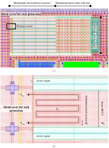
Fig. 2.2(b), Fig. 2.2(c) and Fig. 2.2(d) expose the composite structure of the de-vice, which contains a high-reflective metal layer stacked over a bottom oxide layer. In addition, a set of meander heating resistor are embedded within the bottom layer of each supporting beam to form the electrothermal actuation system as shown in
Fig. 2.2(a), Fig. 2.2(b) and Fig. 2.2(c). This way, when an electrical signal is applied to the resistors, the supporting beams bend around theyaxis as a result of the dissimi-lar thermoelastic response of composing layers to Joule heating phenomenon and both, out-of-plane and tilting movement are transferred to the mirror plate.
Fig. 2.2(a) depicts a single-meander resistor for illustrative purposes only; but in general, a meander resistor, such as the one shown in Fig. 2.3(a), can be in turn composed of annm number of single-meander resistors. Fig. 2.3 shows that this exem-plary three-meander resistor can be separated for analysis into two elemental resistors, namely, a rectangular and a single-meander resistor. The respective effective lengths of these elemental resistors can be obtained from Fig. 2.3(b) and Fig. 2.3(c) as Lr/2 and Lr −2Wr+gr+ 2(0.559)Wr, where Lr and Wr are the span length and width of the more general resistor; 0.559 is the correction factor for a bend due to the change in current density at its right-angle path.
Therefore, the effective length of an nm-meander resistor is given by
Le = 2 [Lr/2] +nm[Lr−2Wr+gr+ 2(0.559)Wr], (2.1)
or, equivalently, by
Le = Lr(1 +nm) +nm(gr−0.882Wr). (2.2)
Lr
Wr
Bend
Bend Bend
Bend Bend Bend
Wr
Wr
Wr gr gr
Lr- 2Wr Wr Wr
Terminal
gr
Terminal
(a)
Wr
Lr/2
Terminal
(b)
Wr
Lr/2 - Wr
Bend
Bend
Wr gr
Wr
Lr/2
(c)
Chapter 3
Theoretical Framework
This chapter presents a theoretical framework of the physics describing the trans-duction mechanisms of the proposed MOEM scanner. The chapter first introduces a multimorph formulation to assess the effective value of the materials properties of a composite structure and then analyzes both the static and dynamic electrothermal behavior of composite actuators.
3.1
Material properties of composite structures
Structures that are fabricated of more than one material are called composite structures. A composite structure can be treated as an anisotropic material because some of its effective material properties, such as electrical, mechanical and thermal properties, depend on the direction considered [51]. The analysis of composite struc-tures is important because, as it will be explained in Chapter 4, most MEMS are formed from stacked material layers, and thus both their material properties and mo-deling equations must be expressed in terms of their respective effective or multimorph counterparts in order to improve the accuracy of the predicted results.
The following analysis considers the prismatic, layered composite structure shown in Fig. 3.1. The structure consists of N different elastic material layers, each one denoted by the index i and with unique thickness and material properties. The total thickness of the structure is t and its length and width are L and W, respectively. Consequently, all material layers have the same surface area AS = LW but different transverse (AT i=Lti) and cross-sectional (Ai =W ti) area.
The effective value of the material properties that are directly involved in the electrothermal behavior of the analyzed composite actuators are defined as follows:
Mass density
Mathe-L
t
t
Nt
N-it
2t
1W
Figure 3.1: Generic geometry of an elastic, prismatic, layered composite beam.
matically, this is expressed as
ρ = 1
t i=N
X i=1
ρiti. (3.1)
Heat capacity
The effective specific heat capacity of the composite beam (c) can be obtained by weighting the specific heat capacity of each layer (ci) by the respective surface mass density (ρiti); i.e.
c = 1
ρ t i=N
X i=1
ciρiti. (3.2)
Thermal conductivity and resistivity
The effective thermal conductivity of the composite beam along its longitudinal direction (kL,T h) can be obtained as the thickness-weighted average of the thermal conductivity of each layer (kT hi); i.e.
kL,T h = 1
t i=N
X i=1
kT hiti. (3.3)
The effective longitudinal thermal resistivity of the composite beam is given by
̺L,T h = 1
kL,T h
. (3.4)
Similarly, the effective thermal resistivity across the thickness of the composite beam (̺t,T h) can be obtained as the thickness-weighted average of the thermal resistivity of each layer (̺T hi); i.e.
̺t,T h = 1
t i=N
X i=1
The effective transverse thermal conductivity of the composite beam is given by
kt,T h = 1
̺t,T h
. (3.6)
3.2
Static behavior of electrothermal composite
ac-tuators
3.2.1
Mechanical stress deformation
Deflection curve
The deflection curve of an elastic structure, such as the beam depicted in Fig. 3.1, describes the deformation profile along its longitudinal axis as a result of applied loads. These loadings also determine the curvature κ of the structure, which represents the rate of change of the angle of rotationθwith respect to the distance along the deflection curve and, in cartesian coordinates, is expressed as
κ =
d2 w(x) dx2
1 + dwdx(x)2
3/2, (3.7)
where w is the deflection curve, i.e. the out-of-plane displacement of any point on the longitudinal axis of the structure, and dw / dx = θ.
The exact solution to (3.7) has been obtained for many different types of beams and loading conditions since Euler solved the problem of the elastica for both large and small deflections [52]. For discussion purposes, the next analysis expresses the mathematical solution to(3.7) for large deflections of a cantilever beam with a vertical load at its free end in terms of the following elliptic integral of the first kind [53]
Z θ 0
dt
q
sin (θ) − sin (t) = √
2L κ, (3.8)
where t is a dummy variable of integration and L is the length of the beam. In the case of small deflections, the square of the slope in (3.7) is assumed to be very small compared to unity. Hence, the differential equation for curvature can be reduced to the linear caseκ = d2w / dx2, yielding a closed-form solution for the angle of rotation given by [54]
θ = L κ /2, (3.9)
where θ is evaluated at x=L.
0 5 10 15 0
0.5 1 1.5
Dimensionless factor, L κ
Angle of rotation,
θ
(rad)
Large deflection Small deflection
(a)
0 5 10 15
100 102 104
Dimensionless factor, L κ
Relative percentage error, RPE
θ
(%)
(b)
Figure 3.2: Angle of rotation of a cantilever beam: (a) solution for large and small deflections and (b) relative percentage error of the solution.
using the recursive adaptive Lobatto’s quadrature rule [55] with a tolerance of 1×10⁻⁶
.
Fig. 3.2(b) shows that the exact solution of the rotation angle can be approximated by the linear solution with an error less than 10 % for angles inferior to 0.5021 rad (28.77o).
Elastic bending
According to the Euler-Bernoulli beam theory, when a linear, isotropic elastic beam is subjected to a pure bending moment M. i.e when the shear force acting on the beam is equal to zero, it is known that axial lines bend to form circumferential lines and transverse lines remain straight and become radial lines as shown in Fig. 3.3(b). Therefore, a neutral surface must exist that is parallel to the top and bottom surfaces of the beam and for which the length does not change.
The deformation of the beam due to the bending moment is then related to the curvature of the neutral surface as follows:
κ ≡ 1 rc
= M
E I, (3.10)
where rc is the radius of curvature of the neutral surface and the E I product is the flexural rigidity of the beam [56]. Eqn. (3.10) can be applied to composite beams too since, as in one-material beams, the assumption that their cross sections remain plane during pure bending is also valid.
L
t
(a)
Neutral surface
rc= 1 / κ
θ
t0 M M’
(b)
Figure 3.3: Schematic view of the plane of symmetry of a linear, isotropic elastic beam: (a) initial and (b) bent configuration.
direction.
Position of the neutral surface
The position of the neutral surface (t0) in a layered composite beam subjected to in-plane loadings can be obtained as the modulus-weighted centroid of the beam [57]; i.e.
t0 = PN
i=1 R
AiEiz dAi
PN i=1
R
AiEidAi
, (3.11)
where Ei and Ai are the elastic modulus and cross section of the ith material layer, respectively; N is the number of composing material layers and z is the out-of-plane coordinate with respect to the neutral surface.
Elastic moduli
The exact value of Ei in (3.11) depends on the nature of the plane stress being applied. For uniaxial stress,Ei is the uniaxial elastic modulus, or Young’s modulus; for biaxial stress, ˆEi =Ei/(1−νi) is the biaxial elastic modulus, where νi is the Poisson’s ratio of the ith material layer.
These elastic moduli can be expressed in terms of the normal strains (ǫxi, ǫyi and ǫyi) and normal stresses (σxi, σyi and σzi) in each material layer using the Hooke’s law for plane stress. In the case of biaxial stress with σz = 0,
ˆ
Ei =
σxi − νiσyi ǫxi
= σyi − νiσxi
ǫyi
= − σxi + σyi
ǫzi
in the case of uniaxial stress with σy = 0 and σz = 0,
Ei = σxi ǫxi
= − σxi
ǫyi
νi = − σxi
ǫzi
νi. (3.13)
Flexural rigidity
The effective flexural rigidity of a layered composite beam subjected to in-plane loadings can be obtained as the summation of the flexural rigidity of each material layer and is given by
E I = N X i=1
EiIi = N X i=1
Z Ai
Eiz2dAi, (3.14)
where Ii is the moment of inertia of the ith cross-sectional area with respect to the y axis.
Bending moment
The stress-induced bending moment about the neutral surface of a layered com-posite beam is given by
My = N X i=1
Z Ai
σiz dAi, (3.15)
whereσi is the normal stress acting over the cross section of theith material layer and z is the out-of-plane coordinate across the thickness of the beam, with an origin chosen at its neutral surface, i.e. z = 0.
Stresses
Residual stresses: Nearly all thin film materials are found to be in a state of residual stress, regardless of the means by which they were produced [58]. Therefore, it is expected that the proposed device has an initial bending moment as a result of the residual stresses developed during its microfabrication process. This initial bending moment will place the device in a rest position, out of the originally horizontal-considered plane (shown inFig. 2.2(b)). The rest position depends on the geometry, materials and process conditions of the device; but once the device is fabricated, the bending moment that cause it, will remain constant through actuation. A mathematical description of the residual stress state within a thin film is given by (4.3) and it will be discussed later in more detail inSection 4.3.
Thermal stresses: These stresses are a consequence of the thermal expansion of mate-rials. In an uniaxial elastic consideration, the thermal stress within an unreleased monolayer material is given by
σT h = E α∆T, (3.16)
where E and α are the Young’s modulus and coefficient of thermal expansion of the material, respectively; ∆T = T −T0 is the uniform temperature variation from the reference temperature T0 [58]. As (3.16) shows, thermal stresses are independent of the geometry of the device, but depend on materials properties. Moreover, when a composite structure is subjected to a temperature variation, the thermal stress difference between composing layers is amplified, leading to relatively large mechanical deformations of the device [58].
3.2.2
Steady-state temperature distribution
The temperature variation distribution (∆T) in steady-state conditions within the layered composite structure shown in Fig. 3.4 can be determined by solving the following heat transfer equations derived inAppendix A.1
d2∆T dx2 − Υ
2
1∆T = Υ, for 0 ≤ x ≤ Lr, (3.17)
d2∆T dx2 − Υ
2
2∆T = 0, for Lr ≤ x ≤ Lb, (3.18)
d2∆T dx2 − Υ
2
3∆T = 0, for Lb ≤ x ≤ Lb +Lm, (3.19)
where Lr, Lb and Lm are the span lengths of the embedded resistor, supporting beam and mirror plate section, respectively; Υ, Υ1, Υ2and Υ3are constant coefficients defined as
Υ ≡ −̺El,0J 2W
rtr kT h,rWbt
Lb Lm Lf
x z
y
tr
t
Substrate Layers: Oxide Heating Metal Thermal contacts
T0 Fixed temperature
Thermal insulation
T =T0
RTh,ks RTh,kf
T
T0
w0
w
δδδδw
Rotor at T(Lb+Lm)
Stator at T0 RTh,c
Lr
Figure 3.4: Schematic description of the electrothermal model for the MOEM scanner. The solid lines represent heat-loss paths by conduction and the dashed lines represent heat-loss paths by convection (Heat loss by radiation is neglected).
Υ21 ≡ βElΥ +
2hc(Wb+t) kT h,rWbt
, (3.21)
Υ2
2 ≡
2hc(Wb +t) kT h,bWbt
, (3.22)
Υ23 ≡ 2hc
kT h,mt
, (3.23)
where ̺El,0 is the electrical resistivity of the ohmic heating layer at a reference tempe-ratureT0,βEl is the linear temperature coefficient of electrical resistivity of the heating layer, J is the current density flowing through the cross-sectional area (Ar =Wrtr) of the heating resistor, hc is an effective heat transfer coefficient1; kT h,r, kT h,b and kT h,m are the effective thermal conductivities of the composite sections along the longitudinal direction of the structure2; W
r and Wb are the widths of the heating resistor and beam section of the structure, respectively; tr andt are the thickness of the heating layer and composite structure, respectively.
The respective solutions to(3.17), (3.18)and (3.19)are the following
∆T(x) = Γ1 sinh(Υ1x) + Γ2 cosh(Υ1x) + Γ3, for 0 ≤ x ≤ Lr, (3.24)
∆T(x) = Γ4 sinh(Υ2x) + Γ5 cosh(Υ2x), for Lr ≤ x ≤ Lb, (3.25)
1
An effective heat transfer coefficient is used in this model to account for combined heat loss from the structure surface, including convective heat transfer to the surrounding ambient air atT∞ =T0
(RT h,c) and conductive heat transfer through the air to the substrate at T0 (RT h,ks).
2Note that it follows from (3.3) that when the structure has uniform materials throughout, as
Table 3.1: Thermal boundary conditions of the MOEM scanner.
Label Interface Description Mathematical terminology Type Equation
TBC1 x= 0 Fixed temperature Dirichlet ∆T(0) = 0
TBC2
x=Lr Thermal contact Mixed
∆T(Lr) = ∆T(Lr)
TBC3 kT h,rd∆dxT(Lr) = kT h,bd∆dxT(Lr)
TBC4
x=Lb Thermal contacta Mixed
∆T(Lb) = ∆T(Lb)
TBC5 Wbd∆dxT(Lb) =Wm∗d∆dxT(Lb)
TBC6 x=Lb+Lm Thermal insulationb Neumann d∆dxT(Lb+Lm) = 0
aThe symmetry of the temperature field in the device allows to considerW∗
m=Wm/nb, whereWm =Lm is the width of the mirror plate andnb is the number of supporting beams, as shown in Fig. 2.2(a).
bThe temperature distribution is assumed to be uniform along the rotor comb fingers and the conductive heat transfer through the air from the rotor to the stator comb fingers is neglected.
∆T(x) = Γ6 sinh(Υ3x) + Γ7 cosh(Υ3x), for Lb ≤ x ≤ Lb+Lm,(3.26)
where Γ1, Γ2, Γ3, Γ4, Γ5, Γ6 and Γ7 are constants of integration.
The third constant can be obtained by substituting(3.24)into(3.17), which yields to
Γ3 = − Υ Υ2 1
. (3.27)
The six other constants are determined by the thermal boundary conditions of the device, which are summarized inTable 3.1.
In this manner, it follows from the application of TBC1 that
Γ2 = −Γ3 = Υ Υ2 1
; (3.28)
the subsequent application of TBC2 to TBC6 results in a system of linear equations, which can be written in matrix from as
where
MΥ =
sinh1,r −sinh2,r −cosh2,r 0 0
kT h,r kT h,b
Υ1
Υ2 cosh1,r −cosh2,r −sinh2,r 0 0
0 sinh2,b cosh2,b −sinh3,b −cosh3,b
0 Wb
W∗
m Υ2
Υ3 cosh2,b Wb W∗
m Υ2
Υ3 sinh2,b −cosh3,b −sinh3,b
0 0 0 cosh3,b+m sinh3,b+m
, ~
Γ = h Γ1 Γ4 Γ5 Γ6 Γ7 iT
,
~vΥ = h Υ
Υ2
1 (1 − cosh1,r) − kT h,r kT h,b
Υ
Υ1Υ2 sinh1,r 0 0 0
iT
.
Note that a shorthand notation has been introduced in the previous relations to designate the argument of the hyperbolic functions, i.e. fι,±ℓ ≡f(ΥιL±ΥιLℓ).
The column vector of yet unknown constants of integration (~Γ) is then given by
~
Γ = M−1
Υ × ~vΥ, (3.30)
where M−Υ1 is the inverse matrix of MΥ.
The exact expressions of the elements in~Γ are lengthy and instead their ratios are reported:
Γ1 Γ2
= −Γ1 Γ3
= −sinh1,r ΓA + (cosh1,r −1) ΓB cosh1,r ΓA + sinh1,r ΓB
, (3.31)
Γ4 Γ5
= −WbΥ2 sinh2,b cosh3,m +W
∗
mΥ3 cosh2,b sinh3,m WbΥ2 cosh2,b cosh3,m +Wm∗ Υ3 sinh2,b sinh3,m
, (3.32)
Γ6 Γ7
= −tanh3,b+m, (3.33)
where,
ΓA = kT h,rΥ1(WbΥ2 cosh2,b−r cosh3,m +W ∗
mΥ3 sinh2,b−r sinh3,m), (3.34)
ΓB = kT h,bΥ2(WbΥ2 sinh2,b−r cosh3,m +W ∗
mΥ3 cosh2,b−r sinh3,m). (3.35)
boundary condition
kT h,mW
∗
mt d∆T
dx (Lb+Lm) =kT h,air
nfWfLf
δw ∆Tf, (3.36)
where ∆Tf = ∆T(Lb+Lm) is the uniform temperature variation distribution along the rotor comb fingers, δw = w0 −w(∆Tf) is the varying air gap between the rotor and stator comb fingers during actuation, where w0 is the initial out-of-plane displacement at the centroid of the rotor comb fingers due to residual stresses developed during its microfabrication process and w(∆Tf) is the temperature-dependent, out-of-plane displacement at the centroid of the rotor comb fingers due to thermal stresses developed during its actuation; kT h,m = kT h,b is the effective, longitudinal thermal conductivity of the composite section of the device without embedded resistor and kT h,air = 0.0024 W/K/m is the thermal conductivity of the air [57]; W∗
m and t are the respective width per supporting beam and thickness of the mirror plate;nf,Wf andLf are the respective number per supporting beam, width and length of the rotor comb fingers.
The application of the thermal boundary condition described by (3.36)leads to a reformulation ofMΥ and~vΥ in(3.30), which finally yields to
Γ6 Γ7
= kT h,bW
∗
mtΥ3 cosh3,b+m −kT h,airnfWf Lf sinh3,b+m / δw kT h,airnfWfLf cosh3,b+m / δw − kT h,bWm∗ tΥ3 sinh3,b+m
. (3.37)
It is noteworthy that the, in order to use (3.37), an iterative electrothermomecha-nical model for the device is required, as it is necessary to solve both the heat transfer equations and the thermally-induced mechanical deformation.
3.2.3
Electrothermal coupling
As it was detailed in Appendix A.1, the electrical and thermal domains of the device are coupled by Joule’s first law, i.e. the embedded ohmic resistors transduce the electrical input power into heat according to the following equation
˙
qg = dQ˙g
dV = ̺ElJ
2, (3.38)
where ˙qg is the heat generated per unit time ( ˙Qg) per unit volume (V) by a single ohmic resistor,̺Elis the electrical resistivity of the ohmic material andJis the current density flowing through the cross-sectional area (Ar) of this resistor.
In steady-state conditions, Maxwell’s equations imply that J is proportional to the negative gradient of the electric potential (ϕ) and is given by
−
→J = −−→∇ϕ ̺El
. (3.39)

![Figure 5.12: Prototypes of the CMOS-MEMS scanner: (a) scanning electron mi-crograph of the fabricated CMOS-MEMS scanner [Equipment: FEI Sirion scanningelectron microscope] and (b) corresponding 3D virtual model [Software: Coventor-Ware].](https://thumb-us.123doks.com/thumbv2/123dok_es/4420227.34253/95.612.152.489.82.655/prototypes-fabricated-equipment-scanningelectron-microscope-corresponding-software-coventor.webp)

