High temperature micropillar compression of Al/SiC nanolaminates
S. Lotfian
a,
M. Rodriguez
a,
K.E. Yazzie
b, N. Chawla
b, J. Llorca
a c,
J.M. Molina-Aldareguia
a*
Abstract
The effect of the temperature on the compressive stress-strain behavior of Al/SiC nanoscale multilayers was studied by means of micropillar compression tests at 23 °C and 100 °C. The multilayers (composed of alternating layers of 60 nm in thickness of nanocrys-talline A1 and amorphous SiC) showed a very large hardening rate at 23 °C, which led to a flow stress of 3.1 ± 0.2 GPa at 8% strain. However, the flow stress (and the hardening rate) was reduced by 50% at 100 °C. Plastic deformation of the A1 layers was the dominant deformation mechanism at both temperatures, but the A1 layers were extruded out of the micropillar at 100 °C, while A1 plastic flow was constrained by the SiC elastic layers at 23 °C. Finite element simulations of the micropillar compression test indicated the role played by different factors (flow stress of Al, interface strength and friction coefficient) on the mechanical behavior and were able to rationalize the differences in the stress-strain curves between 23 °C and 100 °C.
1. Introduction
Nanolaminated composites (also referred to as nanolay-ered or nanoscale multilayers) with individual layer thick-nesses <100 n m have been the topic of many recent experimental and theoretical studies [1,2]. In particular, metal-ceramic multilayers show an attractive combination of electrical [3,4], magnetic [5-7], optical [8-10] and mechanical [11] properties, which are appealing for a num-ber of engineering applications. For instance, metal-cera-mic nanolaminates offer a good combination of hardness and toughness, leading to excellent wear resistance for pro-tective coatings [11,12]. In electronic applications, metal (Cu, Al (-ceramic (Si02, C D O ) multilayers have been
widely used in advanced packaging technology for more
than 30 years. In addition, new electronic devices (such as micro-electromechanical systems (MEMS)) often combine metal-ceramic layers at the interconnect level [3,4]. More recently, metal/ceramic multilayers have also been found as optically absorbing coatings in solar collectors for thermo-solar energy generation [8-10]. Finally, the devel-opment of cellular phones has pushed the research on base-metal electrode multilayer ceramic capacitors because of their high capacitance at large frequencies [13,14].
of carrying out nanoindentation tests at high tempera-tures [15]. Nevertheless, it is not easy to obtain the constitutive mechanical properties f r o m nanoindentation tests because of the complex stress state below the inden-ter, despite the large body of literature on the so-called inverse problem of instrumented indentation [16-18]. As a result, current knowledge about the effect of tempera-ture on the mechanical properties of nanoscale multilay-ers is scarce [15,19-21], This information is not only important f r o m the engineering viewpoint, but also f r o m the fundamental perspective, as the dominant mecha-nisms controlling the deformation and fracture of nano-scale multilayers (interface strength, dislocation plasticity) are often thermally activated.
Previous work on the high temperature nanoindenta-tion of Al/SiC multilayers with 50-nm layer thickness [15] showed that the mechanical properties at 200 °C and above were degraded as a result of the formation of carbides by chemical reaction at the metal-ceramic interface. A significant degradation in the hardness between ambient temperature and 100 °C (from 4.9 GPa to 3.6 GPa) was also found, which could not be attributed to chemical reactions at the interface and was unexpected for this multilayer system. It is well known that the mechanical properties of metal-ceramic nanolaminates depend on the layer thickness (which con-trols the flow stress of the metal and the failure strength of the ceramic) and on the interface. At r o o m tempera-ture, the stiff, elastic SiC layers constrain the plastic deformation of the soft A1 layers, giving rise to a large strain hardening rate and to very high hardness [22,23]. The mechanisms responsible for the reduction in hard-ness f r o m 23 °C to 100 °C were not clear, however, and the difficulties in finding an explanation were partly related to the difficulties associated with the interpreta-tion of instrumented nanoindentainterpreta-tion tests.
In order to overcome these limitations, the mechanical behavior of Al/SiC nanolaminates was studied as a func-tion of temperature by means of micropillar compression tests. This novel, although already popular technique, is ideal for quantifying the stress-strain curve in compression of small volumes of material [24—28], and it has recently been extended to high temperatures in monolithic materials such as Si and Au [29,30]. Mechanical tests were comple-mented with detailed transmission electron microscopy (TEM) analysis of the deformed micropillars to elucidate the effect of temperature on the deformation mechanisms at the nanometer scale. In addition, finite element simula-tions of the micropillar compression test were used to ascertain the influence of the A1 flow stress and of the inter-face properties (strength, friction coefficient) on the overall stress-strain response of the Al/SiC micropillars. The com-bination of micropillar compression experiments, T E M observations and numerical simulations were used to obtain a systematic and thorough understanding of the high-temperature mechanical behavior of Al/SiC nanoscale multilayers.
2. Materials and experimental procedure
Al/SiC nanolaminates were manufactured by magne-tron sputtering of A1 and SiC. Single crystal silicon wafers (111) were used as substrates for the nanolaminates. The sputter unit is made u p of high vacuum chamber with dual sputter guns. The pure aluminum target (>99.99% purity, Kurt J. Lesker, Clairton, PA) was sputtered at a D C power of 95 W at an Ar working pressure of 3.0 m T o r r (0.4 Pa). SiC layers were deposited f r o m a SiC target made by hot isostatic pressing (>99.5% purity, Kurt J. Lesker, Clairton, PA) using identical argon pressure and a R F sputter power of 215 W. An average base pressure of 1.3 x 10~5 Pa was
obtained prior to deposition. The targets were pre-sput-tered for - l O m i n at 40 W for A1 and 95 W for SiC to remove any oxides and contaminates prior to film deposi-tion. The sample holder was continuously rotated during sputtering to obtain uniform layer thicknesses. The deposi-tion rates were ^ 7 . 5 n m m i n- 1 for A1 and 3.9 n m m i n- 1 for
SiC [2,19,31,32], A total of 40 layers (20 A1 and 20 SiC) were deposited. The individual layer thickness of A1 and SiC were targeted to be ~ 6 0 nm. Monolithic thin films of A1 and SiC, with a thickness of 1 (.im. were also deposited to carry out nanoindentation studies in these materials.
Focused ion beam (FIB) milling was used to manufac-ture the micropillars with 1 (im in diameter and 2 (_im in length. Two types of manufacturing strategies were fol-lowed: annular milling and lathe milling. With the annular milling approach, pillars with slight taper resulted (<4°). However, lathe milling [25] produced "taper-free" pillars with completely vertical walls and an insignificant taper (<1°). Milling of the tapered pillars was carried out in two steps. First, a relatively large pillar with a diameter of 4 |im was milled with a relatively high ion current (7 nA). Final milling was carried out with an ion current of 50 pA, down to a final pillar diameter of (im. "Taper-free" pillars were fabricated by initially milling a pillar of ~ 3 (_im. using the annular milling technique described above. After that, the sample surface was tilted to make a small angle with the initial sample surface (~28°), so that the ion beam overstepped the sample tan-gent to the surface. The sample was rotated in 5° intervals, and the milling operation was replicated with an ion cur-rent of 50 pA. It is well known that G a+ ion implantation
on the deformation behavior of micropillars made of nano-scale multilayers.
Uniaxial compression tests of the micropillars were con-ducted using a TI 950 Triboindenter™ (Hysitron, Inc., Minneapolis, MN). The samples were mounted on a heat-ing stage usheat-ing mechanical clips. A flat diamond punch with a diameter of 8 (im was used to apply the load. The flat punch tip was brazed to a low thermal expansion coef-ficient Eclipse® shaft, attached directly to a load transducer behind a heat shield, to minimize drift effects during the test. The tests were carried out at 23 °C and 100 °C. The flat tip was maintained in contact with the pillar surface using a very low force (2 (iN) for 1 h prior to testing, to attain thermal equilibrium and minimize thermal drift. Thermal drift was then measured both before loading and during unloading over a 20 s hold segment. Typical thermal drift values at 23 °C and 100 °C were 0.1 and 0.15 n m s- 1 respectively. Experiments were performed
under displacement control at a strain rate of 10~3 s_ 1
and under load control. The initial strain rate in the latter was 10~3 s"1, but the strain rate varied significantly upon
plastic yield. A multiple loading-unloading strategy was used in most cases to measure the elastic stiffness of the micropillar during the test f r o m unloading segments.
The micropillars were considered cylindrical rods of length L() and constant cross section A0 to compute stresses and strains f r o m the load-displacement curves. In all cases, with and without taper, A0 was taken as the top cross-sec-tional area of the pillar. The stresses and strains, including the Sneddon [35] correction for the sink-in effect at the base of the pillar, were calculated using the methods outlined in previous works [26,32,36]. The (compressive) true stress and strain are given by
LQ — u P s = l n
-Ln and a A0( 1 - u/L0) ( 1 )
where u is the applied displacement, and P the measured load.
The micropillars were analyzed by high-resolution scan-ning electron microscopy (SEM) both before and after the mechanical tests. Selected pillars were cross-sectioned lon-gitudinally using either a F E I Quanta or ZEISS Cross-beam F I B workstation down to thicknesses allowing elec-tron transparency, to study the deformation mechanisms by T E M using a F E I Tecnai F-20 microscope.
3. Results and discussion
3.1. Micropillar compression tests
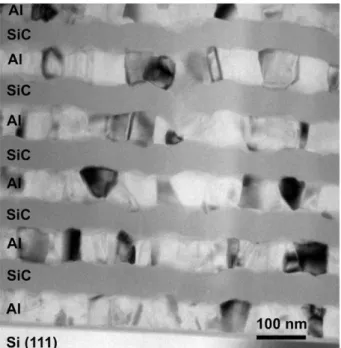
Fig. 1 shows a high-magnification cross-sectional bright-field (BF ) T E M image of the as-processed Al/SiC nanola-minate near the Si (111) substrate. The individual layer thickness was 60 ± 2 n m for Al and 59 ± 3 n m for SiC. The SiC layers were amorphous, while the Al layers were nanocrystalline, with columnar grains whose width (paral-lel to the layers) is of the order of the layer thickness, i.e.,
Al >
SiC
Al
SiC
A
i
SiC
Al
SiC
Al
SiC
Al
Si (111)
Wb
I
t
1 0 0 n m 2
Fig. 1. T E M cross section image of the as-processed Al/SiC nanolaminate.
60-100 nm. The interfaces between Al and SiC were chem-ically abrupt, with no evidence of chemical reactions, but physically rough as a result of the competitive columnar grain growth process that takes place in each consecutive Al layer.
There was no clear lateral correlation between the roughness of consecutive interfaces. This is clearly visible in Fig. 1. The first layer deposited on the atomically smooth thermally grown S i 02 substrate layer was Al. It
is a crystalline layer formed by the nucleation of columnar grains that grow at different velocities, leading to a rough surface. The growth of these grains is stopped by the next SiC layer, which is amorphous and whose top surface rep-licates the roughness of the bottom interface. The next Al layer, which was nucleated on this amorphous and rough surface, developed a new surface roughness as a result of the nucleation and growth of new grains that was indepen-dent of the previous interface.
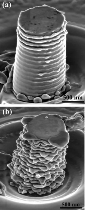
Two micropillars machined by F I B using annular mill-ing and lathe millmill-ing are shown in Fig. 2a and b, respec-tively. As expected, the pillars fabricated by annular milling showed a slight taper of ~2.5° on average, while the pillars fabricated by lathe milling showed virtually no taper.
Fig. 2. SEM Pictures of Al/SiC nanoscale multilayer micropillars fabri-cated by (a) annular milling, with slight taper (~2°) a n d (b) lathe milling without taper.
The initial loading slope of the stress-strain curves at 23 °C and 100 °C was much more compliant than that expected f r o m purely elastic loading. This behavior was attributed to the local plastic yielding at the top of the micropillar, because of slight misalignments between the micropillar surface and the flat punch, before full contact is established between the two [37]. This effect is clearly seen in the variation in elastic modulus of the micropillar, determined f r o m the slope of the unloading steps during the test, as a function of the applied displacement (Fig. 4). The elastic modulus increases until the applied dis-placement has reached 50-100 n m and full contact is estab-lished between the top of the pillar and the flat punch, leading to a constant value, independent of the applied dis-placement (Table 1).
0.12
Fig. 3. Compression stress-strain curves at 23 °C a n d 100 °C. The colors in the curves at 100 °C indicate that the tests were carried out either under displacement control (red) or load control (blue). ( F o r interpretation of the references to color in this figure legend, the reader is referred to the web version of this article. )
Table 1
Elastic modulus E, flow stress at 8% plastic strain oy. a n d H/of ratio of Al/ SiC nanoscale multilayers as function of temperature; hardness H was measured in Ref. [15] a n d is f o u n d in Table 2.
T= 23 °C T= 100 °C
E (GPa) <jf ( G P a ) Hhf E (GPa) <jf ( G P a ) 123 ± 2 3.1 ± 0 . 2 1.6 111 ± 3 1.6 ± 0 . 2 2.3
140
120
100 Q-CD
3 80
o E 60
o 40
20
• •
• 23°C b 1oo°c
50 100 150
Displacement (nm)
200 250
Table 2
Hardness H and elastic modulus E measured from instrumented nano-indentation tests in monolithic Al and SiC layers and Al/SiC nanoscale multilayers [15].
Materials T= 23 °C T= 100 °C
E (GPa) H (GPa) E (GPa) / / ( G P a ) Al
SiC Al/SiC
88 ± 6 297 ± 7
128 ± 7
0.91 ± 0.04 35.6 ± 0 . 7 4.9 ± 0 . 5
70 ± 3 320 ± 3 118 ± 11
0.60 ± 0.02 30.8 ± 0.8 3.7 ± 0 . 4
The theoretical transverse elastic modulus of the Al/SiC multilayer, E, can be computed from laminate theory according to
where Vai and FSic stand for the volume fraction of Al and
SiC (50% in this case), and EM and £"sic are the
corre-sponding elastic moduli. They were determined from instrumented nanoindentation tests in the monolithic films at 23 °C and 100 °C [15], as shown in Table 2. The theoret-ical values of transverse modulus according to Eq. (2) were 135 GPa and 114GPa at 23 °C and 100 °C, respectively, which are very close to the experimental values in Table 1. Interestingly , the elastic modulus of the Al/SiC multilay-ers determined from micropillar compression tests were similar, albeit slightly lower, than those determined from instrumented nanoindentation, shown in Table 2. The dif-ference, although very small, is very probably caused by the elastic anisotropy of Al/SiC laminates due to the layer ori-entation, as discussed in Ref. [2], While the transverse elas-tic modulus is measured directly during micropillar compression, nanoindentation tests perpendicular to the layers are influenced by both the transverse and the longi-tudinal elastic moduli, because of the multiaxial stress state. Thus, when loading perpendicular to the layers, in nanoindentation one would expect a slightly higher modu-lus because of the contribution from loading parallel to the layers.
While elastic moduli at 23 °C and 100 °C were very sim-ilar, as expected, the differences in plastic behavior were dramatic, considering the small variation in temperature. The micropillars tested at 23 °C presented a very high strain hardening rate, reaching 3.1 GPa at 8% applied strain, while the micropillars tested at 100 °C displayed a much softer behavior, and the flow stress seemed to satu-rate at 1.6 GPa when the applied strain reached ~ 8 %
(Fig. 3). It is worth noting that these marked differences
in the strain hardening capacity and in the flow stress were triggered by small changes in the homologous temperature
T/Tm from 0.3 (23 °C) to 0.4 (100 °C) in Al.
Nanoindentation experiments in monolithic films of both materials showed no variation in the properties of SiC between 23 °C and 100 °C, while the hardness of Al dropped by 30%, from 910 MPa to 600 MPa (Table 2).
These hardness values cannot be extrapolated directly to
the properties of the Al layers within the nanoscale multi-layer, because the thickness of the monolithic Al film was
1 (im, while the Al layers within the multilayer were only 60 nm thick. In this temperature range, the hardness of Al/SiC multilayers was also reduced by ~30%, the same percentage as that in the monolithic Al coatings (Table 2).
3.2. SEM and TEM observation of the deformed pillars
The compressed micropillars were studied by SEM to get a better understanding of the mechanisms of deforma-tion as a funcdeforma-tion of temperature. The micrographs corre-sponding to two micropillars deformed up to a plastic strain of 8% at 23 °C and 100 °C are shown in Fig. 5a
and b, respectively. The differences are obvious and corre-spond well to the differences in the stress-strain curve. The micropillars deformed at 23 °C showed evidence that the plastic deformation of the Al layers was constrained by the elastic SiC layers. Limited extrusion of the Al layers at the edges of the pillar was observed, especially towards the top, where the stresses are expected to be larger. In con-trast, Al was flowing out of the multilayer structure in the form of "tongues" at 100 °C, and this behavior can be a result of either a large reduction in the flow stress of the nanocrystalline Al, compared with the behavior at 23 °C, or of a substantial difference in the constraint imposed by the SiC layers.
TEM analysis of the deformed pillars, made by extract-ing thin foils through the center of the pillar usextract-ing FIB, provided additional information about the different defor-mation micromechanisms. A BF image of the full pillar deformed at room temperature up to 8% strain is depicted
in Fig. 6c. It shows that the plastic strain of the nanoscale
multilayer was accommodated by the plastic deformation of the Al layers. The strain was homogeneously distributed along the different Al layers, except for the Al layer just at the micropillar base, which showed extensive plastic defor-mation because of the stress concentration in this area. As a result of plastic deformation, the Al grains were slightly elongated perpendicular to the compression axis compared with as-deposited grains (Fig. 1), and some Al was extruded out at the free surfaces. The Al extrusion was more predominant towards the top of the pillar, where the stresses were higher as a result of the slight taper of this particular pillar, as can be seen in Fig. 6b. This image also shows one grain (see arrow) that has been extruded out of the multilayer, indicating that interface sliding was also present during deformation. This result is in agreement with the lack of chemical bonding between Al and amor-phous SiC, which should be able to accommodate sliding. It should be noted, however, that extrusion of Al at 23 °C was limited, and most of the Al layers did not extrude out in the pillar deformed at room temperature, as shown in Fig. 6c.
Fig. 5. SEM micrograph of Al/SiC nanoscale multilayer micropillar deformed up to a plastic strain of 8% at (a) 23 °C and (b) 100 °C.
matter of fact, no dislocations could be found in the deformed A1 layers, except for some dislocation pile-ups at the free surface of some layers, as pointed out by the white arrow in Fig. 6c. It is interesting to note that the only evidence of any dislocations was in these
areas of no constraint from the brittle SiC layers. This is consistent with the work of Sun et al. [38], who showed no dislocations after indentation of Al/SiC nan-olaminates at room temperature. It is possible that some dislocations could be annihilated at the numerous grain boundaries and Al/SiC interfaces after slip, although this does not explain the complete absence of dislocations in the Al layers. One can hypothesize that the fine grain size of the Al layers and the large degree of interfacial area would be conducive to interfacial and/or grain boundary diffusion at this temperature, contributing to a large degree of plastic flow in the Al layers.
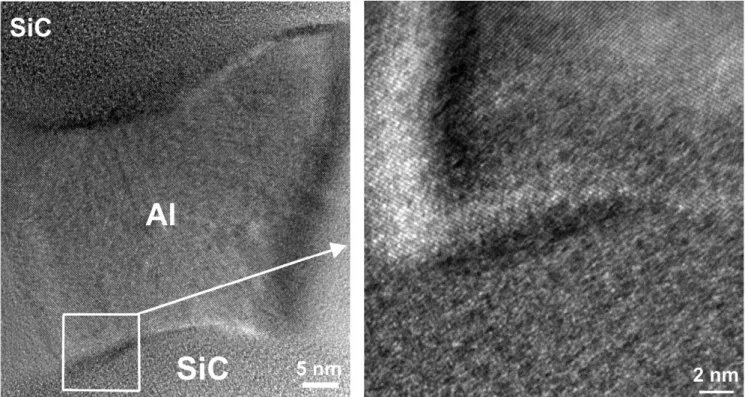
The pillar deformed at 100 °C showed widespread extrusion of the Al layers at the free surfaces along the micropillar (Fig. 7). Plastic deformation was also homo-geneously distributed along all the Al layers, except for the bottom layer, which underwent more extensive plastic deformation. No dislocations were found at 100 °C either, but Al grain extrusion was prevalent along the surfaces of the micropillar, indicating that interface slid-ing was dominant at 100 °C, compared with the behavior at 23 °C. It is important to point out that this change in the interface sliding behavior was not because of any chemical reactions at the Al/SiC interface. The interfaces between the crystalline Al and the amorphous SiC layers remained clean of any reaction products after testing at 100 °C, as shown in the high resolution TEM image in
Fig. 8.
In summary, micropillar compression tests of the nano-scale Al/SiC multilayers showed a dramatic reduction in the strain hardening rate and in the flow stress from 23 °C to 100 °C, while the nanoindentation hardness was only reduced by 30% in this temperature range. It is obvi-ous that the temperature increase will lead to some soften-ing of the nanocrystalline Al layers, as shown by the nanoindentation experiments performed in monolithic Al thin films (Table 2), but this mechanism cannot explain the reduction in the strain hardening rate nor the variation in the indentation constraint factor H/of from ~ 1.6 at 23 °C to - 2 . 3 at 100 °C (Table 1).
SEM and TEM analyses confirmed that the deforma-tion of the Al/SiC micropillars was controlled by the plastic deformation of the nanocrystalline Al layers con-strained by the elastic amorphous SiC layers. The TEM studies did not provide any evidence of dislocations in the Al layers. T E M analysis also demonstrated that interface sliding was limited at 23 °C and important at
(b)
1
J
r
i
«
*
X l
ff/.j
50 nm
(c)
I
1
1
r
h
*
a
50 nm
1
r
h
*
a
50 nm
Fig. 6. T E M images of Al/SiC micropillar deformed up to 8% at 23 °C: (a) region of the micropillar.
view; (b) detail of upper region of the micropillar; (c) detail of the lower
Fig. 8. High magnification T E M image of the Al/SiC interface after micropillar compression at 100 °C down to ! products.
i plastic strain, showing no reaction
4. Numerical model
4.1. Geometrical model
Numerical simulations of the micropillar compression test of Al/SiC nanoscale multilayers were performed using the Abaqus commercial finite element software [39]. The simulations were not aimed at predicting the stress-strain behavior, but at elucidating the influence of the flow stress of the Al layers and of the Al/SiC interface properties on the overall mechanical behavior of the micropillars under compression. The geometrical model of the micropillar compression test as well as the boundary conditions are depicted in Fig. 9. It consists of a cylindrical pillar with length 2 (im and radius 0.5 (_im (the dimensions of the experimental micropillars) and a circular flat punch. The pillar was composed of 30 layers of Al and SiC with iden-tical thicknesses. The bottom of the pillar was bonded to a semi-infinite elastic homogeneous medium with the effec-tive properties of the Al/SiC nanolaminate, to simulate accurately the testing conditions. The dimensions of the semi-infinite medium were large enough to avoid any effect of the boundary conditions on the simulated load-displace-ment curves. The flat punch was modeled as a rigid body, assuming frictionless contact between the micropillar and the flat punch.
Taking advantage of the axial symmetry, the model was meshed using two-dimensional four-node linear axisym-metric elements with reduced integration (CAX4R): 3600 elements were used to mesh the pillar and 14,440 elements for the semi-infinite medium. The mesh was refined at the
Load
6b
Fig. 9. Axisymmetric finite element model of micropillar compression composed of 15 bilayers of Al/SiC with a total height of 2 |xm and 1 |xm in diameter.
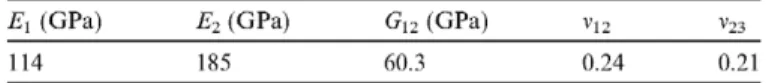
Table 3
Elastic constants of the transversally isotropic homogenized medium: direction 1 is perpendicular to the isotropy plane 23.
Ei (GPa) E2 (GPa) G12 (GPa) v12 v23
114 185 60.3 0.24 0.21
Fig. 10. Constitutive equation for the cohesive interface crack under mixed-mode loading.
4.2. Material properties
The model included three different bulk materials, namely SiC, Al and the homogenized nanolaminate, and the Al/SiC interface. The SiC layers were modeled as elastic isotropic solids with an elastic modulus of 300 GPa and a Poisson's ratio of 0.14. The Al layers were modeled as elas-toplastic, isotropic solid following the Von Mises yield cri-terion. The elastic modulus and Poisson's ratio were, respectively, 70 GPa and 0.34. It was assumed that the strain hardening capacity of the Al layers was negligible because of their nanocrystalline structure and the small layer thickness. The homogenized elastic medium at the base of the pillar was assumed to be transversally isotropic, and the five independent elastic constants, estimated from laminate theory, are found Table 3 [40,41].
To account for the effect of interface sliding, which according to the T E M observations of Fig. 7 take place at 100 °C, the Al-SiC interface was modeled phenomeno-logically as a cohesive crack. In this model, the total stress acting on the interface, t = J(t„)2 + t2s, is related to the
corresponding displacement jump 3 = J (3n)2 + S2s, where
tn and ts stand for, respectively, the normal and shear
stres-ses transferred through the cohesive crack, while 3n and 8S
are the corresponding normal and shear displacement jumps across the cohesive interface. The ( ) symbol stands
for the Macaulay brackets, which returns the argument, if positive, and zero otherwise, because compressive normal stresses do not open the crack. The simplest constitutive equation for the cohesive crack is the bilinear model
(Fig. 10). In the absence of damage, the interface behavior
is linear with an initial stiffness iT(1012 GPa m- 1'), which is
a numerical parameter large enough to ensure the displace-ment continuity at the interface and to avoid any modifica-tion of the stress fields in the absence of damage. The onset of damage is attained when the total stress acting on the interface reaches a critical value f given by a quadratic cri-terion according to
where fn and fs stand for, respectively, the normal and shear
interface strength [42]. In the case of the micropillar com-pression test, the normal stresses are always compressive and thus (tn) = 0 and the actual value of fn is not relevant.
Shear stresses parallel to the interface developed as a result of the mismatch in the mechanical properties of the Al and SiC layers, and interface damage occurred when
ts = tCs = f .
Once damage begins, the stress transferred through the interface and the interface stiffness are reduced, depending on the interface damage parameter d, which evolves from 0 (in the absence of damage) to 1 (no stresses transmitted across the interface). The evolution of cl is controlled by the displacement jump across the interface, 8, the total stress acting at the interface at the onset of damage, f , and the interface fracture toughness T = 0.5 • f • & (the area under the curve), which is independent of the loading path in this model. Once the cohesive crack is completely broken, interface sliding is opposed by Columbian friction with a friction coefficient \.i, which, together with the inter-face shear strength fs, and the interface toughness T,
deter-mines the interface properties. More details about the cohesive crack model can be found elsewhere [3,34,43,44].
4.3. Numerical results
A parametric study was carried out using the model outlined above to ascertain the influence of the Al yield stress <rv (in the
range 50-1000 MPa), and of the interface shear strength f
(between 0 and 1 GPa) and friction coefficient \.i (in the range 0-0.3) on the compressive stress-strain curve of the nanoscale multilayer. As mentioned above, nanocrystalline Al was assumed to have a negligible strain hardening capacity. More-over, interface toughness was set to T — 100 J m 2 in all cases,
in agreement with the available experimental data for this type of metal-ceramic interfaces [45].
The compressive stress-strain curves as a function of the Al yield stress av are plotted in Fig. 1 la in the case of a
01 CL e>
CO
|(b)'
c 1t (MPa)
• Perfect interface
0.02 0.04 0.06
Strain 0.02 0.04 0.06 0.08 0.1
Strain
ro CL O
CO
Fig. 11. Simulation results. Effect of: (a) the Al yield stress <jv for the case of a perfect interface; (b) the interface strength f for <jv = 350 M P a a n d /i = 0; (c) the interface friction /i for <rv = 450 M P a a n d f = 0 M P a .
SiC layers on the plastic deformation of Al. Constraint leads to the development of high compressive hydrostatic stresses, increasing the uniaxial applied stress required for yielding. This is shown in Fig. 12a, in which the contour plots of hydrostatic pressure are plotted as a function of the applied strain for the multilayer with av — 350 MPa.
They increased rapidly in the Al layers during the elasto-plastic transition (from 1.5% to 7.5% applied strain) and were maximum in the centre of the pillar. They were relieved at the free edges as a result of the extrusion of the Al out of the pillar, which took place in the absence of interface sliding.
The effect of the interface strength f on the compressive stress-strain curve is depicted in Fig. l i b , assuming a matrix yield strength of 350 MPa and a frictionless inter-face after fracture. Although the frictionless hypothesis is not realistic, it is useful to understand independently the
effects of interface strength and friction. The curves are superposed until the shear stresses at the interface over-come the interface strength leading to free interface sliding in the absence of friction. As a result, no hydrostatic stres-ses were built up in the Al layers during deformation after interface fracture, and the strain hardening capability of the multilayers disappeared beyond this point. Thus, the multilayer strength depended on the interface shear strength, which determined the critical strain for interface fracture. The influence of the elastic constraint on the mechanical behaviour is readily appreciated in Fig. l i b if the curves of multilayers with different interface strengths are compared with that of the material with a perfect inter-face. In the limit of a very weak ( f — 0) frictionless (/< = 0) interface, the constraint of the SiC layers was negligible
(Fig. 12b), and the Al/SiC micropillar would yield at the
(GPa)
c = 7.5% e = 15%
(GPa)
(b)
e = 1.5% e = 15%
Fig. 12. Contour plots of hydrostatic pressure as a function of the applied strain for nanoscale multilayers with (a) perfect interface; (b) weak frictionless interface ( f = 0 and /i = 0).
Finally, the effect of the interface friction of the mechan-ical response is shown in Fig. 11c for a Al/SiC multilayer with an Al yield strength of 450 MPa and a weak interface (?c = 0). Even though the interface strength is negligible,
the constraint imposed by frictional stresses on interface sliding leads to the build-up of hydrostatic stresses and to the development of strain hardening in the multilayer. It is worth noting that a friction coefficient >0.25 induces a constraint equivalent to that of a perfect interface.
4.4. Correlation between experiments and simulations
The simulations above demonstrated that the compres-sive behavior of Al/SiC micropillars was controlled both by the yield stress of the Al layers (oy) and the interface properties ( f , /()• Assuming a reasonable value of the inter-face friction coefficient (/< = 0.1-0.3), the simulations also showed that the interface strength is not a critical parame-ter, since, even for a very weak interface, sliding will be dominated by frictional forces. Interface sliding affects the constraint imposed by the SiC layers, which in turn determines the ratio of compressive strain required for plastic flow of the Al/SiC micropillar with respect to the Al yield stress, which ranges between 1 for a frictionless weak interface and 5 for a perfect interface. So, in modify-ing the interface properties, only the frictional coefficient will be taken into account.
Therefore, in order to correlate the simulated and exper-imental curves, the Al yield stress and the friction coeffi-cient have to be chosen as functions of temperature. The experimental curves of Fig. 3 clearly show that the strain hardening rate at 23 °C was much more pronounced than at 100 °C, indicating different levels of constraint and thus differences in the amount of interface sliding during defor-mation. This conclusion is supported by the limited inter-face sliding observed at 23 °C by T E M (Fig. 6), as opposed to the behavior found at 100 °C (Fig. 7). Based on this information, and assuming a perfect interface at 23 °C (no sliding), a good correlation between experimental results and simulations at 23 °C could be obtained for <rv = 650 MPa, as shown in Fig. 13a, which also depicts
simulation results for different friction coefficients (0.3 and 0).1 This value of the Al yield strength is reasonable
for an Al layer 60 nm thick, considering that the yield stress of an Al thin film 1 (im thick deposited in the same condi-tions should be of the order of 340 MPa, as estimated from its hardness of 910 MPa (Table 2) and using H « 2.7<rv.
Regarding the results at 100 °C, it is difficult to provide an accurate estimation of yield strength of the Al layers at this temperature. Assuming a perfect interface, the experi-mental results were well fitted with <rv = 350 MPa, which
would imply a reduction of —50% with respect to the room temperature yield stress (Fig. 13b). The experimental T E M observations of extended interface sliding at 100 °C
(Fig. 7), however, favored the selection of an interface
fric-tion — 0.2 in combinafric-tion with <rv = 450 MPa. This
choice led to a very good fit of the experimental data and
3.5
3
2.5
0
1
1 5 051
0.5
0 0 0.02 0.04 0.06 0.08 0.1 0.12 0.14
Strain
3.5
3
2.5
CD u> S 1.5 c/5
1
0.5
0 0 0.02 0.04 0.06 0.08 0.1 0.12 0.14
Strain
Fig. 13. C o m p a r i s o n between experimental a n d numerical compressive stress-strain curves at (a) 23 °C a n d (b) 100 °C. In (a), the yield stress of Al was set to 650 M P a . while the interface properties were varied considering either a perfect interface or a weak interface ( f = 0) with a friction coefficient /i of 0 or 0.3. In (b). the yield stress of Al was set to 350 M P a a n d a perfect interface or to 450 M P a with a weak interface ( f = 0) a n d interface friction /i in the range 0-0.2.
was compatible with the extended interface sliding observed experimentally. Moreover, it is interesting to note that the reduction in the yield stress of the Al layers of ^ 3 0 % at 100 °C is equivalent to the reduction in hardness determined for Al thin films 1 (im thick, although this should not necessarily be the case for Al films of different thicknesses and thus different grain sizes (Table 2). All in all, the large reduction in the flow stress and the strain hardening rate of Al/SiC nanoscale multilayers f r o m 23 °C to 100 °C can be explained by a combination of two mechanisms: the d r o p in the yield stress of nanocrys-talline Al together with easier interface sliding at the Al/ SiC interfaces. This is likely to occur in nanocrystalline Al as a result of the increased activation of dislocation
climb and/or interface diffusion, as the homologous tem-perature is raised f r o m 0.3 to 0.4.
Finally, it is worth noting that this combination of changes in yield stress and interface friction can explain the discrepancy between the H/of ratios between 23 °C and 100 °C. (Table 1). The simulations showed that inter-face sliding was a controlling mechanism during micropil-lar compression and that Al was extruded out of the pillar because of the lack of constraint in the lateral sur-faces. However, Al plastic flow during nanoindentation was constrained vertically by the SiC layers and laterally by the surrounding undeformed material. Therefore, inter-face sliding was not permitted, regardless of the interinter-face strength and friction coefficient and, as a result, the hard-ness of Al/SiC at 100 °C was reduced by the same amount as the Al yield stress, i.e., ~30%. The flow stress during micropillar compression was reduced, however, by ~ 5 0 % because of the additional effect of interface sliding leading to the unconstrained extrusion of Al at the free micropillar surfaces.
5. Conclusions
Micropillar compressions tests were carried out to ascer-tain the influence of temperature (between 23 °C and
100 °C) on the mechanical properties of Al/SiC nanoscale multilayers. The multilayers (composed of alternating lay-ers 60 n m thick of nanocrystalline Al and amorphous SiC) presented a very high strain hardening rate at 23 °C, leading to a flow stress of 3.1 ± 0.2 G P a at 8% strain. How-ever, the hardening rate decreased dramatically at 100 °C, and the flow stress at 8% strain was reduced to 1.6 ± 0 . 2 GPa. SEM and T E M observations of the deformed pillars showed that homogeneous plastic defor-mation of the Al layers controlled the mechanical behavior. However, Al plastic deformation was constrained by the SiC layers at 23 °C while massive extrusion of the Al out of the pillars was observed at 100 °C. Flow of the Al layers may have been facilitated by interfacial diffusion, since no dislocations were observed in the Al layers.
Finite element simulations of the micropillar compres-sion tests were performed to explain the role of Al flow stress and interface properties (strength and friction coeffi-cient) on the compressive stress-strain curve. Very high hardening rates were obtained, assuming a perfect interface between Al and SiC as a result of the hydrostatic stresses generated by the elastic constraint of the SiC layers on the Al plastic flow. The simulated stress-strain curves assuming perfect bonding at the interface were in good agreement with the experimental data at 23 °C for reason-able values of the Al yield strength. If interface sliding was allowed, the hardening rate was determined by the friction coefficient between Al and SiC, which controlled the extru-sion of the Al out of the micropillar by the lateral surfaces. Numerical simulations indicated that a reduction in both the Al yield strength and the constraint by interfacial slid-ing were necessary to explain the experimental results, in
Experiments
— a = 350 MPa, perfect interface
y
- • - a =450 MPa, 11 = 0.2
y
- a - a =450 MPa, n = 0.1
y
- a = 450 MPa, jj = 0.0
agreement with the experimental observations at 100 °C. Finally, it should be noted that these differences were not detected using nanoindentation to determine the mechani-cal properties of the multilayer, because lateral flow of Al is always constrained by the surrounding undeformed mate-rial. Thus, micropillar compression tests emerge as a criti-cal tool for characterizing the mechanicriti-cal performance of nanoscale multilayers with limited interface strength.
Acknowledgements
This investigation was supported by the National Sci-ence Foundation of the U S and the Spanish Ministry of Economy and Competitiveness under the Materials World Network Program through the "High temperature mechanical behavior of metal/ceramic nanolaminate com-posites" project. Additional support f r o m the European Commission through the R A D I N T E R F A C E S project (Grant Agreement Number 263273) is also gratefully acknowledged.
References
[1] Mara N . Sergueeva A. Misra A. Mukherjee AK. Scr Mater 2004:50:803.
[2] Deng X. Chawla N . Chawla K K . K o o p m a n M. Chu JP. Adv Eng Mater 2005:7:1099.
[3] Wu T-H. Cheng C-R. Lee J-K. Tsai S-Y. Peng J-H. US patent 08237235: 2010.
[4] Chance DA. Wilcox DL. Proc IEEE 1971:59:1455.
[5] Jimenez-Villacorta F. Espinosa A. Cespedes E. Prieto C. J Appl Phys 2011:110:113909.
[6] Garcia-Garcia A. Vovk A. Pardo JA. Strichovanec P. Magen C. Snoeck E. et al. J Appl Phys 2009:105:063909.
[7] Lenoble O. Bauer P. Bobo JF. Fischer H. Ravet M F . Piecuch M. J Phys: Condens Matter 1994:6:3337.
[8] Nunes C. Teixeira V. Prates M L . Barradas NP. Sequeira AD. Thin Solid Films 2003:442:173.
[9] Zhang Q-C. J Phys D: Appl Phys 2001:34:3113.
[10] Zhao S. Wackelgard E. Sol Energy Mater Sol Cells 2006:90:243.
[11] PalDey S. Deevi SC. Mater Sci Eng: A 2003:342:58.
[12] Holleck H . Schier V. Surf Coat Technol 1995:76-77(1):328. Part 1.
[13] Hennings D F K . In: Proceedings of the 2000 12th IEEE international symposium, vol. 1: 2000. p. 135.
[14] Kishi H. Mizuno Y. Chazono H. Jpn J Appl Phys 2003:42:1.
[15] Lotfian S. Molina-Aldareguia JM. Yazzie KE. Llorca J. Chawla N. Philos Mag Lett 2012:92:362.
[16] Rodriguez M. Molina-Aldareguia JM. Gonzalez C. Llorca J. Acta Mater 2012:60:3953.
[17] Cheng Y-T. Cheng C-M. Mater Sci Eng R: Reports 2004:44:91.
[18] D a o M. Chollacoop N . Van Vliet KJ. Venkatesh TA. Suresh S. Acta Mater 2001:49:3899.
[19] Chawla N . Singh D . Shen YL. Tang G . Chawla K. J Mater Sci 2008:43:4383.
[20] Shen Y-L. Tang G. Int J Mater Struct Integr 2009:3:102.
[21] Tang G. Singh D R P . Shen YL. Chawla N . Mater Sci Eng: A 2009:502:79.
[22] Carpenter JS. Misra A. Uchic M D . Anderson PM. Appl Phys Lett 2012:101:051901.
[23] M a KJ. Bloyce A. Bell T. Surf Coat Technol 1995:76-77:297. Part 1.
[24] Kunz A. Pathak S. Greer JR. Acta Mater 2011:59:4416.
[25] Uchic M D . Dimiduk D M . Mater Sci Eng: A 2005:400^101:268.
[26] Greer JR. Oliver WC. Nix WD. Acta Mater 2005:53:1821.
[27] Uchic M D . Dimiduk D M . Florando JN. Nix W D . Science 2004:305:986.
[28] Soler R. Molina-Aldareguia JM. Segurado J. Llorca J. Merino RI. Orera VM. Int J Plasticity 2012:36:50.
[29] Korte S. Clegg WJ. Scr Mater 2009:60:807.
[30] Song SX. Lai Y H . Huang JC. Nieh TG. Appl Phys Lett 2009:94:061911.
[31] Deng X. Cleveland C. Chawla N . Karcher T. K o o p m a n M. Chawla K. J Mater Eng Perform 2005:14:417.
[32] Singh D R P . Chawla N . Tang G. Shen YL. Acta Mater 2010:58:6628.
[33] Bei H. Shim S. Miller M K . Pharr G M . George EP. Appl Phys Lett 2007:91:111915.
[34] Motz C. Schoberl T. Pippan R. Acta Mater 2005:53:4269.
[35] Sneddon IN. Int J Eng Sci 1965:3:47.
[36] Greer JR. Nix WD. Appl Phys A: Mater Sci Process 2005:80:1625.
[37] Soler R. Molina-Aldareguia JM. Segurado J. Llorca J. Adv Eng Mater 2012:14:1004.
[38] Sun PL. Chu JP. Lin TY. Shen YL. Chawla N. Mater Sci Eng: A 2010:527:2985.
[39] Hibbit. Karlsson. Sorensen. Abaqus. Abaqus User's manual 2011. [40] Dehm G. Prog Mater Sci 2009:54:664.
[41] Snead LL. Nozawa T. Katoh Y. Byun T-S. Kondo S. Petti DA. J Nucl Mater 2007:371:329.
[42] Williams JJ. Segurado J. Llorca J. Chawla N. Mater Sci Eng: A 2012:557:113.
[43] Canal LP. Gonzalez C. Segurado J. Llorca J. Compos Sci Technol 2012:72:1223.
[44] Canal LP. Segurado J. Llorca J. Int J Solids Struct 2009:46:2265.
[45] Dalgleish BJ. Trumble KP. Evans AG. Acta Metall Mater 1989:37:1923.