Impact of Metal-Organic Vapor Phase Epitaxy Environment on
Silicon Bulk lifetime for III-V-on-Si Multijunction Solar Cells
Elisa García-Tabarés , Ignacio Rey-Stolle
ABSTRACT
With the final goal of integrating III-V materials on silicon substrates for tandem solar cells, the influence of the Metal-Organic Vapor Phase Epitaxy (MOVPE) environment on the minority carrier properties of silicon wafers has been evaluated. These properties will essentially determine the photovoltaic performance of the bottom cell in a III-V-on-Si tandem solar cell. A comparison of the base minority carrier lifetimes obtained for different thermal processes carried out in a MOVPE reactor on Czochralski silicon wafers has been carried out. An important degradation of minority carrier lifetime during the surface preparation (i.e. H2 anneal) has been observed. Three different mechanisms have been proposed for explaining this behavior: 1) the introduction of extrinsic impurities coming from the reactor; 2) the activation of intrinsic lifetime killing impurities coming from the wafer itself; and finally, 3) the formation of crystal defects, which eventually become recombination centers. The effect of the emitter formation by phosphorus diffusion has also been evaluated. In this sense, it has been reported that lifetime can be recovered during the emitter formation either by the effect of the P on extracting impurities, or by the role of the atomic hydrogen on passivating the defects.
1. INTRODUCTION
Multijunction solar cells (MJSCs) are one of the most successful device architectures to implement ultra high efficiency photovoltaic devices. More specifically, the combination of III-V compounds and silicon (Si) in hybrid MJSCs represents a long sought for device that would link the already demonstrated efficiency potential of III-V semiconductor MJSCs with the low cost and unconstrained availability of silicon substrates. The ultimate goal is to produce high-efficiency photovoltaic devices, while reducing the cost of solar electricity down to levels competitive with conventional sources.
carrier parameters will determine the PV performance of the bottom sub-cell in the tandem stack [13]. It is well established that the minority carrier lifetime in conventional PV silicon processing is not a constant material property but depends strongly on the thermal history and the environment where the sample was processed [14]. Analogously, a strong influence of the metal-organic vapor phase epitaxy (MOVPE) environment on this parameter has been reported by us elsewhere [15].
In this paper we will present results about minority carrier lifetime evolution in the MOVPE processing of silicon substrates for III/V-on-Si photovoltaics. Essentially two alternatives have been proposed in the literature for this processing or, more in particular, for the formation of the silicon subcell emitter. The first one is based on the homoepitaxial growth of silicon on the Si substrate [3,6]. This implies either the need for a special MOVPE reactor able to grow both group IV and III-V compounds (i.e. specially designed to minimize cross-contamination and carry over effects), or to grow the structure in a two-step process (i.e. taking the samples out of the reactor after Si growth, cleaning the reactor, and loading again for III-V growth). The use of homoepitaxial growth of Si has demonstrated to be a beneficial factor in the production of high quality GaP-on-Si layers [3,6], though, as discussed, introduces an additional degree of complexity in the epitaxial process. A simpler alternative would be to mimic what is done in conventional MJSC technology on germanium substrates, where the bottom subcell emitter is formed by diffusion of phosphorous (P), resulting from the pyrolysis of phosphine (PH3). In this respect, it should be noted that several groups have also reported high quality GaP layers without homoepitaxial silicon buffers [2, 9]. Accordingly, in this work we will focus on this strategy and consider the formation of the emitter from diffusion as is the case in conventional III-V triple-junction solar cells based on germanium.
under phosphine (PH3) to enable the diffusion of phosphorus (P) into the silicon substrate [18]; and 3) finally, as a result of the surface degradation caused by the PH3 exposure during the formation of the emitter, substrates need to be submitted to an additional treatment, aimed to recover the surface morphology for subsequent epitaxial growth [19]. In this sense, the formation of the emitter by exposing wafers to a high PH3 concentration is followed by a H2 annealing intended to recover the damaged surface morphology. Therefore, the impact on the base minority carrier lifetime of these three processes and environments will be assessed in this paper.
2. EXPERIMENTAL
layer) and then were passivated using the above mentioned wet method. Minority carrier lifetime was measured on the wafers using the well-known Photoconductance Decay (PCD) technique.
3. RESULTS
3.1 Impact of surface preparation
The effect of the surface preparation (i.e. high temperature annealing under H2) on the minority carrier lifetime was studied elsewhere [15]. Results are summarized in fig. 1.
Fig. 1. Minority carrier lifetime for wafers annealed at 830ºC and 900 mbar of H2 for different times. An
as-received wafer was included for comparison. Lifetime values were calculated for an injection level of 1014 cm-3 (except for the as received wafer, which was measured for 1015 cm-3).
wafer surface, which diffuses into the bulk at high temperatures (either present in the as-received wafer and not removed in the cleaning or introduced by the MOVPE environment); c) the activation (i.e. unpassivation) of lifetime killing centers in the Si bulk (initially non-active in the bulk); and finally d) the formation of crystal defects which eventually become recombination centers. The light induced degradation, enhanced by the activation of B-O pairs, was eventually discarded, since the same results were observed when working with gallium-doped silicon wafers, were Boron is not present [15]. The other possibilities have been studied in this work.
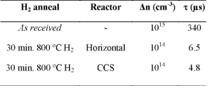
First of all, in order to fully rule out this degradation is a particular effect, caused by certain contamination present in our horizontal reactor; some of the experiments were repeated in a different reactor (CCS MOVPE). Results are presented in table 1.
Table 1. Minority carrier lifetime for wafers annealed in hydrogen for 30 min. at 100 mbar in two different reactors.
H2 anneal Reactor An (cm3) T (µs)
As received - 1015 340
30 min. 800 ºC H2 Horizontal 1014 6.5
30 min. 800 ºC H2 CCS 1014 4.8
As it is shown in table 1, the same results were obtained after the H2 anneal, regardless of the reactor
used for the thermal treatment. These results prove that the lifetime degradation observed after the
surface preparation at MOVPE is neither the effect of a particular reactor condition nor configuration.
On the contrary, lifetime degradation seems inherent to the MOVPE environment used for III-As/P
growth.
It is well know that any metal contaminants initially present on a wafer surface will diffuse into the
wafer’s bulk during a high temperature annealing, as a result of the thermal load. In this sense, the
importance of a thorough wafer cleaning before subsequent thermal processing has been repeatedly
behavior, the impact of the cleaning method on the minority carrier lifetime has been assessed (Table 2). With this aim, wafers were cleaned using different methods and afterwards, they were annealed following the same MOVPE routine (i.e. 30 min. hydrogen annealing at 830 ºC). Three different cleaning methods were tested: 1) Method A: diluted fluorhydric acid; 2) Method B: diluted fluorhydric acid followed by a de-ionized water rinse; 3) Method C: the standard RCA cleaning (NH4OH:H2O2:H2O 1:1:5 + HF:H2O 1:50 + HCl:H2O2:H2O 1:1:6 + HF:H2O 1:50). Furthermore, a non-cleaned wafer was included for comparison.
Table 2. Minority carrier lifetime of wafers cleaned following different routines. They were annealed in
hydrogen afterwards for 30 min at 100 mbar.
Cleaning None None Method A Method B Method C
H2 anneal
As-received
30 min. 830 ºC 30 min. 830 ºC 30 min. 830 ºC 30 min. 830 ºC
Δn (cm3)
1015 1014 1014 1014 1014 T(µs 340 8.9 7.5 5.9 5.4
As table 2 evidences, no significant difference was observed on minority carrier lifetime despite the fact that different cleaning methods were used.
Fz wafers is reported in table 3. Roughly the same degradation was measured after the H2 annealing
regardless the wafer growth method (table 3).
Table 3. Minority carrier lifetime comparison for Cz and Fz wafers annealed in H2 for 30 min.
Wafer nature H2 anneal Δn (cm3) T(µs)
Cz As-received 1015 340
Cz 30 min. 830ºC 1014 4.1
Fz As-received 1015 445
Fz 30 min. 830ºC 1014 5.0
Finally, it has been assessed whether the lifetime degradation is caused by the activation of impurities
coming from the reactor atmosphere. For conventional silicon PV technology, it has been reported,
that the presence of H2 in p-type crystalline Si wafers is not desirable because of the introduction of
lifetime killing centers by the formation of H-O related complexes [14, 22]. The behavior of Fz
wafers, were O is not present and which exhibited a lifetime degradation virtually identical to that of
Cz-silicon, made us rule out this possibility. However, in order to fully discard this option we
conducted an experiment aimed to confirm the effect of the carrier gas influence on to the lifetime
degradation. In this case, nitrogen was used as the carrier gas and therefore samples were thermally
treated in the absence of H2. Results of this experiment are summarized in Table 4 . As it is shown in
Table 4, loosely the same values were measured after the annealing disregarding of the carrier gas,
suggesting that H2 carrier gas does not have a determinant role in the degradation of electron lifetime
in the p-silicon wafer. However, in a MOVPE environment Si wafers are treated in a chamber where
several group-III and group-V species coexist in the presence of organic radicals, hydrogen carrier
gas and high temperatures. Therefore, other species (apart from hydrogen) could be involved in this
Table 4. Minority carrier lifetime of wafers annealed for 30 min. at 900 mbar in different atmospheres. In this case, wafers have a lower resistivity (1-5 ohm·cm)
MOVPE treatment Δn (cm3) T (µs)
As-received 1015 107
30 min. 800 ºC H2 anneal 1015 14.5
30 min. 800 ºC N2 anneal 1015 17.2
3.2 Impact of the emitter formation
Fig. 2. Average minority carrier lifetime for Si wafers annealed under 32.1 mbar of PH3 at 800 ºC and 830 ºC for different times. Lifetimes were calculated for an injection level of 1015 cm-3.
The average lifetime has been plotted in Fig. 2, which shows the lifetime evolution as a function of the PH3 annealing conditions. The error bars represent the maximum and minimum values measured for each sample. The high variability of the results will be discussed in section 4.
3.3 Impact of anneals to recover surface morphology
on PH3 exposure (P diffusion) followed by a H2 annealing, lead us to obtain an optimum emitter (shallow and highly doped) while recovering surface morphology to acceptably low RMS roughness values [19].
The impact of this combined treatment on the minority carrier lifetime has been assessed. With this aim, a lifetime comparison between wafers annealed in PH3 (samples 1, 3 and 7) and wafers submitted to the combined treatment (as described in table 5) is presented in fig. 3.
Fig. 3. Minority carrier lifetime for samples summarized in table 5. Solid bars correspond to samples annealed
Table 5. Description of the third batch of experiments where wafers were first annealed under hydrogen mixed with 32.1 mbar of PH3 and then annealed under pure H2.
Sample
1 2 3 4 5 6 7 8
PH3 anneal (32.1 mbar)
30 min. 800 ºC
30 min. 830 ºC
10 min. 875 ºC
H2 anneal conditions
20 min. 830 ºC
20 min. 830 ºC 60 min. 830 ºC 60 min. 875 ºC
60 min. 875 ºC
4. DISCUSSION
The evolution of the minority carrier lifetime of Si wafers during different treatments aiming the optimization of the Si bottom subcell has been analyzed. First of all, we have studied the effect of the surface preparation (H2 anneal at 830 ºC) on the minority carrier lifetime. We have reported an unquestionable degradation in minority carrier lifetime as a result of the thermal treatment. It has been observed a rapid lifetime drop in the first minutes of the annealing and, afterwards, its progressive decrease until the lower detection limit of our PCD equipment is reached (~1 µs). In order to confirm the reproducibility of these results, some of the experiments were repeated in a different MOVPE reactor and the same effects were observed. Obviously, such low minority carrier lifetimes in the base of the silicon bottom subcell would make it impossible to manufacture even a modest-performing solar cell.
conventional silicon PV technology have been used for cleaning the wafers. The same results were obtained in all cases, regardless of the cleaning method, indicating that the wafer cleaning procedure is not the main factor impacting lifetime.
Another possibility which was considered for explaining this behavior is the activation of lifetime killing impurities during the MOVPE treatment, which might be present initially in the bulk in an inactive state. If this assumption is correct, using Fz wafers (which have a significantly lower impurity concentration, as compared to the Cz wafers), should show a higher immunity to lifetime degradation. On the contrary, the same behavior was observed regardless the wafer growth method and supplier. Hence, it seems unlikely that this phenomenon is responsible for the lifetime degradation, although we can’t fully discard this hypothesis.
One of the distinctive features of the MOVPE process is that it is developed under H2 carrier gas, which is a significant difference as compared to processing environments in conventional PV technology. According to the literature, the use of hydrogen at high temperatures might have a determining effect on reducing the lifetime by the introduction of deep-level defects associated to H-O pairs [14, 22]. In order to confirm this possibility, we have repeated some of the experiments using N2 as carrier gas but the same effects were observed. Hence, lifetime degradation cannot be attributed to H2 either. Furthermore, in a prior work [15] we also ruled out that the formation of B-O pairs –we use CZ-grown B-doped silicon wafers– was behind this degradation since Ga-doped silicon wafers exhibited the same lifetime degradation.
In summary, the reason for the lifetime degradation is still unknown and different experiments are undergoing to clarify it. However, this effect has been found to be linked to a MOVPE environment but unrelated to the use of H2 as the carrier gas, independent of the wafer nature, the cleaning procedure prior to loading the wafers in the reactor, and not caused by the formation of B-O pairs.
despite the initial degradation during the heating up of the wafer, lifetime can be recovered during the emitter formation, as it is shown in fig. 3. The impact on annealing duration and temperature are difficult to assess. In the worst cases, lifetime was recovered to the initial value of the as-received wafer; while in the best cases, values larger than 1ms were measured.
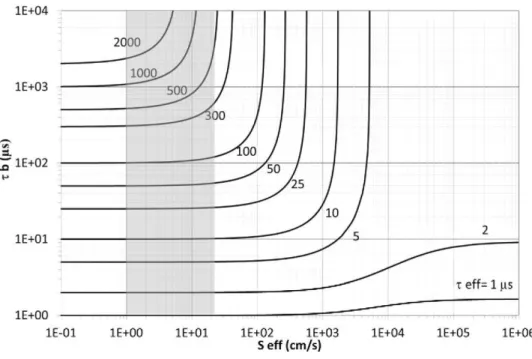
The wide range of variation of the minority carrier lifetimes measured in the experiments is believed to be related to the surface passivation quality. According to [23], the effective lifetime (xeff) is related with the bulk lifetime (xb) and the effective surface recombination velocity (Seff) as follows:
^ f y K7)1 (1)
Being D the diffusion coefficient for silicon (30 cm2/s) and W de wafer thickness (275 µm). This equation is valid for surface recombination velocity (Seff) lower than 107 cm/s.
According to eq. 1, the effective lifetime will be limited by the surface recombination velocity for samples with a very high bulk lifetime. On the contrary, it will be determined by the bulk lifetime for samples with an excellent passivation quality (i.e very low Seff). Fig. 4 shows the contribution of xb and Seff to the effective lifetime. It shows the importance of having a low surface recombination velocity for measuring high effective lifetimes.
are in the 10-50 cm/s range [25]. Finally, typical values of about 10 cm/s were usually measured for quinhydrone/methanol passivated Si surfaces (the strategy used in this paper); being the lowest Seff reported 4.2 cm/s for a Fz Si wafer [20]. Accordingly, it cannot be assumed a constant Seff for all the samples, since it will be deeply modulated by the surface preparation and the wafer properties; however it seems reasonable to expect a Seff in the range of 1-20 cm/s for our quinhydrone/methanol passivated surfaces (shown as a gray stripe in fig. 4).
Fig. 4. Effective lifetime for a 275 µm thick Si wafer as a function of bulk lifetime and surface recombination
velocity. A gray stripe, which corresponds to the expected range of Seff using quinhydrone methanol solution as the passivating agent, has been also included.
Seff) the surface recombination limits the effective lifetime, and hence, the gap between xb and Teff increases, measuring much lower xeff. This fact can thereby explain the big variability in measurements depicted in fig. 2. In this sense, for a wafer with a certain xb, only when a perfectly cleaned surface is obtained, an excellent passivation quality is achieved and thus, a xeff close to the xb is measured (highest level of the error bars included in fig. 2). On the contrary, when surfaces are not perfectly passivated (because of a poorer cleaning or non-uniform passivation) the Seff begins to limit the effective lifetime, measuring lower xeff (lowest level of the error bars in fig. 2) for the same xb.
With such wide variation ranges (which are the result of small changes in the processing of the samples) we have concluded that we cannot accurately and repeatedly determine lifetimes above 350 µs. In other words, for measured lifetimes below 350 µs, we can be sure that they are close to the real bulk lifetime. For measured lifetimes above the 350 µs limit, we are limited by surface recombination velocity and the effective lifetime is just a lower limit for the bulk lifetime.
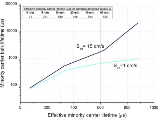
Fig. 5. Compassion of bulk lifetime, calculated from average effective lifetimes reported in fig. 2 for 800 ºC,
In summary, the effect of the PH3 annealing on recovering lifetime has been demonstrated. However, it is complicated to quantify this improvement, since results will be deeply affected by small (i.e. highly uncontrollable) changes in the surface passivation quality that will limit our precision to assess the real bulk lifetime.
Finally, we have reported the effect on the lifetime of a second annealing in pure H2 (intended to recover surface morphology) after P diffusion (see fig. 3). Although bulk lifetime reaches high values after PH3 exposure (solid bars in fig. 3), it gradually degrades after the second step in H2 (dashed bars). This degradation is deeply modulated by the H2 annealing conditions; becoming more important as the temperature and duration increase, as shown in fig. 3. In this case, the degradation of lifetime is unequivocal since the effective values measured are too low to be affected by surface passivation. This phenomenon limits the use of H2 anneals to recover the morphology of the silicon surface and underlines the importance of gaining more insight into the processes behind minority carrier lifetime degradation.
What this result suggests is that the role of PH3 in recovering lifetime is not related to a classic phosphorus diffusion gettering process as occurs in conventional silicon PV technology. In other words, the preferential segregation of the lifetime killing impurity/defect that is responsible for minority carrier lifetime degradation to the highly P-doped region seems unlikely. This is because the highly P-doped region is still there during the second H2 anneal, the high temperatures (to promote fast diffusion of impurities) are still there too, but the minority carrier lifetime degrades indicating that the lifetime killing impurity (or level) is re-introduced (or re-activated) in the bulk. We do not fully understand this process yet. However, we are investigating several possible mechanisms that would explain our experiments.
Mechanism 1: The treatment under H2 at high temperatures introduces an extrinsic lifetime-killing
temperatures are still maintained, this passivation is gradually lost or new amounts of the impurity are introduced in the wafer.
A possible lifetime killing impurity that would be compatible with this behavior would be zinc. Zinc is a typical p-type dopant in III-V semiconductors (i.e. traces would be present in many MOVPE environments) and it is a lifetime killing impurity in silicon [26]. Levels of this impurity in the range of 1012 cm-3 (i.e. below SIMS detection) would ruin minority carrier lifetime. This mechanism would be independent of the wafer nature, affecting both FZ and CZ wafers.
Mechanism 2: The treatment under H2 at high temperatures leads to the formation of crystal defects, which eventually become recombination centers. During the PH3 anneal, these recombination centers are either recombined with the help of the P diffusion process or passivated with atomic H. As in the previous case, due to the speed of this process, the passivation process based on the diffusion of atomic H into the silicon lattice is the most realistic option. Once PH3 flow is interrupted, this passivation is lost and hence, new recombination centers are formed in the wafer, degrading again the lifetime. This last mechanism would be also independent of the MOVPE environment and would affect both FZ and CZ wafers.
Mechanism 3: The treatment under H2 at high temperatures releases (activates) an intrinsic lifetime-killing impurity coming from the wafer itself, which was initially inactive. During the PH3 anneal, this impurity is neutralized with atomic H and it is re-activated by treatment under H2 (i.e. once PH3 flow is interrupted). This second mechanism would be independent of the MOVPE environment and would probably, show up with different intensities in FZ and CZ wafers.
5. CONCLUSIONS
In this paper we have analyzed the impact of the MOVPE environment on the minority carrier lifetime during the optimization of the Si bottom subcell, for its eventual integration on a III-V/Si MJSC. First, we have studied the effect on the minority carrier lifetimes of the H2 anneals at high temperature used for surface preparation. An important degradation of minority carrier lifetime during the thermal treatment has been observed. The reproducibility of these results has been proven by repeating the most relevant experiments in two different MOVPE reactors. The exact cause behind this phenomenon remains unclear. However, on the one hand, it has been demonstrated that this degradation is not produced by a defective cleaning process prior to loading the samples in the MOVPE reactor. Three standard cleaning methods, regularly applied in silicon PV technology, have been tested with essentially the same degradation results in minority carrier lifetime. This fact makes us rule out the introduction of an external contaminant (coming from a poorly cleaned wafer surface) as the possible cause behind lifetime degradation. On the other hand, we have discarded the sole effect of the hydrogen carrier gas on activating lifetime killing centers (as occurs in conventional Si technology with O-H pairs), since the same degradation was observed when N2 was used as the carrier gas.
It has been also reported that the degraded minority carrier lifetime can be recovered during the exposure to a PH3 atmosphere for the emitter formation. The extent of this recovery is difficult to assess since the impact of low (but not negligible) surface recombination velocities impedes an accurate determination of high bulk minority carrier lifetimes. Although the mechanisms governing this phenomenon have not been fully understood yet, it seems that phosphorus diffusion gettering cannot be the mechanism behind lifetime recovery.
clarify the physical phenomena behind this lifetime degradation and to study the effect of growing
III-V layers on the silicon substrate layers on lifetime is ongoing.
A c k n o w l e d g e m e n t s
The authors are deeply indebted to Ms. Ana Peral for her assistance with the lifetime measurements.
Some of the experiments in this work were carried out at the Nanotech West Lab of OSU during a
research stay of Ms. Elisa García-Tabarés. We acknowledge the strong support of the staff at OSU
and the financial support of the Universidad Politécnica de Madrid for this stay. This work was
supported by FP7 Program of the European Union through project NGCPV (283798) and by the
Spanish Ministerio de Economía y Competitividad through project with reference TEC2012-37286.
R e f e r e n c e s
[1] J. E. Ayers, CRC Press, New York (2007)
[2] Y. Takano, T. Takagi, Y. Matsuo, S. Fuke, Surface Evolution of GaP Grown on Si Substrates Using
Metalorganic Vapor Phase Epitaxy, Japanese Journal of Applied Physics,49 (2010) p. 035502-1-5.
[3] I. Németh, B. Kunert, W. Stolz, K. Volz, Heteroepitaxy of GaP on Si: Correlation of Morphology,
Anti-Phase-Domain Structure and MOVPE Growth Conditions, Journal of Crystal Growth,310 (2008) p. 1595-1601.
[4] V. K. Dixit, T. Ganguli, T. K. Sharma, R. Kumar, S. Porwal, V. Shukla, A. Ingale, P. Tiwari, A. K. Nath,
Studies on MOVPE Growth of GaP Epitaxial Layer on Si (001) Substrate and Effects of Annealing, Journal of
Crystal Growth, 293 (2006) p. 5-13.
[5] T. Soga, T. Jimbo, M. Umeno, Initial Stage of GaP/Si Heteroepitaxial Growth by Metalorganic Chemical
Vapor Deposition, Journal of Crystal Growth,163 (1996) p. 165-170.
[6] T.J. Grassman, M. R. Brenner, S. Rajagopalan, R. Unocic, R. Dehoff, M. Mills, H. Fraser, S. A. Ringel,
Control and Elimination of Nucleation-Related Defects in GaP/Si(001) Heteroepitaxy, Applied Physics Letters,
94 (2009) p. 232106 1-3.
[7] T J. Grassman, M. R. Brenner, M. Gonzalez, A. M. Carlin, R. R. Unocic, R. R. Dehoff, M. J. Mills, S. A.
Ringel, Characterization of Metamorphic GaAsP/Si Materials and Devices for Photovoltaic Applications, IEEE
[8] T J. Grassman, M. R. Brenner, A. M. Carlin, S. Rajagopalan, R. Unocic, R. Dehoff, M. Mills, H. Fraser, S.
A. Ringel, Toward Metamorphic Multijunction GaAsP/Si Photovoltaics Grown on Optimized GaP/Si Virtual
Substrates Using Anion-Graded GaAsP Buffers, in: Photovoltaic Specialists Conference (PVSC), 34th IEEE,
Philadelphia, USA, 2009.
[9] J. F. Geisz, J.M. Olson, M.J. Romero, C.S. Jiang,A.G. Norman, Lattice-Mismatched GaAsP Solar Cells
Grown on Silicon by OMVPE, 4th World Conference on Photovoltaic Energy Conversion, Hawaii, USA,2006.
[10] J. R. Lang, J. Faucher, S. Tomasulo, K. N. Yaung, M. L. Lee, GaAsP solar Cells on GaP/Si Grown by
Molecular Beam Epitaxy, 39th IEEE PV Specialist Conf., Florida, USA, 2013.
[11] K. Hayashi, T. Soga, H. Nishikawa, T. Jimbo, M. Umeno, MOCVD Growth of GaAsP on Si for Tandem
Solar Cell Application, in: 24th IEEE Photovoltaic Specialists Conference, First World Conference on
Photovoltaic Energy Conversion, Hawaii, USA, 1994.
[12] T. Roesener, H. Döscher, A. Beyer, S. Brückner, V. Klinger, A. Wekkeli, P. Kleinschmidt, C. Jurecka, J.
Ohlmann, K. Volz, W. Stolz, T. Hannappel, A.W. Bett, F. Dimroth, MOVPE Growth of III-V Solar Cells on
Silicon in 300 mm Closed Coupled Showerhead Reactor, in: 25th European Photovoltaic Solar Energy
Conference and Exhibition, Valencia, Spain, 2010.
[13] E. García-Tabarés, I. García, D. Martín, I. Rey-Stolle, Optimizing Bottom Subcells for III-V-on-Si
Multiunction Solar Cells, in: Photovoltaic Specialists Conference (PVSC), 37th IEEE, Seattle, USA, 2011
[14] A. Ulyashin, E. Simoen, L. Cernel, S. De Wolf, H. Dekkers, G. Beaucarne, J. Poortmans, J.M. Rafí, and
C.Claeys, Effective Lifetime of Minority Carriers in Silicon: the Role of Heat- and Hydrogen Plasma
Treatments, in: 8th High Purity Silicon Conference, Oslo, Norway 2004.
[15] E. Garcia-Tabares, I. Garcia, J-F. Lelievre, I. Rey-Stolle, Impact of MOVPE environment on silicon
substrates for III-V-on-Si multijunction solar cells, Jap. J. of Applied Physics 51 (2012) p. 1-4.
[16] E. B. Kunert, I. Nemeth, S. Reinhard, K. Volz, W. Stolz, Si (001) Surface Preparation for the Antiphase
Domain Free Heteroepitaxial Growth of GaP on Si Substrate,Thin Solid Films,517 (2008) p. 140-143.
[17] H. Döscher, S. Brückner, A. Dobrich, C. Höhn, P. Kleinschmidt, T. Hannappel, Surface Preparation of
Si(100) by Thermal Oxide Removal in a Chemical Vapor Environment, Journal of Crystal Growth, 315 (2011)
p. 10-15.
[18] E. García-Tabarés, D. Martín, I. García, I. Rey-Stolle, Understanding Phosphorous Diffusion into Silicon
in a MOVPE Environment for III-V on Silicon Solar Cells , Solar Energy Materials and Solar Cells 116 (2013)
[19] E. García-Tabarés, I. García, D. Martín, I. Rey-Stolle, Influence of PH3 Exposure on Silicon Substrate
Morphology in the MOVPE Growth of III-V on Silicon Multijunction Solar Cells, J. Phys. D: Appl. Phys. 46
(2013) p. 445104 1-7.
[20] H. Takato, I. Sakata, R. Shimokawa, Surface Passivation of Silicon Substrates using
Quinhydrone/Methanol Treatment, in: 3rd World Conference on Photovoltaic Energy Conversion, Osaka, Japan,
2003.
[21] L. Martines, C. Wang, T. Hardenburger, Improvement of silicon wafer minority carrier lifetime through
the implementation of a pre-thermal donor anneal cleaning process, in: Advanced Semiconductor
Manufacturing Conference, IEEE/SEMI, Boston, Massachusetts, USA, 1998
[22] K. Graff, H. Pieper, Carrier Lifetime Measurements for Process Monitoring During Device Production, in:
Lifetime Factors in Silicon, ASTM STP 712, American Society for Testing and Materials, Baltimore, 1980, pp.
136-147.
[23] V. Grivickas, D. Noreika, J.A. Tellefsen, Surface and Auger recombination in silicon wafers of high
carrier density, Lithunian Physics Journal 29,5 (1989), pp. 48-53.
[24] T. Lauinger, J. Schmidt, A. G. Aberle, R. Hezel, Record Low Surface Recombination Velocities on 1 V
cm p-Silicon using Remote Plasma Silicon Nitride Passivation, Appl. Phys. Lett. 68 (1996) p. 1232-4.
[25] A. W. Stephens, M. A. Green, Effectiveness of 0.08 Molar Iodine in Ethanol Solution as a means of
Chemical Surface Passivation for Photoconductance Decay Measurements, Solar Energy Materials and Solar
Cells 45 (1997) p. 255-267.
[26] G. Coletti, Impurities in Silicon and their Impact on Solar Cell Performance, PhD thesis, Utrecht