Raman Spectroscopy in Group IV Nanowires and Nanowire Axial Heterostructures
Journal: 2013 MRS Fall Meeting
Manuscript ID: MRSF13-1659-SS11-03.R1
Manuscript Type: Symposium SS
Date Submitted by the Author: 30-Jan-2014
Complete List of Authors: Anaya, Julian; Universidad de Valladolid, GdS OptronLab Torres, Alfredo; Universidad de Valladolid, GdS Optronlab Jimenez, Juan; Universidad de Valladolid, GdS Optronlab Rodríguez, Andrés; Universidad Politécnica de Madrid, ETSI de Telecomunicación, Tecnología Electrónica
Rodríguez, Tomás; Universidad Politécnica de Madrid, Tecnología Electrónica, ETSI de Telecomunicación
Ballesteros, Carmen; Universidad Carlos III, Física
Keywords: nanostructure, Raman spectroscopy, transmission electron microscopy (TEM)
Raman Spectroscopy in Group IV Nanowires and Nanowire Axial Heterostructures
J. Anaya1, A. Torres1, J. Jiménez1, A. Rodríguez2, T. Rodríguez2, C. Ballesteros3 1
Optronlab Group, Departamento de Física de la Materia Condensada, Centro I+D, Universidad de Valladolid, Paseo de Belén 1, 47011 Valladolid, Spain
2
Departamento de Tecnología Electrónica, E.T.S.I. de Telecomunicación, Universidad Politécnica de Madrid, 28040 Madrid, Spain
3 Departamento de Física, E.P.S., Universidad Carlos III, 28911 Leganés (Madrid), Spain
ABSTRACT
The control of the SiGe NW composition is fundamental for the fabrication of high quality heterostructures. Raman spectroscopy has been used to analyse the composition of SiGe alloys. We present a study of the Raman spectrum of SiGe nanowires and SiGe/Si heterostructures. The inhomogeneity of the Ge composition deduced from the Raman spectrum is explained by the existence of a Ge-rich outer shell and by the interaction of the NW with the electromagnetic field associated with the laser beam.
INTRODUCTION
EXPERIMENTAL
The SiGe NWs were grown on (100) Si wafers using Au and alloyed AuGa droplets as the cathalysts. The growth process was carried out in a low pressure chemical vapor deposition (LPCVD) reactor at 400ºC using Si2H6 and GeH4 as precursor gases for Si and Ge respectively with flows ranging from 2 to 20 sccm for GeH4 and from 8 to 2 sccm for Si2H6, in such a way that the GeH4:Si2H6 flow ratio (R) was varied from 0.25 to 10. The flow of H2 was changed from run to run to achieve a total flow of 100 sccm and the total pressure was kept constant at 400 mTorr. The axial heterostructures were fabricated by switching the precursor gases mixture after a certain growth time without stopping the growth process, the temperature an the total pressure in the chamber were kept constant all over the growth run. The use of GaAu alloyed droplets permits to achieve sharper heterojunctions [7].
The Raman spectra were recorded with a Jobin Yvon UVHR 800 Raman spectrometer attached to an optical microscope, using the 632 nm and 532 nm laser lines as excitation sources, searching for different resonant conditions. The NWs were deposited in different substrates in order to establish different interaction scenarios with the laser beam. Transmission electron microscopy (TEM) analysis of the NWs was carried out with a Philips Tecnai 20F FEG microscope operating at 200 kV equipped with an energy dispersive X-ray emission (EDX) system and a scanning-TEM unit with a high angle annular detector (HAAD) for Z-contrast imaging and chemical composition mapping.
COMPOSITIONAL ANALYSIS BY EDX
Figure 1-a shows STEM image of a SiGe/Si axial heterojunction on a 80 nm diameter NW. Intensity maps of the Ge Kα and Si Kα X -ray lines obtained by EDX are shown in each case, Figs.1-b and 1-c respectively. The Z-contrast STEM images do not reveal the presence of a junction in the NWs. EDX maps of the Si Kα line show that Si is present and almost homogeneously distributed all along the NW length, Fig.1c. No significant change in the intensity of this line is detected along the NWs, probably because the Si atomic content is around 0.9 in the SiGe sections and 1 in the Si one. However, the Ge Kα X-ray line maps reveal that Ge is clearly present and detected in the SiGe section of the NW, and fully absent in the Si section, Fig.1b. The abruptness of the heterojunction was observed to improve when AuGa droplet catalysts are used; note that the NWs were grown in a large volume reactor, which does not benefit the abruptness of the heterojunction [7].
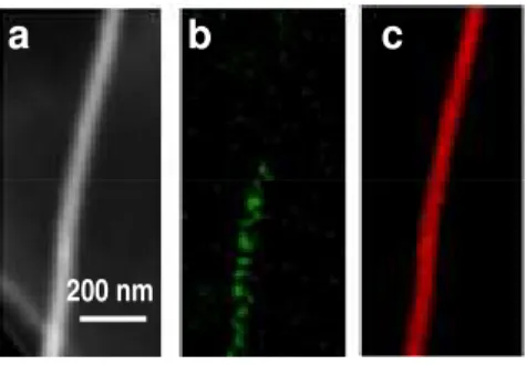
Figure 1. Z-contrast STEM images (a) and EDX compositional maps obtained using the Ge Kα (b) and Si Kα(c) X-ray lines of SiGe/Si nanowire heterostructures grown with Ga-Au metal droplets (50% Ga).
a b c
a b c
200 nm
a b c
a b c
RAMAN SPECTROSCOPY OF SiGe NWs
The Raman spectrum of NWs, and SiGe NWs in particular, contain a high degree of ambiguity, because, the one phonon band shape is sensitive to different factors, which are difficult to separate each other. In previous works [8], we have discussed the different contributions to the shape of the one phonon Raman spectrum of Si NWs. The measurement of the Raman spectrum of NWs is not a trivial experimental problem, especially when measuring individual NWs. The Raman signal is proportional to the sampling volume; therefore, the small volume occupied by the NWs inside the exciting laser spot strongly constrains the experimental measurement of the Raman spectrum of NWs. Regarding the SiGe alloys the composition is an additional source of complexity, because it can be a source of incertitude face to different factors that can change the Raman spectrum, e.g. temperature, stress, phonon confinement; therefore, one needs to control the experiment in order to assess the local composition changes [8, 9].
The measurement of the Raman spectrum of individual NWs demands a specific experimental protocol, because the diameter of the NW is well below the lateral resolution of the optical microscope. A Raman spectrum of an individual NW without a relevant contribution of laser induced heating can only be achieved when the thermal bonding between the NW and the support is very efficient, or when the configuration permits electromagnetic amplification to take place [10], which permits to lower the laser power down to values for which local induced heating is negligible.
NWs can be free standing, either in air or deposited on a substrate but with poor thermal contact, which the dielectric mismatch with the NW will be crucial for the intensity of the Raman signal. When the NWs are free standing in air the Raman signal of an individual NW is very weak, being very difficult to avoid laser induced heating if one wants to have a manageable signal. On the other hand, because of the nanometer dimension of the NWs diameter one needs to dispose of NW localization markers visible in the optical microscope in order to achieve the Raman measurements. The NW diameter is substantially smaller than the laser spot at focus, which has a Gaussian like power distribution; therefore, the effective excitation power of a NW depends on the position that it occupies inside the laser spot [11]. Due to the difficulty of placing the center of the focused laser beam onto the NW, the only way to achieve reliable measurements without the above mentioned uncertainty is performing Raman maps of the NWs. Once the position of the NW is localized using the markers, one launches a micro-Raman map scanning over the selected area enclosing the NW. The map must be carried out with submicrometric steps, e.g. 0.1 µm. Once the Raman map is achieved it is confronted to the SEM image of the NW establishing the spatial correlation between the Raman signature and the NW.
Regarding the composition assessment of the SiGe NWs, the one phonon Raman spectrum of Si1-xGex alloys consists of three major bands peaking around, 300, 400 and
500 cm-1. These bands correspond to the optical phonons associated with Ge-Ge, Si-Ge and Si-Si vibrations respectively. Their respective Raman parameters (frequency, intensity and linewidth) depend on the composition of the alloy. In the case of the frequencies, the relationships that account for their dependence on the composition are
ωSi-Si=520.7-66.9·x, ωGe-Ge=280.3+19.4·x and ωSi-Ge=400.1+24.5·x-4.5·x2-33.5·x3 [5]. The
Figure 2. Raman spectrum of a SiGe NW (a), Raman spectrum of the NW and Raman spectrum of a bulk Si sample, showing the strong resonance of the NW signal (b). (excitation 532 nm)
A typical Raman spectrum obtained in a SiGe NW with 532 nm excitation is shown in Fig.2-a. It presents the typical bands corresponding to Ge-Ge, Si-Si and Si-Ge bonds, plus an additional band related to the surface, that will not be discussed here. When the NW is deposited on an Al metallised glass surface the electric field inside the NW is more intense; being the Raman intensity per unit volume several orders of magnitude more intense than the Raman signal obtained in a bulk Si substrate, note that the composition of the NW is very low in Ge (∼10%), therefore, the Raman intensity does not greatly differ from that of pure Si, Fig. 2-b; such behaviour does not happen for a NW standing in air, for which the signal was very weak under the same excitation conditions. The Raman spectrum of the SiGe NW presents the typical bands corresponding to Si-Si, Si-Ge and Ge-Ge bonds.
Figure 3. SEM image of a SiGe NW; the red dot represents the laser beam (a). Composition along the NW as deduced from the Si-Si Raman and the Ge-Ge Raman peaks respectively (b).
The Raman parameters obtained from the spectra along the NW, Fig. 3, evidence that the alloy composition along the NW deduced from either the Si-Si mode frequency or the Ge-Ge mode frequency does not match; while the composition deduced from the Si-Si mode fits well the composition determined by EDX in the TEM and the nominal
a)
bbbbb
b)
Ge-Ge Si-Ge Si-Si
Defect band
Ge-Ge Si-Ge Si-Si
Defect band
a
composition of the NW (∼10-12% Ge), the composition deduced from the Ge-Ge mode gives a much higher Ge content; in fact, this behaviour is the consequence of the existence of a rich Ge shell surrounding the NW, which the origin might be the oxidation of the NW, with the result of a core-shell structure formed by the SiGe core and a thin shell of different composition very rich in Ge. This core-shell structure is responsible for the inaccuracy in the estimation of the NW composition from the Raman intensities [9], cross sectional EDX reveals a thin Ge rich shell, not shown here. In fact, the Raman spectrum measured is the convolution of the SiGe core and the Ge-rich shell, Fig. 4. Note that the diameter of the NWs is higher than 25 nm, which permits to neglect the influence of the phonon confinement in the Raman frequencies.
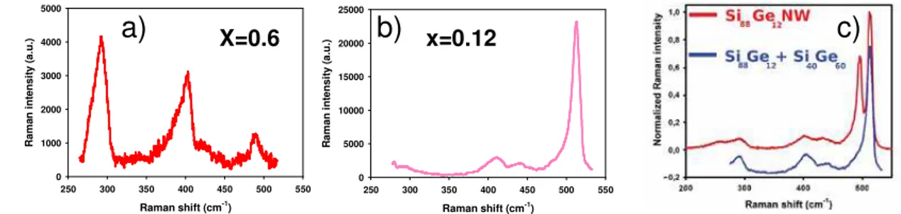
Figure 4. Raman spectra of SiGe layers with x = 0.6 (a) and x = 0.12 (b), the convolution of the two spectra gives an spectrum similar to the one obtained in a NW with x = 0.12 (c).
Figure 5. Electric field (E2) inside NWs of different diameters.
Both contributions are not simply added by weighting their corresponding volumes, but depend on the distribution of the electric field inside the NW, which is determined by the interaction between the electromagnetic field of the laser radiation and the NW. The electric field distributions obtained by solving the Maxwell equations using finite element methods inside NWs of different diameters are shown in Fig. 5. One observes that the electric field is not homogeneously distributed inside the NW. Therefore, in inhomogeneous NWs, as core-shell structures, the Raman spectrum can present important distortions depending on the diameter that fuzzy its interpretation.
In the case of axial heterostructures, the junction can be localized by mapping the Raman signal along the NW. Fig. 6 shows the Raman intensity of the Si section along the NW axis; one observes the progressive decrease of the Raman intensity of pure Si when the laser spot starts to share the two NW sections. The junction can be situated by the derivative of the intensity plot. However, the accurate determination of the heterojunction requires high resolution Raman maps.
Raman shift (cm-1)
250 300 350 400 450 500 550
R a m a n i n te n s it y ( a .u .) 0 5000 10000 15000 20000 25000
Raman shift (cm-1)
250 300 350 400 450 500 550
R a m a n i n te n s it y ( a .u .) 0 1000 2000 3000 4000 5000
X=0.6 x=0.12
a) b)
c)
Raman shift (cm-1)
250 300 350 400 450 500 550
R a m a n i n te n s it y ( a .u .) 0 5000 10000 15000 20000 25000
Raman shift (cm-1)
250 300 350 400 450 500 550
R a m a n i n te n s it y ( a .u .) 0 1000 2000 3000 4000 5000
X=0.6 x=0.12
Raman shift (cm-1)
250 300 350 400 450 500 550
R a m a n i n te n s it y ( a .u .) 0 5000 10000 15000 20000 25000
Raman shift (cm-1)
250 300 350 400 450 500 550
R a m a n i n te n s it y ( a .u .) 0 1000 2000 3000 4000 5000
X=0.6 x=0.12
Figure 6. Intensity of the Raman signal of the Si section of the axial heterojunction as a function of the position of the center of the beam spot. The derivative places the position of the heterojunction. Note that the beam diameter is ≈1µm.
SUMMARY
The Raman spectrum of SiGe NWs has been stdudied. The Raman spectrum of individual NWs without laser heating effects can be measured under resonance conditions. Core shell heterostructures formed by oxidation are studied considering the interaction between the laser beam and the NW. Finally, axial heterostructures can be localized by high resolution Raman maps.
ACKNOWLEDGMENTS
This work was funded by the Spanish Government (Grant: MAT2010-20441-C02-01-02) and JCYL (VA293U13). The TEM work has been carried out at the LABMET of the CAM, Madrid.
REFERENCES
[1] J. Li, H.Y. Yu, S. M. Wong, X. Li,G. Zhang, P. G.-Q. Lo, D.-L. Kwong; Appl. Phys. Lett. 95, 243113 (2009).
[2] P. Pichanusakorn, P. Bandaru; Mater. Sc. Eng. R 67, 19 (2010).
[3] T. J. Kempa, J. F. Cahoon, S. K. Kim, R. W. Day, D. C. Bell, H. G. Park, C. M. Lieber; PNAS 109, 1407 (2012).
[4] T. E. Clark, P. Nimmatoori, K. K. Lew, L. Pan, J. M. Redwing, E. C. Dickey, Nano Lett. 8, 1246 (2008).
[5]F. Pezzolli, L. Martinelli, E. Grilli, M. Guzzi, S. Sanguinetti, M. Bollani, H. D. Chrastina, G. Isella, H. von Kanel, E. Winsterberger, J. Stangl, G. Bauer; Mater. Sci. Eng. B 124, 127 (2005).
[6] Q. Lu, K. W. Adu, H. R. Gutiérrez, G. Chen, K-K. Lew, P. Nimmatoori, X. Zhang, E. C. Dickey, J. M. Redwing, P. C. Eklund ; J. Phys. Chem. C112, 3209 (2008)
[7]A. Rodríguez, T. Rodríguez, C. Ballesteros, J. Jiménez; Mat. Res. Soc. Symp. Proc.
1510, DD06-05 (2013).
[8] J. Anaya, A.Torres, A. C. Prieto, V. Hortelano, J. Jiménez, A. Rodríguez, T. Rodríguez; Appl. Phys. A, DOI:10.1007/S00339-013-7966y (2013).
[9] C. Nishimura, G. Imamura, M. Fujii, T. Kawashima, T. Saitoh, S. Hayashi; Appl. Phys.Lett. 93, 203101 (2008).
[10] L. Cao, J. S. White, J. S. Park, J. A. Schuller, B. Clemens, M. L.Brongersma; Nature Mater. 8, 643 (2009).
[11] J. Anaya, A. Torres, A. Martín-Martín, J. Souto, J. Jiménez, A. Rodríguez, T. Rodríguez; Appl. Phys. A 113, 167 (2013).
0.0 0.2 0.4 0.6 0.8 1.0
D e ri v a ti v e i n te n s it y ( a .u .) 0.00 0.01 0.02 0.03 0.04 0.05 0.06
distance along axis (µµµµm)
R a m a n i n te n s it y ( a .u .) 0.0 0.2 0.4 0.6 0.8 1.0 Si SiGe
0.0 0.2 0.4 0.6 0.8 1.0
D e ri v a ti v e i n te n s it y ( a .u .) 0.00 0.01 0.02 0.03 0.04 0.05 0.06
distance along axis (µµµµm)
R a m a n i n te n s it y ( a .u .) 0.0 0.2 0.4 0.6 0.8 1.0


![Assignment of the Raman Spectrum of Benzylic Amide [2]Catenane: Raman Microscopy Experiments and First-Principles Calculations](data:image/gif;base64,R0lGODlhAQABAIAAAP///wAAACH5BAEAAAAALAAAAAABAAEAAAICRAEAOw==)