Analysis of the electrical behavior of silicon rich silicon oxides
6
0
0
Texto completo
(2) 7a Reunión Española de Optoelectrónica, OPTOEL’11. (a) Vertical layout of the device. (b) Measurement setup. Figure 1: Vertical layout of the device and measurement setup active layer is grown/deposited on a 0.1–1.4 Ω·cm silicon substrate. Three sets of samples will be studied here, each with its active layer fabricated by one of the previously mentioned CMOS compatible techniques, namely LPCVD, PECVD and ion implantation. The LPCVD and PECVD SRO layers were obtained adjusting the ratio between the precursor gases ([SiH4 ]/[N2 O]). Samples with different ratios have been fabricated, thus leading to different silicon excesses in the active layers. More details on the preparation of the SRO samples have been published for LPCVD[13] and PECVD[7]. For the implanted samples, a 40 nm thick thermal silicon oxide is grown on the silicon substrate, followed by the deposit of a 30 nm thick silicon nitride layer used to control the silicon implantation process, which was removed after the annealing process. Two silicon ion implantations were carried out[14] in each sample with varying doses (between 1.2 · 1016 and 8.3 · 1016 cm−2 ): the first one at 25 KeV and the second one at 50 KeV. The implanted dose during the 50 keV process is four times the implanted dose during the 25 keV implantation. This ratio between the 25 and 50 keV implantations leads to a rather homogeneous distribution of the implanted silicon ions across the silicon oxide layer according to SRIM[15] Technique LPCVD. PECVD. Ion Implantation. Si. exc [%] 6 7 19 6 8 12 16 12 13 14 15 17. simulations. The experimentally obtained silicon excesses and thicknesses of all the samples can be found in table 1 Once an SRO layer is obtained, a thermal annealing is carried out to induce the formation of silicon nanoparticles in the dielectric layer[7, 13, 14]. The selection of annealing temperatures and durations have been based on previous results[7, 13, 14] and are referenced in table 1. In the case of the ion implanted samples, the silicon nitride layer used during the implantation process is removed after the annealing. The device fabrication continues with the deposition and doping process of a 350 nm n–type polysilicon layer followed by photolitography and etching to define the transversal layout of the gate (squares of sides 500 µm). Next, an aluminum layer of 1000 nm is deposited followed by a second photolitography step and etching process to define the contact pads. Finally, the back contact is formed by sputtering of an aluminum layer followed by an annealing process. The electrical measurements were performed in a Karl Süss probe station, with Süss Microtech PH120 probeheads and 7 µm tungsten probes. Current-voltage characteristics were obtained with a Keithley 2430 source-meter and capacitance-voltage. Thickness [nm] 53 ± 3 35 ± 5 20 ± 3 53 ± 5 55 ± 6 60 ± 9 59 ± 7 40 ± 5 43 ± 4 44 ± 9 44 ± 4 22 ± 1. Ann. temp. [o C]. Ann. duration [min]. 1100. 180. 1250. 60. 1100. 240. Table 1: Sample characteristics according to the fabrication technique. -2-. J. JUVERT et al..
(3) 7a Reunión Española de Optoelectrónica, OPTOEL’11. (a) C–V characteristics. (b) I–V characteristics. Figure 2: Electrical characteristics obtained in LPCVD samples with 6% silicon excess. (a) C–V characteristics. (b) I–V characteristics. Figure 3: Electrical behavior of PECVD samples with 6% and 16% silicon excess characteristics were measured with an HP 4192A LF impedance analyzer. The measurement protocol has been the same in all samples: firstly, capacitance-voltage characteristic is measured on as-obtained devices (those that have never been electrically stressed previously in any way). Secondly, current-voltage characteristics are measured. Finally the C–V is again measured after the I-V stress. Capacitance–voltage curves have been taken from inversion to accumulation and back to inversion with a voltage ramp of 0.1 V/s and the AC component of the ramp at 100 KHz.. 3. representative samples have been plotted. In order to eliminate the dependence of the capacitance on the area and thickness of the device, the values have been multiplied by the thickness of the device and divided by its area and the permittivity of vacuum. Therefore, the values of the y–axis of the C–V curves are adimensional and the saturation value in accumulation (negative voltages) tends to the relative permittivity of the medium. The samples fabricated by LPCVD show two different behaviors: on as-obtained devices the C–V curve is quite anomalous (red line, figure 2(a)). This corresponds to the high leakage current shown in figure 2(b) (red line). In this state, electroluminescence can be seen as bright spots on the surface of the device. At some point during the electrical stress, the current drops to a low leakage situation[16]. At the same time the luminescent dots disappear[17]. Once in low leakage, the device remains in that state (see green line in figure 2(b), a second I–V measurement). Moreover, if. Results. Figures 2 to 5 show typical C–V and I–V behaviors of samples with different silicon excess and fabricated using different techniques. For clarity, only the most. -3-. J. JUVERT et al..
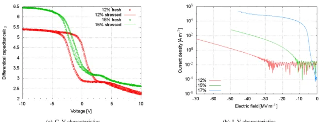
(4) 7a Reunión Española de Optoelectrónica, OPTOEL’11. (a) C–V characteristics. (b) I–V characteristics. Figure 4: Electrical characteristics of implanted samples with 12% and 15% silicon excess. Figure 5: Anomalous C–V curve of the implanted sample with 17% silicon excess we measure capacitance again, the C–V curve now resembles that of a regular MOS capacitance (see green line in figure 2(a)). While in low leakage, homogeneous luminescence in the whole area of the device can be detected from around 1.0 A · m−2 .. is related to a low leakage current density (see figure 3(b)) and to homogeneous electroluminescence at around 1.0 A·m−2 . No luminescent dots are observed in PECVD samples. The current density increases with silicon excess. However, samples with higher silicon excess are also more prone to breakdown. As a result, luminescence appears at lower voltages but the maximum achievable current before breakdown is also lower.. Figures 3(a) and 3(b) show the typical behavior of PECVD samples with different silicon excess. The C–V characteristics are quite similar to the expected from a MOS capacitance. Deep depletion can be observed in most samples and a displacement of the flat band voltage before and after the electrical stress can be seen for the lower silicon excesses. According to the hysteresis cycle, the amount of trapped charge and the oxide capacitance both increase along with silicon excess. The former is related to the increase of the density and size of the silicon nanoparticles[18]. From the latter we can infer an increase of the effective permittivity of the medium with the silicon excess[2], which is clear in the adimensional scale chosen for the y–axis of the C–V plots.. Ion Implanted samples show a slightly different C– V behavior (figure 4(a)). According to the width of the hysteresis cycle, the amount of trapped charge decreases as silicon excess is increased. There is also very little change in the C–V curves before and after the electrical stress. As with the PECVD samples, the relative permittivity of the medium increases with silicon excess, although there is little difference between the samples with 14% and 15% silicon excess. The samples with silicon excesses from 12% to 15% present homogeneous electroluminescence in the whole area from 1.0 A · m−2 .. As with the LPCVD samples, a regular C–V curve. -4-. J. JUVERT et al..
(5) 7a Reunión Española de Optoelectrónica, OPTOEL’11. The sample with 17% silicon excess presents an unstable C–V curve (figure 5) as well as high leakage current (figure 4(b), blue line). Similarly to what happened in the high leakage state in the LPCVD samples, no homogeneous electroluminescence is observed in this sample. Instead, only luminescent dots can be seen. In the IV curves of the implanted samples it is also observed that the current density increases with silicon excess. The considerations about breakdown that we have discussed for the PECVD samples also apply here, although the differences are much less apparent, most likely due to the relatively small difference in silicon excess between samples.. 4. Acknowledgements A. González acknowledge the grant No. 213571 received from the CONACyT of México.. References [1] L. T. CANHAM, “Silicon quantum wire array fabrication by electrochemical and chemical dissolution of wafers“, Applied Physics Letters, 57, 1046, 1990 [2] J. BARRETO et al, ”Pulsed electroluminescence in silicon nanocrystals-based devices fabricated by PECVD“, Physica E: Lowdimensional Systems and Nanostructures, 38, 193-196, 2007 [3] D. J. DIMARIA et al, ”Electroluminescence studies in silicon dioxide films containing tiny silicon islands“, Journal of Applied Physics, 56, 401-416, 1984. Conclusions. We have shown the C-V and I-V behavior of MOS structures featuring silicon nanoparticles embedded in its dielectric matrix. We have seen that there are two possible conduction regimes, one with low leakage and one with high leakage. The high leakage regime seems to be related to the formation of a finite number of conductive paths across the dielectric matrix. In this situation, almost all the current flows through those conductive paths. Therefore, the conduction through the active layer is not uniform and light is only observed in points corresponding to the places where the conduction takes place. On the other hand, in the low leakage regime there are no such conductive paths and the current flows uniformly through the whole area of the layer. Accordingly, light emission also occurs uniformly in the whole area of the device. The studied PECVD samples do not show a high leakage regime, whereas for implanted samples only the highest silicon excess shows such regime. The LPCVD sample presents both kinds of leakage: asobtained devices show high leakage, which turns into low leakage after the application of an electrical stress. This behavior has been attributed to the annihilation of the preferential conductive paths[16]. It has also been shown that the low leakage regime is related to a regular MOS-like C-V behavior, whereas samples in high leakage regime show anomalous C-V, most likely related to the instability of the conductive paths. A remarkable fact is that all the devices have a threshold current density of 1.0 A · m−2 before the emission starts, independently of the fabrication technique. This threshold is achieved at different electric fields depending on the silicon excess and the fabrication technique.. [4] G. FRANZÒ et al, ”Electroluminescence of silicon nanocrystals in MOS structures“, Applied Physics A, 74, 1-5, 2002 [5] A. IRERA et al, ”Excitation and de-excitation properties of silicon quantum dots under electrical pumping“, Applied Physics Letters, 81, 1866, 2002 [6] A. MORALES et al, ”Blue and red electroluminescence of silicon-rich oxide light emitting capacitors“, in Proceedings of SPIE Photonics Europe, 52, 2010 [7] M. PERÁLVAREZ et al, ”Field effect luminescence from Si nanocrystals obtained by plasmaenhanced chemical vapor deposition“, Applied Physics Letters, 89, 051112, 2006 [8] Z. H. CEN et al, ”Strong violet and greenyellow electroluminescence from silicon nitride thin films multiply implanted with Si ions“, Applied Physics Letters, 94, 041102, 2009 [9] L. DAL NEGRO et al, ”Light emission efficiency and dynamics in silicon-rich silicon nitride films“, Applied Physics Letters, 88, 233109, 2006 [10] R. HUANG et al, ”Enhanced electroluminescence efficiency of oxidized amorphous silicon nitride light-emitting devices by modulating Si/N ratio“, Applied Physics Letters, 91, 111104, 2007 [11] D. LI et al, ”Enhanced electroluminescence of silicon-rich silicon nitride light-emitting devices by NH3 plasma and annealing treatment“, Physica E: Low-dimensional Systems and Nanostructures, 41, 920-922, 2009. -5-. J. JUVERT et al..
(6) 7a Reunión Española de Optoelectrónica, OPTOEL’11. [12] A. MORALES et al, ”Spectroscopical analysis of luminescent silicon rich oxide films“, Rev. Mex. Fis. S, 53, 279-282, 2007. [16] A. MORALES et al, ”The mechanism of electrical annihilation of conductive paths and charge trapping in silicon-rich oxides“, Nanotechnology, 20, 45201, 2009. [13] A. MORALES et al, ”Coulomb blockade effects in silicon nanoparticles embedded in thin silicon-rich oxide films“, Nanotechnology, 19, 165401, 2008. [17] A. A. G. FERNÁNDEZ et al, ”Intense whole area electroluminescence from low pressure chemical vapor deposition-silicon-rich oxide based light emitting capacitors“, Journal of Applied Physics, 108, 043105, 2010. [14] M. PERÁLVAREZ et al. ”Si-nanocrystal-based LEDs fabricated by ion implantation and plasma-enhanced chemical vapor deposition“, Nanotechnology, 20, 405201, 2009. [18] A. MORALES et al, ”Optical characterization of silicon rich oxide films“, Sensors and Actuators A: Physical, 142, 12-18, 2008. [15] http://www.srim.org/. -6-. J. JUVERT et al..
(7)
Figure


Documento similar
H I is the incident wave height, T z is the mean wave period, Ir is the Iribarren number or surf similarity parameter, h is the water depth at the toe of the structure, Ru is the
Keywords: Metal mining conflicts, political ecology, politics of scale, environmental justice movement, social multi-criteria evaluation, consultations, Latin
In the previous sections we have shown how astronomical alignments and solar hierophanies – with a common interest in the solstices − were substantiated in the
teriza por dos factores, que vienen a determinar la especial responsabilidad que incumbe al Tribunal de Justicia en esta materia: de un lado, la inexistencia, en el
Even though the 1920s offered new employment opportunities in industries previously closed to women, often the women who took these jobs found themselves exploited.. No matter
Our results here also indicate that the orders of integration are higher than 1 but smaller than 2 and thus, the standard approach of taking first differences does not lead to
Although some public journalism schools aim for greater social diversity in their student selection, as in the case of the Institute of Journalism of Bordeaux, it should be
In the “big picture” perspective of the recent years that we have described in Brazil, Spain, Portugal and Puerto Rico there are some similarities and important differences,
