Combined grazing incidence RBS and TEM analysis
of luminescent nano-SiGe/Si0
2multilayers
A. Kling , A. Rodriguez , J. Sangrador , M.I. Ortiz , T. Rodriguez ,
C. Ballesteros , J.C. Soares
Centre* de Fisica Nuclear da Universidade de Lisboa, Av. Prof. Gama Pinto 2, 1649-003 Lisboa, Portugal Instituto Tecnologico e Nuclear, Estrada Nacional n°10, 2686-953 Sacavem, Portugal
Departamento de Tecnologia Electronica, ETSI de Telecomunicacion, Universidad Politecnica de Madrid, 28040 Madrid, Spain Departamento de Fisica, Escuela Politecnica Superior, Universidad Carlos III, 28911 Leganes, Madrid, Spain
Abstract
Multilayer structures with five periods of amorphous SiGe nanoparticles/Si02 layers with different thickness were deposited by Low
Pressure Chemical Vapor Deposition and annealed to crystallize the SiGe nanoparticles. The use of grazing incidence RBS was necessary to obtain sufficient depth resolution to separate the signals arising from the individual layers only a few nm thick. The average size and areal density of the embedded SiGe nanoparticles as well as the oxide interlayer thickness were determined from the RBS spectra. Details of eventual composition changes and diffusion processes caused by the annealing processes were also studied. Transmission Electron Microscopy was used to obtain complementary information on the structural parameters of the samples in order to check the informa-tion yielded by RBS. The study revealed that annealing at 900 °C for 60 s, enough to crystallize the SiGe nanoparticles, leaves the struc-ture unaltered if the interlayer thickness is around 15 nm or higher.
Keywords: Nanostructure multilayers; SiGe nanoparticles; LPCVD; Grazing incidence RBS; TEM
1. Introduction
Si, SiGe and Ge nanoparticles embedded in an oxide matrix are highly interesting for applications in lumines-cent devices compatible with CMOS technology A promising method for the production of this kind of struc-tures is the deposition of amorphous SiGe nanoparticles embedded in Si02 using a conventional hot tube Low
Pressure Chemical Vapor Deposition reactor operating
at low temperatures followed by a thermal treatment to crystallize them. These structures exhibit luminescent emis-sion peaking in the blue-violet at 400 nm The influence of the thermal treatment processes on the structure of the samples has to be investigated in order to optimize the annealing conditions to get the maximum luminescence intensity. Since the luminescence in single discontinuous layers is limited by the number of nanoparticles that can be placed in a plane, the use of multilayer structures is of high interest to increase the light output In the pres-ent study, the structural properties of as-deposited and annealed multilayers with different nanoparticle sizes and Si02 interlayer thicknesses have been investigated and
2. Experimental details
Multilayer structures with five layers of amorphous SiGe nanoparticles and six identical Si02 layers were deposited
on Si wafers in a continuous process using a commercial LPCVD reactor. The total pressure and temperature were kept constant at 50 mTorr and 390 °C, respectively. The discontinuous SiGe layers (i.e. the SiGe nanoparticle con-taining layers) were deposited using Si2H6 and GeH4.
Keep-ing a flow ratio of GeH4/Si2H6 = 0.82 allowed a Ge fraction
of x K, 0.4 to be achieved. The Si02 layers were produced
using Si2H6 and 02 with a flow ratio of Si2H6/02 = 0.2.
The thickness of both types of layers was controlled by the deposition time. More details on the system and on the deposition process can be found elsewhere Sam-ples with multilayer structures combining two different SiGe nanoparticle sizes with thin (5 nm), intermediate (15 nm) and thick (35 nm) Si02 interlayers (nominal
thick-ness) were deposited (see Table 1 for the sample identifica-tion and their characteristics).
The samples were subjected to heat treatments at temper-atures between 700 °C and 900 °C in N2 atmosphere and for
times up to 60 s using a Rapid Thermal Annealing (RTA) unit in order to induce crystallization. Sample D was also subjected to annealing in a conventional open tube furnace under N2 atmosphere at temperatures of 900 °C and
1000 °C for 1 h to investigate the eventual degradation for higher temperatures and longer annealing times.
Grazing incidence RBS measurements with a 2 MeV
4H e+ ion beam impinging on the target at angles between
72° and 82 ° were used to obtain sufficiently high depth res-olution to separate the signals arising from the different layers and to detect and investigate possible compositional changes. The Si surface barrier detector was located at 160° with respect to the incident beam in Cornell geometry. Cross-sectional specimens suitable for high-resolution transmission electron microscopy (HRTEM) were pre-pared by standard procedures. TEM images were obtained using a Philips Tecnai 20F FEG analytical microscope operating at 200 keV, equipped with EDX.
Photoluminescence measurements were performed at room temperature using the 315 nm line of a He-Cd laser for excitation.
3. Results and discussion
In a first step the as-deposited multilayer structures, which serve as a reference, were characterized by TEM
and grazing incidence RBS to determine the composition, diameter and areal density of the embedded SiGe nanopar-ticles as well as the thickness of the Si02 interlayers. A
model recently developed by the authors using RUMP for the analysis of RBS spectra of samples containing embedded nanoparticles was used for these purposes. The results of the TEM and RBS studies are summarized in Table 1 showing a good agreement. The size and spatial distribution of the nanoparticles located in the different layers exhibit a good uniformity and the thickness of the different oxide interlayers of each sample is repetitive. The EDX spectra obtained in very thin areas of the as-deposited samples as well as the RBS spectra fittings are consistent with the nominal value of the Ge fraction, x « 0.4. Unless otherwise specified, the data obtained by RBS are used from now on throughout the text.
The TEM micrographs of three of the samples (B, C and D) after RTA treatment at 900 °C for 60 s, shown in Fig. 1, revealed that the morphology of the samples after anneal-ing remains unaltered compared to the as-deposited ones (not shown), preserving the nanoparticle size and the aver-age nanoparticle density. In sample B (and also in A, not included), due to the two-dimensional projection of the three-dimensional sample, the layers appear to be continu-ous. Higher magnification studies carried out in very thin areas indicate that the layers are discontinuous, although the areal density of nanoparticles could not be estimated because the nanoparticles appear superimposed to each others in the images. The analysis of the TEM images of samples C and D allows the minimum areal density of nanoparticles to be estimated and it is always above 5 x 1011 cm~2 in each layer.
Although the TEM studies indicate that the multilayer structures in these three samples are intact after the RTA treatments, grazing incidence RBS measurements were per-formed to check for eventual compositional changes that are not detected by TEM.
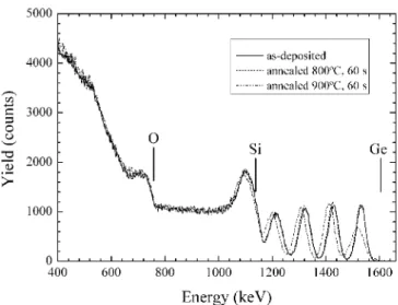
Fig. 2 shows the RBS spectra of sample A, which has the thinnest (3-3.3 nm) Si02 interlayers and larger
nanoparti-cles (ca. 7 nm in diameter), in the as-deposited state and after RTA annealing at 800 °C for 30 s and 900 °C for 60 s. The separation of the Ge signals stemming from the nanoparticle layers was only possible using a tilt angle of
9 = 82°. While for annealing at 700 °C (not shown) and
800 °C the RBS spectra virtually overlap with the one of the as-deposited sample, after annealing at 900 °C a strong degradation of the multilayer structure is observed. A detailed analysis of the RBS spectra shows that about half
Table 1
SiGe nanoparticle diameters, areal densities of nanoparticles and Si02 interlayer thickness determined by TEM and RBS
Sample Values determined by TEM Values determined by RBS
Fig. 1. TEM images of samples B, C and D (see text and Table 1) after RTA at 900 °C, 60 s.
5000
- as-deposited - annealed 800°C, 30 s • annealed 900°C, 60 s
400 600 800 1000 1200
Energy (keV)
1400 1600
Fig. 2. Grazing incidence RBS spectra (9 = 82°) of sample A in the as-deposited state and after RTA at 800 °C and 900 °C.
5000
as-deposited annealed 800°C, 60 s annealed 900°C, 60 s
Ge
400 600 800 1000 1200 1400 1600
Energy (keV)
Fig. 3. Grazing incidence RBS spectra (9 = 78°) of sample B in the as-deposited state and after RTA at 800 °C and 900 °C.
of the Ge originally contained in the three top SiGe nano-particle layers has been lost. One fraction seems to have left the sample by outdiffusion while another fraction has dif-fused into the adjacent Si02 interlayers and into the fourth
layer from the top. The Ge content of this layer increased significantly with regard to the as-deposited sample as can be seen from the enhanced RBS yield. The fifth layer located next to the Si substrate has virtually not been affected by the annealing. The results of the RUMP fit using the nanoparticle model indicate that the size of the remaining SiGe nanoparticles in the three top layers has been reduced to an average diameter of about 4 nm.
In the case of sample B, which has nanoparticles with the same average diameter as sample A (ca. 7 nm) but much thicker (33-35 nm) Si02 interlayers, the RBS spectra
(Fig. 3) taken at a tilt angle of 9 = 78°, in this case sufficient to resolve the SiGe nanoparticle layers, also show that the RTA at 800 °C leaves the structure unchanged. Compared to sample A the degradation after RTA at 900 °C for 60 s is strongly reduced and affects only the SiGe nanoparticle layer located closest to the surface.
The RBS spectra of sample C (Fig. 4), which contains smaller SiGe nanoparticles (ca. 4 nm diameter), taken at
9 = 82° (in order to resolve the SiGe layers despite the
12-15 nm thick interlayers) show that the RTA at 800 °C and 900 °C has virtually no effect on the layer structure with Si02 interlayers thicker than those of sample A.
Indi-cations of a slight Ge diffusion towards the interface have been found after RTA at 800 °C for 30 s using a slightly lower tilt angle of 80.8° (not shown). Due to the reduced separation of such a thin layer from the last SiGe layer and the Si substrate at 9 = 82° and the enhanced straggling at this depth a quantitative determination of the Ge amount at the interface was not feasible.
- as-deposited - annealed 800°C, 30 s • annealed 900°C, 60 s
400 600 800 1000 1200
Energy (keV)
1400 1600
Fig. 4. Grazing incidence RBS spectra (9 = 82°) of sample C in the as-deposited state and after RTA at 800 °C and 900 °C.
400 600 800 1000 1200
Energy (keV)
1400 1600
Fig. 6. Grazing incidence RBS spectra (9 = 72°) of sample D in the as-deposited state and after furnace annealing at 900 °C and 1000 °C.
at the interface with the Si substrate is 2.2 x 10¹⁵ c m- 2 and
4.4 x 10¹⁵ c m- 2 in the samples annealed at 800 °C and
900 °C, respectively. Annealing of this sample for 1 h leads at all the investigated temperatures (900 °C and 1000 °C) to a significant alteration of the multilayer structures as can be seen in the RBS spectra of Fig. 6. Annealing at 900 °C leads to the formation of a discontinuous Ge layer (ca. 9 x 1015 cm- 2) at the interface with the Si substrate, while
annealing at 1000 °C also causes the Ge to diffuse into the substrate. A further interesting effect is that after annealing at 900 °C for 30 or 60 s the structure remains almost intact except for the slight Ge diffusion processes, but if the annealing time is increased up to 1 h or the temperature is raised up to 1000 °C the layers located close to the Si substrate are strongly affected by the diffusion while the top layer of nanoparticles is not strongly affected, so the degradation of this specific sample takes place mostly by diffusion from all layers towards the substrate and only
slightly towards the outer surface of the sample. In addi-tion to the structural features of the sample, other factors like the enhanced densification of the oxide layers could play a role in the observed behavior.
A recently published study on the optimization of the luminescent properties of these samples shows that the cathodoluminescence intensities of samples B, C and D increase with RTA treatment temperature and time up to 900 °C and 60 s, respectively. The relative luminescence intensities of these samples are 25 (B), 10 (C) and 300 (D) indicating that the luminescence is optimized by the simultaneous presence of Ge diffusion limiting thick inter-layers and small nanocrystals. These results are corrobo-rated by photoluminescence measurements performed at room temperature. Fig. 7 shows the results for sample D which shows the largest luminescence enhancement. Sample A shows a reduced luminescence at these treatment
8000
as-deposited annealed 800°C, 60 s annealed 900°C, 60 s
400 600 800 1000 1200
Energy (keV)
1400 1600
Fig. 5. Grazing incidence RBS spectra (9 = 72°) of sample D in the as-deposited state and after RTA at 800 °C and 900 °C.
1000
900°C, 60s
400 450 500 550
Emission wavelength (nm)
600
conditions which is a result of the degradation of the mul-tilayer structure.
4. Conclusions
RBS characterization of multilayers of SiGe nanoparti-cles/Si02 using grazing angles resolved the signals of the
different layers of nanometric thickness in the spectra, thus making possible the analysis of the structure of the samples and the study the effect of the annealing processes on this structure.
The detailed characterization of the important structural properties of SiGe nanoparticle/Si02 multilayer structures
(composition, diameter and areal density of the nanoparti-cles as well as the thickness of the oxide interlayers) has been carried out using a model developed by the authors to produce an input for the RUMP code. The obtained results are in agreement with those derived from the TEM analysis of the samples, which were used as a refer-ence for comparison.
The RBS study revealed that annealing of the multilay-ers at 900 °C for 60 s, which are conditions that produce the crystallization of the nanoparticles, keeps the main structural features of the multilayers unaltered if the Si02
interlayers are thick enough (above 12-15 nm).
Acknowledgments
This work was funded by the Spanish Government through CICYT Project MAT2004-04580-C02 and a com-mon Grant by CRUP (Portugal) and MCT (Spain) in the framework of the Accoes Integradas/Acciones Integradas Program. TEM work has been carried out at the LABMET of the CAM (Madrid). The authors would like to thank M. Avella and J. Jimenez (Universidad de Valladolid, Spain) for the PL measurements.
References
M. Zacharias, L.X. Yi, J. Heitmann, R. Scholz, M. Reiche, U. Gosele, Solid State Phenom. 94 (2003) 131.
S.N.M. Mestanza, E. Rodriguez, N.C. Frateschi, Nanotechnology 17 (2006) 4548.
A. Rodriguez, M.I. Ortiz, J. Sangrador, T. Rodriguez, M. Avella, A.C. Prieto, J. Jimenez, A. Kling, C. Ballesteros, Phys. Status Solidi (A) 204 (2007) 1639.
M.I. Ortiz, J. Sangrador, A. Rodriguez, T. Rodriguez, A. Kling, N. Franco, N.P. Barradas, C. Ballesteros, Phys. Status Solidi (A) 203 (2006) 1284.