Characterization of a Mo/Au
Thermometer for ATHENA
María Parra-Borderías, Iván Fernández-Martínez, Lourdes Fábrega, Agustín Camón, Oscar Gil, José L. Costa-Kramer, Raquel González-Arrabal, Javier Sesé, Juan Bueno, and Fernando Briones
Abstract—The first dark characterization of a thermometer fabricated with our Mo/Au bilayers to be used as a transition edge sensor is presented. High-quality, stress-free Mo layers, whose thickness is used to tune the critical temperature ( 2 c ) down to 100 mK, are deposited by sputtering at room temperature (RT) on SÍ3N4 bulk and membranes, and protected from degradation with a 15-nm sputtered Au layer. An extra layer of high-quality Au is deposited by ex situ e-beam to ensure low residual resistance. The thermometer is patterned on a membrane using standard photolithographic techniques and wet etching processes, and is contacted through Mo paths, displaying a sharp superconducting transition ( a « 600). Results show a good coupling between Mo and Au layers and excellent Tc reproducibility, allowing to accurately correlate <1MO a nd Tc- Since d^u is bigger than
| M for all analyzed samples, bilayer residual resistance can be modified without affecting Tc- Finally, first current to voltage measurements at different temperatures are measured and ana-lyzed, obtaining the corresponding characterization parameters.
Index Terms—Proximity effect, radiation detectors, transition edge sensors.
I. INTRODUCTION
T
RANSITION Edge Sensors (TES) used as microcalori-meters or bolomicrocalori-meters are at the base of cryogenic radia-tion detectors in a wide range of frequencies, from millimeter waves [l]-[3] to gamma-rays [4]-[6]. These superconductingsensors, operated in the transition temperature region (usually ~100 mK), provide a sensitivity that can be two orders of mag-nitude higher than that for detectors based on semiconductor thermistors [7].
In the case of proximity effect bilayers, like the ones studied in this work, a low enough working temperature is obtained because of the reduction of Tc that a superconducting layer (S) thinner than its superconducting coherence length experiments when a normal metal layer (M) is deposited on top of it. The resulting bilayer, as a whole, behaves as a superconductor, with Tc determined by the thickness ratio between the S layer
and the M layer and the quality of the interface between both.
Mo/Au bilayers are especially interesting because of the lack of intermetallic compound formation at the interface below 800 °C, the Au high resistance to corrosion and the easy lithography. Moreover, we have shown that functional properties of Mo/Au bilayers are stable in the temperature range specified in the test of flight (T < 150 °C), which makes them competitive candidates for future space missions [8].
In previous works we demonstrated the capability to fabricate high quality, reproducible Mo/Au bilayers [9], [10]. Here we report on the fabrication and dark characterization of Mo/Au based thermometers to be used as TES detectors.
II. EXPERIMENTAL DETAILS
The temperature dependence of the electrical resistance and the superconducting critical temperature for Mo/Au layers were measured using the four-point resistance technique. Measure-ments were carried out in a commercial Physical Property Measurement System (PPMS) from Quantum Design, at the Physical Measurement Service of the University of Zaragoza. This system can perform resistivity measurements down to 350 mK. For temperatures in the range from 350 mK to 50 mK a commercial dilution refrigerator (Kelvinox MX40) from Oxford Instruments and an AVS-47 resistance bridge were used.
The current to voltage characterization of the Mo/Au ther-mometer was carried out in a commercial cryofree dilution refrigerator (BF-LD-250) from BlueFors Cryogenics. The TES was virtually voltage-biased with a Rth = 10 mO (Thevenin
III. THERMOMETER FABRICATION
A. Bilayer Deposition
Due to its high melting point (2623 °C) the deposition of Mo thin films with reasonable high quality has been tradition-ally done on substrates heated at high temperatures (700 °C). However, this high temperature deposition process can lead to mechanical and electrical problems in Mo-based devices. Moreover, for bilayer fabrication the high temperature depo-sition of Mo usually implies long cool down times. Waiting too long between Mo and Au deposition might deteriorate the Mo/Au interface (i.e. via Mo oxidation) and therefore, functional properties and device reproducibility. To avoid these problems, in this work Mo films were deposited at room tem-perature by RF magnetron sputtering on the top of Si (100) single crystal substrates covered by a 300 nm SÍ3N4 layer (de-posited by low-pressure chemical vapor deposition, LPCVD) and over free standing 300 nm and 1 /im LPCVD SÍ3N4 mem-branes. Optimum deposition conditions ensuring high quality, strain-free Mo layers have been described elsewhere [9]. In order to avoid finite size effects Mo thin films deposited in this work are thicker than 30 nm [11].
One key point for TES fabrication is to achieve a low residual resistance, RN- Reducing electrical resistivity at the TES oper-ating temperature will not only reduce noise and increase the energy resolution of the final sensor, but also provides a better stability to phase separation into two or more normal and su-perconducting regions [12]. Given that Au is a better electrical conductor than Mo, the final device residual resistance will be mainly due to the Au layer pN. Because of these reasons the
deposition of Au turns out to be very crucial to obtain sensors with the required sensitivity. In our particular case, Au was firstly deposited by DC sputtering because it could be done immediately after Mo in the same UHV system. However, the resistivity of Au sputtered layers is orders of magnitude higher than that reported for Au bulk sample [13]—[15].
To overcome these resistivity limitations, Au layers with a thickness of 200 nm were deposited by e-beam achieving a notably lower resistivity [15], [16]. Since, as described in [17], the e-beam setup is not connected to the sputtering one, the proximity effect of the e-beam Au layer is inhibited when Mo layers are transferred under environmental conditions from one system to the other, due to surface contamination of the superconductor. To avoid this effect we adopt the so called
"trilayer solution". We deposit in the same UHV system Mo
and a 15 nm protective Au layer by sputtering. Then, the bilayer is transferred to the e-beam setup to further evaporate 200 nm of Au on top of them. The selection of the Ausp
protective layer thickness is based on in-situ measurements of stress during sputtering of Au on Mo data, which reveal that coalescence of Au takes place for very low thickness, around 2nm[17].
It is worthwhile to mention that no clear Ausp/Aue^
inter-face is apparent in TEM images [17]. Since sputtered Au acts as a seed for the e-beam Au layer no extra interface needs to be taken into account; thus, the studied Mo/Au samples can be considered bilayers with Au thickness equal to the sum of both Au layers.
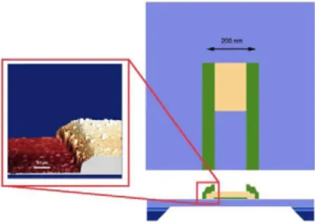
Fig. 1. Schematic layout (not to scale) of a lithographed bilayer showing top view of the device and a cross section through the central point. The AFM image shows the collapse of the overhanging Au, covering the Mo edges.
B. Bilayer Definition Through Lithography
After deposition, Mo/Au bilayers are patterned using stan-dard optical photolithographic techniques to get 200 x 200 ¡j,m and 300 x 300 ¡j,m detectors. First, the gold layer is etched using a KI/I solution through a photoresist mask. Later, the photoresist mask is removed by acetone and the Mo layer is etched in a H3PO4/HNO3/H2O2/DI solution. This solution is selective to Au, thus Au layer can be used as a mask for Mo. Moreover, since Mo etching is about 20 times faster in the lat-eral than in the vertical, Au layer overhangs Mo and, when sam-ples are taken out of the wet etch and let dry, these overhangs collapse covering in a simple way Mo edges [18], [19] as con-firmed by the AFM image shown in Fig. 1. This "normal metal" boundary condition has been proved to be a requirement for sharp and reproducible transitions [20], [21], since it eliminates edge effects and noise from quasiparticle and vortex fluctua-tions [22], [23].
After patterning Mo/Au bilayers, a superconducting path from the sensor to the bias circuit is deposited. Since thermal connection is controlled by the SÍ3N4 membrane, supercon-ducting materials are used to ensure good electrical conductiv-ity and thermal isolation. To simplify the fabrication process, in some cases Mo layer deposited at first place is also patterned into contact pads [24]. In our case, this simple idea is not feasible, since the wet Au etch also attacks Mo; thus, our approach consists on depositing an extra Mo layer of 175 nm thick by DC sputtering at a power of 35 W over a photoresist mask, leading to Mo pads after lift-off. A schematic layout of the final sensor is depicted in Fig. 1.
IV THERMOMETER CHARACTERIZATION
A. Functional Properties
0.015k
G
0C 0.01
i&'*'tñr*+*&!&A*¡
0.28 0.285 0.29 0.295 0.3 0.305 0.31
T(K)
Fig. 2. Example of a calculation for a Mo/Au lithographed bilayer (75 nm/ 215 nm). Dashed line correspond to the fit of R(T) measurements to (2). Inset: R(T)R(T) of Mo/Au bulk samples (solid symbols) and corresponding lithographed ones (empty symbols).
deposited on bulk substrates. This result contrast somehow with that reported by Olsen et al. [25]. The bilayer normal resistance is measured to be RN ~ 25 mO, similar to other TES sensors with equivalent normal metal thickness [21], [24].
The sensitivity of TES sensors, associated with the sharpness of their superconducting transitions is usually expressed by the logarithmic sensitivity, a, and written as follows:
dlogi? d\ogT
TdR
RdT (1)
In our particular case, the estimation of a by using (1) has associated a large error bar, which is mainly related to the sharp-ness of the superconducting transition and the noise in the R(T) measurement due to the small resistance values of our sensors. Therefore, to reduce the error bar in the a estimation and to determine in a more precise way how the bilayer sensitivity is increased by the lithography process, the following alternative analysis is performed: the critical temperature is estimated by linearly fitting the high temperature part of the superconducting transition, being Tc defined as the temperature at which the
linear fit and R(T) data diverge. For T < Tc, the R(T) curve
can be expressed as:
R(T) = RN exp T-Tc
AT (2)
where AT is the fitting parameter. Since for T < Tc, the R(T)
curve is expected to have a higher slope, a can be estimated as TC/AT, being this value temperature independent. By
fol-lowing this procedure it is found that the lithographic process increases a values from 220 to 600 ± 140. An example of this estimation is depicted in Fig. 2, where a = 600 ± 80 is obtained for a 75/215 nm lithographed Mo/Au bilayer.
To tune the bilayer Tc and to satisfy the requirements of the
final sensor residual resistance the normal metal layer thick-ness, ¿Au, is kept constant while changing the superconducting layer thickness, dMo- Fig. 3 displays R(T) curves normalized
to the residual resistance values for both lithographed and non lithographed bilayers. Solid symbols represent samples with
¿Au = 215 nm, while open symbols are used for bilayers
cov-ered by dAu = 115 nm. In order to illustrate the reproducibility of the bilayer fabrication process it is important to stand out that the temperature dependence of the resistance curve has
0.1 0.2 0.3 0.4 0.5
T(K)
Fig. 3. R(T) curves of some of the studied samples. Solid symbols represent samples with dAu = 215 nm, while empty symbols are used for bilayers covered by dAu = 1 1 5 nm.
been measured for bilayers which were deposited within a time interval larger than a year and the measured Tc dispersion was
lower than 20 mK.
The characteristics of our TES thermometers are deduced from previously presented data. Mo/Au TES with a working temperature ^100 mK, a transition width of ^ 3 mK, a ~ 600 and RN ~ 25 míí are achieved for bilayers formed by 53 nm of Mo and 215 nm of Au.
Moreover, as shown in Fig. 3, for the same dMo value, no
change in Tc is found when increasing dAu above the estimated
gold coherence length, £AU ~ 110-135 nm [26]. According
to Martinis et al. [22] Tc can be written as a function of
dMo, ¿Au and a parameter related to the interface
transpa-rency, t:
Tn=T( CO 1 1
do 1.13(1 + 1/6) t
1
do -kBTco\fns
dMnM
dsns
(3)
Since the Au thickness above £M does not influence the
Tc value, for d,Au > CM, we substitute dM = ÍM- Under this
assumption [26], the value of the transparency of the interface determined by fitting the Tc(dMo) data (not shown) to (3)—t ~
0.3—is similar to those reported for TES with excellent perfor-mance [14], [17], [18], [27].
Thus the deposition of a protective thin Au layer by sput-tering seems not only to ensure reproducibility and avoid Mo degradation, but also to provide a clear interface that increases coupling between the two layers, as pointed out by the high interface transparency. Moreover, RN can be tuned at wish,
depending on the requirements of each application, by changing the gold layer thickness, without affecting the other functional properties of the sensor.
B. Current to Voltage Characterization
0/
0 0.5 1 1.5 2
30mK 40 mK 50 mK 60 mK 70 mK 80 mK 85 mK 90 mK 95 mK
VTES (MV)
Fig. 4. IV curves at different bath temperatures. I T E S 1S the current through the TES and V T E S is the voltage across the device.
-n=3.43±0.03 - K=47.76±0.13nW/Kn
(3=1,067±0.004 nW/K
• Measured
• ^ ^ Fit
\
60 80 100 T ( m K )
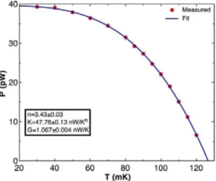
Fig. 5. Power plateaus in the transition as a function of bath temperature. Line represents the fit of measured data to P = K(TQ — Tf,a t^)n.
The power flow to the heat bath can be assumed to follow (4):
P = K-{Tn - T6™ bath) (4)
where the thermal conductance exponent, n, is a material dependent parameter, governed by the nature of the dominant thermal conduction process. On the contrary, K depends not only on the material properties, but also on its geometry, thus being completely different for every device, n and K parame-ters can be obtained by fitting the data displayed in Fig. 4 to (4), as shown in Fig. 5.
For this device the best fit was obtained using n = 3.43 and
K = 47.76 nW/(Kn). The n calculated value fully agrees with
those previously reported (3 < n < 4) [7], [12].
Finally, from the sensor parameters K and n an estimation of the thermal conductivity to the heat sink (G) can be obtained:
G = — - K • nT"-1
dTc c (5)
In our particular case a G value of 1.07 nW/K is estimated, which is in good agreement with other sensors with similar RN
and membrane thickness values [12], [28].
V. CONCLUSION
We have fabricated Mo/Au sensors at room temperature using UHV sputtering and e-beam deposition. These sensors are made of three layers: a sputtered Mo layer, a 15 nm
protective sputtered Au layer and an evaporated 200 nm Au layer. This extra Au layer, deposited by e-beam in a different chamber, is needed to obtain low values of RN as required for TES applications. The thin sputtered gold layer (15 nm) prevents Mo degradation, and provides good coupling between layers. A simple lithographic route is followed to achieve normal metal conditions on bilayer boundaries. Deposition over freestanding membranes instead of bulk substrates, and litho-graphic processes do not affect Mo/Au bilayers Tc; however,
and as expected, transition width is reduced, reaching a values ~600. Mo/Au TES parameters—Tc, RN, OÍ, n and G—display
values comparable to those found in literature for similar sensors [12], [20], [24], [28]. The excellent reproducibility, the sharpness of the transitions and the low residual resis-tance make these thermometers ideal for radiation detection applications.
ACKNOWLEDGMENT
The authors thank helpful discussions with people from the Netherlands Institute for Space Research (SRON), especially J. van de Kuur and L. Gottardi, and with J. M. Martinis.
REFERENCES
[1] A. T. Lee, P. L. Richards, S. W. Nam, B. Cabrera, and K. D. Irwin, "A superconducting bolometer with strong electrothermal feedback," Appl.
Phys. Lett., vol. 69, no. 12, pp. 1801-1803, 1996.
[2] M. J. Myers et al., "An antenna-coupled bolometer with an integrated micostrip bandpass filter," Appl. Phys. Lett., vol. 86, p. 114103, 2005. [3] M. D. Audley et al., "Scuba-2: A large-format TES array for
submillime-tre astronomy," Nucl. lustrum. Methods Phys. Res. A, Accel. Spectrom.
Detect. Assoc. Equip., vol. 520, no. 1-3, pp. 479-482, 2004.
[4] M. F. Cunningham et al., "High-resolution operation on frequency-multiplexed Transition-Edge photon sensors," Appl. Phys. Lett., vol. 81, no. 1, pp. 159-161, 2002.
[5] W. B. Doriese et al., "14 pixel, multiplexed array of gamma-ray mi-crocalorimeters with 47 eV energy resolution at 103 keV," Appl. Phys.
Lett., vol. 90, p. 193508, 2007.
[6] D. T. Chow et al., "Gamma-ray spectrometers using a bulk Sn absorber coupled to a Mo/Cu multilayer superconducting transition edge sensor,"
Nucl. Instrum. Methods Phys. Res. A, Accel. Spectrom. Detect. Assoc. Equip., vol. 444, no. 1/2, pp. 196-200, 2000.
[7] K. D. Irwin and G. C. Hilton, "Transition-Edge Sensors," in Cryogenic
Particle Detection, E. Christian, Ed. Berlin: Springer-Verlag, 2005,
pp. 63-149.
[8] M. Parra-Borderias et al., "Thermal stability of Mo/Au bilayers for TES applications," Supercond. Sci. Technol, vol. 25, p. 095001, 2012. [9] L. Fábrega etal, "Effects of stress and morphology on the resistivity and
critical temperature of room-temperature-sputtered Mo thin films," IEEE
Trans. Appl. Supercond., vol. 19, no. 6, pp. 3779-3785, 2009.
[10] R. González-Arrabal et al., "Mo/Au bilayers deposited by sputtering at room temperature for Transition Edge Sensors fabrication," J. Low Temp.
Phys., vol. 151, pp. 239-244, 2008.
[11] L. Fábrega et al., "Size and dimensionality effects in superconducting Mo thin films," Supercond. Sci. Technol, vol. 24, p. 075014, 2011.
[12] K. D. Irwin, G. C. Hilton, D. A. Wollman, and J. M. Martinis, "Thermal-response time of superconducting Transition-Edge microcalorimeters,"
J. Appl. Phys., vol. 83, no. 8, pp. 3978-3985, 1998.
[13] R. A. Matula, "Electrical resistivity of copper, gold, palladium, and sil-ver," J. Phys. Chem. Ref. Data, vol. 8, no. 4, pp. 1147-1298, 1979. [14] P. A. B. Toombs and P. Bennett, "Electrical resistance of thin
triode-sputtered gold films," J. Appl. Phys., vol. 39, no. 6, pp. 2948-2953, 1968. [15] M. Parra-Borderias, "Low Temperature Calorimetry Applications:
Radi-ation Detectors and Material CharacterizRadi-ation," Ph.D. dissertRadi-ation, Univ. de Zaragoza, Zaragoza, 2011, Colección de estudios de física, vol. 92, Prensas Universitarias de Zaragoza.
[17] L. Fábrega et al, "Mo-based proximity bilayers for TES: Microstructure and properties," IEEE Trans. Appl. Supercond., vol. 19, no. 3, pp. 460-464, 2009.
[18] T. C. Chen, F M. Finkbeiner, A. Bier, and B. DiCamillo, "Molybdenum-gold proximity bilayers as Transition Edge Sensors for microcalorimeters and bolometers," Supercond. Sci. Technol., vol. 12, no. 11, pp. 840-842, 1999.
[19] N. Tralshawala et al, "Fabrication of Mo/Au Transition-Edge sensors for X-ray spectrometry," IEEE Trans. Appl. Supercond., vol. 11, no. 1, pp. 755-758, 2001.
[20] G. C. Hilton et al., "Microfabricated Transition-Edge X-ray detectors,"
IEEE Trans. Appl. Supercond., vol. 11, no. 1, pp. 739-742, 2001.
[21] K. D. Irwin etal, "A Mo-Cu superconducting Transition-Edge microcalo-rimeter with 4.5 eV energy," Nucl. Instrum. Methods Phys. Res. A, Accel.
Spectrom. Detect. Assoc. Equip., vol. 444, pp. 184-187, 2000.
[22] J. M. Martinis, G. C. Hilton, K. D. Irwin, and D. A. Wollman, "Calculation on T c in a normal-superconductor bilayer using the microscopic-based Usadel theory," Nucl. Instrum. Methods Phys. Res. A, Accel. Spectrom.
Detect. Assoc. Equip., vol. 444, pp. 23-27, 2000.
[23] N. Tralshawala et al, "Design and fabrication of superconducting Tran-sition Edge X-ray calorimeters," Nucl. Instrum. Methods Phys. Res.
A, Accel. Spectrom. Detect. Assoc. Equip., vol. 444, pp. 188-191,
2000.
[24] J. A. Chervenak et al, "Fabrication of transition edge sensor X-ray microcalorimeters for constellation-X," Nucl. Instrum. Methods Phys.
Res. A, Accel. Spectrom. Detect. Assoc. Equip., vol. 520, pp. 460-462,
2004.
[25] J. E. Olsen et al, "Study of a Mo-Au TES deposited directly on a freestanding membrane," Nucl. Instrum. Methods Phys. Res. A, Accel.
Spectrom. Detect. Assoc. Equip., vol. 520, pp. 296-299, 2004.
[26] M. Parra-Borderias et al, "Proximity effect and interface transparency in Mo/Au bilayers for TES applications," submitted for publication. [27] R. Abusaidi et al, "Exclusion limits on the Wimp-nucl eon cross section
from the cryogenic dark matter search," Phys. Rev. Lett., vol. 84, no. 25, pp. 5699-5703, 2000.
[28] C. K. Stahle et al, "First results from Mo/Au transition-edge sensor X-ray calorimeters," Nucl. Instrum. Methods Phys. Res. A, Accel.