Si nanocrystals deposited by HFCVD
5
0
0
Texto completo
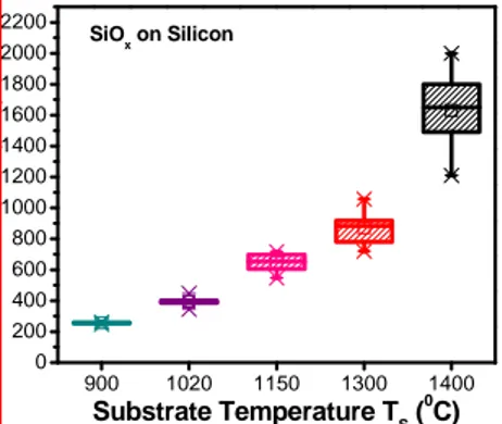
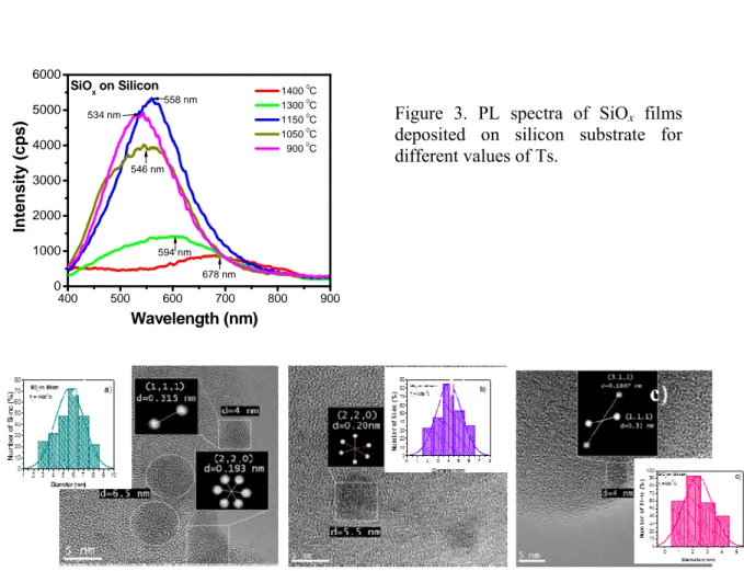
(2) 2. SCTE2012. the solid sources. In the HFCVD system a hot filament at ~ 2000 C dissociates the ultra-high purity molecular hydrogen that flows into the reactor at a rate of 50 sccm, producing atomic hydrogen. The filament-source distance was kept constant at 2 mm and the source-substrate distance was varied to change the Ts, and consequently to change the silicon excess in the SiOx films. The source-substrate distance was varied from 2 to 6 mm to change the substrate temperature from 1400 to 900 C, respectively. The films´ thicknesses were measured using a Dektak 150 profilometer. PL was measured at room temperature using a Horiba Jobin Yvon spectrometer FluroMax 3 with a pulsed xenon source and its detector has a multiplier tube. The samples were excited using light of 250 nm and PL response was recorded between 400 and 900 nm with resolution of 1 nm. Roomtemperature transmittance of the SiOx films was measured using an UV-Vis-NIR Cary 5000 system. The transmittance signal was collected from 190 to 1000 nm with a resolution of 0.5 nm. HRTEM measurements were done using a Titan 80-300 kV model with an energy spread of 0.8 eV. 2200 2000 1800 1600 1400 1200 1000 800 600 400 200 0. Results. Thickness (nm). SiOx on Silicon. 900. 1020. 1150. 1300. 1400. 0. Substrate Temperature TS ( C). Figure 1. Variation of the thickness of SiOx films as a function of Ts.. 80. 0. 1400 C 0 1300 C 0 1150 C 0 1020 C 0 900 C. SiOx on Quartz 2.5. 60. 2.4 2.3. Eg(eV). Transmittance %. 100. 40. 2.2 2.1 2.0 1.9. 20. 1.8 900. 1000. 1100. 1200. 1300. 1400 0. 0 200. Substrate Temperature Ts ( C). 400. 600. 800. 1000. Wavelength (nm). Figure 2. Transmittance spectra and energy band gap of SiOx films on quartz substrate as a function of Ts.. Figure 1 shows the thickness of the SiOx films as a function of the substrate temperature (Ts). It is observed that Ts clearly affects the thickness: thinner and more uniform SiOx films are obtained at lower temperatures. Such behaviour can be due to the temperature gradient in the HFCVD system; i. e., increasing the distance between solid source and substrate, the temperature gradient becomes smaller and this provides a more uniform deposit. Figure 2 shows the transmittance spectra of SiOx films on quartz substrate. The SiOx films exhibit a relatively high transmittance (>80%) between 600 and 1000 nm. The absorption edge shifts towards greater wavelengths as the substrate temperature increases. The corresponding optical band gap (Eg) values as a function of the substrate temperature are shown in the inset of Figure 2. Figure 3 shows the PL spectra from SiOx films deposited on silicon substrates. A wide PL spectrum, from 400 nm to 800 nm is observed for all the samples. PL spectra present a maximum emission peak centered between 534 and 678 nm depending of the Ts. A blue shift of the luminescent peak is observed when Ts decreases, coupled with an increasing of the emission intensity. The plan-view HRTEM micrographs of SiOx films deposited at 1150, 1020 and 900 °C are shown in Figures 4 a), b) and c), respectively. All micrographs show that the SiOx matrix contains small clusters, which, on the basis of the electron diffraction analysis, can be identified as silicon nanocrystals (Si-nc)..
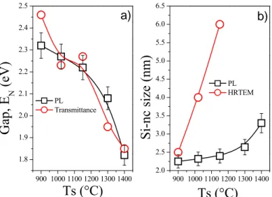
(3) 3. 6000. SiOx on Silicon. Intensity (cps). 5000. 0. 1400 C 0 1300 C 0 1150 C 0 1050 C 0 900 C. 558 nm. 534 nm. 4000. Figure 3. PL spectra of SiOx films deposited on silicon substrate for different values of Ts.. 546 nm. 3000 2000 1000. 594 nm 678 nm. 0 400. 500. 600. 700. 800. 900. Wavelength (nm). Analysis and Discussion PL properties of SiOx films have been studied extensively in the literature [1-2,13-14]. The two most accepted mechanisms of visible and near-infrared light emission for this type of materials are the quantum confinement effect in Si-ncs and another related with the role of defects around of the Si-ncs or defects in the SiOx matrix [1-14]. According to the first model, light emission from Si-ncs should be due to the band-to-band radiative recombination of electron-hole pairs confined within the crystals [15]. The second model attributes the PL of SiOx films to the presence of defects in the SiO2 matrix and/or to surface and interface effects of the Si-ncs and SiOx films [16-17]. According to our results, we have explored the possibility of the PL signals of the SiOx films studied is originated by the quantum confinement effect in the Si-ncs. So, the PL spectra (Figure 3) were analyzed in terms of a quantum confinement model more approximate to our results and more accepted [15,18]. In this model, the energy of the Si-nc gap, EN (eV) is defined as: (1) EN (eV ) 1240 / (nm) 1.12eV (3.73 / d 1.39 ) Where λ is wavelength of the Si-nc emission and d is the diameter of the Si-nc; thus the Si-nc diameter can be deduced as: 1. 3.73 1.39 d (nm) EN 1.12 . (2). Figure 5 a) and b) shows the results of applied equation (1) and (2), where is considerate only the values of the PL maximum peak () of Figure 3. These obtained values indicate a reduction of the crystal size and the enlargement of the Si-ncs band gap as the substrate temperature decreases.
(4) 4. SCTE2012. (black’s boxes). In the same Figure are shown experimental values of energy band-gap EN obtained by means of the transmittance spectra of SiOx films and using the Tauc´s law [19]. Also, are shown the size Si-nc obtained by HRTEM (red circles). The average sizes of the Si-ncs obtained with equation (2) have a value of 2.25 to 3.30 nm and they are different with respect at the experimental values of the Si-ncs obtained of HRTEM in the range from 2.5 to 6 nm as show in figure 5 b). The inset of Figure 4 shows the statistical analysis of the HRTEM images of the Si-ncs size distribution in the SiOx films. The Si-nc mean size is 2.5, 4 and 6 nm for SiOx films deposited at 900, 1020 and 1150 °C, respectively. These results obtained with equation (1) and (2) seem to be in agreement with the quantum confinement effect, which predicts the progressive blue-shift of the PL peaks with decreasing crystal size due to the enlargement of the Si-nc band gap. However, our results were calculated with equation (1) and (2) and only the peak of maximum PL value was considered, and not the others peaks of the PL spectra. These others PL peaks can to involve amorphous silicon (as Si-nps) and another related with the role of defects. Furthermore, the Si-ncs size obtained from HRTEM is very different respect with the obtained with equation (2). Therefore, this result experimentally not followed the quantum confinement effect. On the others hand, the origin of the PL bands between (400-700nm) is usually ascribed to different effects as: quantum dots, defects at the Si/SiO2 interface and defects associated with oxygen in the film. A detailed PL spectra study is on course and will be published. Therefore, it is possible that the substrate temperature produces another effects due at defects in the SiOx films such as: neutral charged oxygen vacancies (NOV) (Si-Si bonds), no bridging oxygen hole center (NBOHC), positively charged oxygen vacancies (E’ centres), interstitial oxygen molecules and peroxide radicals [7,8,10-12]. Some of these radiative defects such as NOV, and NBOHC can be activated with the Ts during the process, which can form Si-nps or E’ centres. 6.5. 2.5. a). 5.5. 2.2. 2.0. PL Transmittance. 1.9. Si-nc size (nm). Gap, EN (eV). 2.3. 2.1. b). 6.0. 2.4. 5.0 4.5 4.0. PL HRTEM. 3.5 3.0 2.5. 1.8. 2.0 900 1000 1100 1200 1300 1400. Ts (°C). 900 1000 1100 1200 1300 1400. Ts (°C). Figure 5. Experimental values of the a) Gap calculated of the equation (1) and Transmittance spectra, and b) Diameter of the Si-nc calculated of the equation (2) and HRTEM as a function of Ts. Conclusion. SiOx films deposited by HFCVD at different temperatures were studied. The results obtained of the equation (1) and (2) with the values of the PL maximum peak seem to be in agreement with the quantum confinement effect, which predicts the progressive blue-shift of the PL peaks with decreasing the Si-ncs size due to the enlargement of the Si-nc band gap. But, there are another PL peaks in the PL spectra that can to involve the role of the defects. Furthermore, the Si-ncs size by HRTEM and the gap energy of the Si-ncs obtained by transmittance spectra are different with these.
(5) 5. obtained with equation (1) and (2). Therefore and accordingly with these analysis, we proposed a combination of mechanisms to explain the photoluminescence in the films, where the dominant mechanism seem to be the quantum confinement effect in the Si-ncs with a contribution of the SiOx/Si defects. Acknowledgments. This work has been partially supported by CONACyT-154725 and VIEP-BUAP-2012. The authors acknowledge INAOE and CIQA laboratory for their help in the samples measurements. References [1] Iacona, F., Franzó, G. y Spinella, Correlation between luminescence and structural properties of Si nanocrystals, J. Appl. Phys., 87 (3), 1295, 2000. [2] Canham L. T., Journal Silicon quantum wire array fabrication by electrochemical and chemical dissolution of wafers. Appl. Phys. Lett., 57 (10), 1046, 1990. [3] Edelberg E., Bergh S., Naone R., Hall M and Aydil E., Luminescence from plasma deposited silicon films. J. Appl. Phys. 81 (5), 2410, 1997. [4] D. Dong et al, Preparation and some properties of chemically vapor-deposited Si-rich Si02 and Si.,Nq films J.Electrochem. Soc., 125, pp.819-823, 1978. [5] Y. C. Fang, W. Q. Li, L. J. Qi, L. Y. Li, Y. Y. Zhao, Z. J. Zhang, and M. Lu, Photoluminescence from SiOx thin films: effects of film thickness and annealing temperature, Nanotechnology, 15 (5), 494-500, 2004. [6]. L. Pavesi, L. Dal Negro, L. Mazzoleni, G. Franzo, and F. Priolo, Optical gain in silicon nanocrystals. Nature, 408, 440, 2000. [7] O. Hanaizumi, K. Ono, and Y. Ogawa, Blue-light emission from sputtered Si: SiO2 films without annealing. Appl. Phys. Lett, 82, 538-540, 2003. [8] Kohno, K.; Osaka, Y.; Toyomura, F.; Katayama, H. Jpn. Photoluminescence of Si Microcrystals Embedded in Si02 Glass Films. J. Appl. Phys., 33, 6616-6622, 1994. [9] P. G. Pai, S. S. Chao, and Y. Takagi, Infrared spectroscopic study of silicon oxide (SiOx) films produced by plasma enhanced chemical vapour deposition.J. Vac. Sci. Technol., A4, 689, 1986. [10] J. A. Luna-Lopez, M. Aceves-Mijares, O. Malik, Z. Yu, A. Morales, C. Dominguez and J. Rickards, Compositional and structural characterization of silicon nanoparticles embedded in silicon rich oxide Revista Mexicana de Física, S 53(7), 293, 2007. [11] J. A. Luna López, A. Morales-Sanchez, M. Aceves Mijares, Z. Yu, C. Dominguez, Analysis of surface roughness and its relationship with photoluminescence properties of silicon-rich oxide films. J. Vac. Sci. Technol. A 27(1), 2009. [12] J. A. Luna-López, G. García-Salgado, T. Díaz-Becerril, J. Carrillo López, D.E. Vázquez-Valerdi, H. JuárezSantiesteban, E. Rosendo-Andrés, A. Coyopol, FTIR, AFM, and PL properties of thin SiOx films deposited by HFCVD.Materials Science and Engineering, 174, 88– 92, 2010. [13] Jambois O., Rinnert H., Devaux X. and Vergnat M., Photoluminescence and electroluminescence of size-controlled silicon nanocrystallites embedded in SiO2 thin films J. Appl. Phys. 98, 046105-1, 2005. [14] Song H. Z., Bao M. X., Li N. S. and Zhang J. Y., Visible photoluminescence from silicon-ion-implanted SiO2 film and its multiple mechanisms. J. Appl. Phys. 82, 4028, 1997. [15] C. Delerue, G. Allan, and M. Lannoo, Theoretical aspects of the luminescence of porous silicon. Phys. Rev. B. 48, 11024, 1993. [16] L. N. Dinh, L. L. Chase, M. Baloch, W. J. Siekhaus, and F. Wooten, Optical properties of passivated Si nanocrystals and SiOx nanostructures, Phys. Rev. B, 54, 5029 1996. [17] T. Shimizu-Iwayama, N. Kurumado, D. E. Hole, and P. D. Townsend, Optical properties of silicon nanoclusters fabricated by ion implantation J. Appl. Phys. 83, 6018, 1998. [18] Gong-Ru Lin, Chun-Jung Lin, and Chi-Kuan Lin, Oxygen defect and Si nanocrystal dependent white-light and near-infrared electroluminescence of Si-implanted and plasma-enhanced chemical-vapor deposition-grown Si-rich SiO2 J. Appl. Phys. 97, 094306, 2005. [19] L.Wang, K Han, M. Tao, Effect of substrate Etching on Electrical Properties of Electrochemical Deposited CuO. J. Electrochem. Soc., 154, D91, 2007..
(6)
Figure
Documento similar
The main goal of this work is to extend the Hamilton-Jacobi theory to different geometric frameworks (reduction, Poisson, almost-Poisson, presymplectic...) and obtain new ways,
Astrometric and photometric star cata- logues derived from the ESA HIPPARCOS Space Astrometry Mission.
The photometry of the 236 238 objects detected in the reference images was grouped into the reference catalog (Table 3) 5 , which contains the object identifier, the right
In the previous sections we have shown how astronomical alignments and solar hierophanies – with a common interest in the solstices − were substantiated in the
Díaz Soto has raised the point about banning religious garb in the ―public space.‖ He states, ―for example, in most Spanish public Universities, there is a Catholic chapel
Keywords: iPSCs; induced pluripotent stem cells; clinics; clinical trial; drug screening; personalized medicine; regenerative medicine.. The Evolution of
In addition, precise distance determinations to Local Group galaxies enable the calibration of cosmological distance determination methods, such as supernovae,
Abstract: Transepidermal water-loss (TEWL), stratum-corneum hydration (SCH), erythema, elas- ticity, pH and melanin, are parameters of the epidermal barrier function and
