Blue and red electroluminescence of silicon rich oxide light emitting capacitors
7
0
0
Texto completo
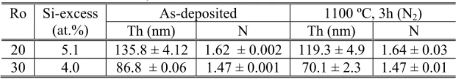
(2) In this work, the fabrication and study of simple light emitting capacitors (LECs) with active layers of LPCVD-SRO with two different Si concentrations is presented. Structural and photo emissive characteristics of the active material are verified in both as-deposited and thermally annealed films. The current density vs. electric field (J-E) behavior of the devices is studied paying special attention to changes in conduction states as the applied voltage is varied. Visible electroluminescence is obtained and its characteristics were studied for both R0 observing EL emission spectra differences with distinct Si-excess concentrations.. EXPERIMENT The SRO films were deposited on N-type silicon substrates ((100)-oriented) with resistivity of 5–10 Ω-cm by LPCVD using the flow ratio (Ro) between nitrous oxide (N2O) and silane (SiH4). Ro values of 20 and 30 were used for this experiment. Pilot samples were also deposited on N-type silicon substrates ((100)-oriented) with resistivity ≥2000 Ω-cm to study the composition (by Infrared spectroscopy) and the optical properties (PL) of SRO films. After deposition, SRO films were thermally annealed at 1100º C for 3 h in nitrogen atmosphere in order to induce the silicon agglomeration. The thickness and refractive index of the SRO films before and after annealing were measured with a Gaertner L117 ellipsometer (@632.8 nm). A ∼400 nm thick semitransparent n+ polycrystalline silicon (Poly) gate was then deposited onto the SRO film surface by LPCVD. After lithography processes step, square shaped gate of 4 mm2 area were defined. The backside contact was formed with 1 μm thick aluminum layer by evaporation. Infrared spectroscopy (BRUCKER Vector 22) was employed to study the composition of the SRO films. PL was carried out with the Fluoromax 3 spectrofluorometer from Horiba Jobin Yvon controlled by computer. The samples were excited using a 290 nm radiation and the emission signal was collected between 400 and 900 nm with a resolution of 2.5 nm. A cut-off filter to pass only wavelengths above 400 nm was used to block the light scattered from the source. Current–voltage (I–V) measurements were done with a computer-controlled Keithley 2400 source meter. The EL spectra were measured by biasing the devices with a constant DC voltage. Light emission was collected with an optical fiber which was located right onto the surface of devices and connected to a Fluoromax 3 spectrofluorometer from Horiba Jobin Yvon and analyzed with a computer. All measurements were done at room temperature.. RESULTS The thickness and refractive index of the as-deposited and annealed SRO films are reported in Table 1. As Ro value changes from 30 to 20, an increasing in the refractive index is observed, indicating the presence of silicon excess in the films. XPS studies on SRO films deposited under similar conditions showed that the SRO films contain 5.1 and 4.0 at.% of Si-excess for Ro = 20 and 30, respectively [2, 10]. Tabla 1. Thickness, refractive index and silicon excess of SRO films.. Ro 20 30. Si-excess (at.%) 5.1 4.0. As-deposited Th (nm) N 135.8 ± 4.12 1.62 ± 0.002 86.8 ± 0.06 1.47 ± 0.001. 1100 ºC, 3h (N2) Th (nm) N 119.3 ± 4.9 1.64 ± 0.03 70.1 ± 2.3 1.47 ± 0.01. Figure 1 exhibit the IR absorption spectra for the as-deposited and annealed SRO films. Both as-deposited and annealed films exhibit the typical features of the silicon dioxide, the absorption bands placed at about 457, 808 and 1056 cm-1 related to Si–O–Si rocking (peak 1), Si–O–Si bending (peak 2) and Si–O–Si stretching (peak 4), respectively [10, 11]. Nevertheless, an additional vibration band peaked at ∼885 cm-1 (peak 3) is observed for both as-deposited SRO films with Ro = 20 and 30 and it has been ascribed to HSi-O3 bending mode [12].This band disappears after the SRO films are thermally annealed, as observed in figure 1. A slight shift of the Si–O–Si stretching mode towards a higher wavenumber is observed when the Si-excess is decreased. Another shifting of the stretching mode is also observed after thermal annealing and it has been related with the phase separation of Si and SiO2 and thus the creation of Si-nps [2, 10, 11].. Proc. of SPIE Vol. 7719 77190N-2 Downloaded from SPIE Digital Library on 30 Jun 2010 to 158.109.6.183. Terms of Use: http://spiedl.org/terms.
(3) Figure 1. Infrared absorption spectra of SRO films before and after thermal annealing. Fig. 2 shows the PL spectra normalized to thickness for the as-deposited and annealed SRO films. As-deposited SRO films with 4 at.% of Si-excess exhibit an emission band with a maximum peak at ∼460 nm (B band) with a tail at longer wavelengths, as observed in figure 2(a). After thermal annealing, the intensity of this B band decreases and another PL band appears at ∼695 nm (A band) with stronger intensity. On the other hand, as-deposited SRO films with 5.1 at.% of Si-excess show a broad PL band from 410 to 860 nm with a maximum peak at ∼665 nm (A band), as observed in figure 2(b). This A band becomes stronger and slightly narrower after the thermal annealing is applied. A red-shift on the A band for SRO films with 5.1 at.% of Si-excess is also observed.. Figure 2. PL spectra for as-deposited and annealed SRO films with a) 4.0 and b) 5.1 at.% of silicon excess.. Proc. of SPIE Vol. 7719 77190N-3 Downloaded from SPIE Digital Library on 30 Jun 2010 to 158.109.6.183. Terms of Use: http://spiedl.org/terms.
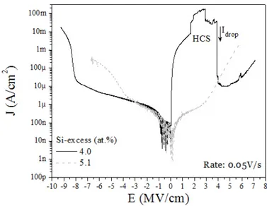
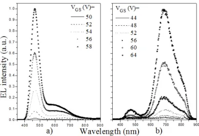
(4) Electrical and EL properties of SRO films were analyzed using simple MOS-like capacitors. Figure 3 exhibit the current density of fabricated devices as a function of the applied electric field (J-E). LECs with 4 at.% of silicon excess exhibit a high conduction state (HCS) at low voltages when they are forwardly biased (positive voltage applied to the gate respect to the substrate), as observed in figure 3. When a threshold voltage is reached, the current drops (Idrop) abruptly to ∼10 µA/cm2. This HCS and the current drop behavior have already been observed in devices with SRO-LPCVD films with the same silicon excess and it has been related to the annihilation of conductive paths created by adjacent stable Si-nps and unstable Si-nanoclusters (Si-ncls) [13]. After the current drops, subsequent I-V measurement exhibits a low conduction state at low voltages and the HCS is not observed (not shown). Afterwards, the current enters in a high electric field conduction regime. A clear increase in the current density that flows through the device is observed by increasing the Si concentration in the SRO layer, as observed by the dashed line in figure 3. The behavior of HCS in LECs with 5.1 at.% of Si-excess was not observed and it could be related to the presence of larger quantity of stable Si-nps than unstable Si-nlcs.. Figure 3. Typical I-V curve for LECs devices with annealed SRO films with 4.0 and 5.1 at.% of silicon excess.. Light emission in these LECs with both Si-excesses was observed when they were biased with a constant DC voltage. Figure 4 shows the EL spectra from both LECs at different applied voltages. Blue emission was observed in LEC devices with Si-excess of 4 at.% as shown in figure 4(a). The EL spectra for these devices exhibit a maximum peak at 466 nm with a tail at longer wavelengths. When the Si-excess in the LEC is increased to 5 at.%, the emission is shifted to the red-region, as observed in figure 4(b). EL spectra show the main emission at ∼685 nm, but an additional peak with low intensity is observed at about 470 nm. The EL intensity increases as the applied voltage is higher for both silicon excesses.. Proc. of SPIE Vol. 7719 77190N-4 Downloaded from SPIE Digital Library on 30 Jun 2010 to 158.109.6.183. Terms of Use: http://spiedl.org/terms.
(5) Figure 4. EL spectra for LEC devices with annealed SRO films with a) 4.0 and b) 5.1 at.% of silicon excess.. DISCUSSION Infrared studies on SRO films exhibited the typical features of the SiO2 films. The position of the Si–O–Si stretching mode at 1056 cm-1 for as-deposited SRO films is shifted if compared to the SiO2 at 1076 cm-1 and related to the presence of Si-excess in the films [2, 10, 11]. The stretching band of SRO films shifts to the SiO2 value after thermal annealing. This behaviour is well known to be related to a phase separation between Si and SiO2 and therefore the formation of Sinps [2, 10, 11]. The formation of Si-nps in annealed SRO-LPCVD films has been demonstrated in films deposited under the same conditions as the ones from this work [2, 11, 13]. Si-nps with an average size of 1.5 and 2.7 nm has been detected for annealed SRO films with 4 and 5.1 at.% of Si-excess, respectively. However, Si-nps have not been observed for as-deposited SRO films with these values of Si-excess. As-deposited SRO films with 4 at.% of Si-excess exhibit PL at the blue region (B band) with a tail at longer wavelengths. After annealing, this B band decreases and other PL band (A band) at the red-region appears with stronger intensity. The blue emission in SRO films has been associated with F and E defects (different types of oxygen vacancies), which are reduced or passivated after thermal annealing [14]. On the other hand, both as-deposited and annealed SRO films with 5.1 at.% of Si-excess exhibit a main peak emission at the red region (A band), which increases its intensity with the annealing. The A band emitted by these SRO films has been studied and related to the combination of Si-defects and Si-nps [1, 2, 10]. LEC devices with 4 at.% of Si-excess inside the SRO films show a HCS at low voltages which changes abruptly to a low conduction state when a threshold voltage is reached. The HCS is not observed anymore in subsequent measurements after the current drops abruptly. Similar I-V curves have already been observed in devices with SRO-LPCVD films with the same silicon excess [13]. The change of conductivity was analyzed and related to the annihilation of conductive paths created by adjacent stable Si-nps and unstable Si-ncls- and the creation of E’ defects. After the current drops and enters in a high electric field conduction regime at about 5MV/cm the LEC start to emit blue light. The light emission after the current drop phenomenon has already been observed in similar devices and has been attributed to an improvement in the carrier injection to reach radiative centers after preferential conductive paths are annihilated [9]. As the electric field is increased, the band bending is stronger thus more charges are injected to the SRO film and the EL emission becomes more intense. As observed in figure 2(a), a low intensity blue PL emission peak is still present after annealing. Then, E or F defects could be present after annealing. Therefore, the blue EL in LEC devices with 4 at.% of Si-excess could be related not only to E’ defects created after the current drops, but also by those which remain after the annealing. Nevertheless, studies need to be done to clarify this assumption. When the Si-excess is increased to 5.1 at.% in LEC devices, a larger current conduction is obtained at lower electric fields, as observed in figure 3. Therefore, EL in these devices is observed at a lower electric field (∼3.6MV/cm). These. Proc. of SPIE Vol. 7719 77190N-5 Downloaded from SPIE Digital Library on 30 Jun 2010 to 158.109.6.183. Terms of Use: http://spiedl.org/terms.
(6) devices emit at the red region, as observed in figure 4(b). The EL emission in these devices could be related to the presence of Si-nps and Si-defects such as the PL. The higher conduction in devices with high Si-excess is related to the presence of the luminescent centers in the SRO layer. E defects need higher electric fields to be excited compared with Si-nps in SRO films.. CONCLUSION PL and EL properties of SRO films with 4 and 5.1 at.% of silicon excess were studied. Blue and red PL is obtained in asdeposited SRO films depending on the Si-excess. While annealed SRO films exhibit a main emission band at the red region. Nevertheless, annealed SRO films with low Si-excess emit an additional PL band at the blue region but with low intensity. Blue and red EL was obtained with SRO films containing 4 and 5.1 at.% of Si-excess, respectively and using simple capacitive structures. LEC devices with SRO films as the active layer exhibit a higher current conduction as the Si-excess increases. Therefore a lower electric field was needed to obtain EL emission in devices with high Si-excess. Both blue PL and EL emission in SRO films were associated with F and E defects (different types of oxygen vacancies) meanwhile both red PL and EL were related to the combination of Si-defects and Si-nps.. ACKNOWLEDGMENT The authors acknowledge the support received from Consejo Nacional de Ciencia y Tecnología (CONACyT) and the Spanish Ministry of Science and Innovation (TEC2006-13907/MIC). The authors also thank Pablo Alarcón, Netzahualcoyotl Carlos, Mauro Landa and Manuel Escobar for their help in preparing the samples.. REFERENCES [1] Luna-López, J. A., Morales, A., Aceves, M., and Domínguez, C., "Analysis of surface roufghness and its relationship with photoluminescence properties of silicon-rich oxide films", J. Vac. Sci. Techol. A27(1), 57-62 (2009). [2] Morales, A., Domínguez, C., Barreto, J., Riera, M., Aceves, M., Luna, J. A., Yu, Z., and Kiebach, R., “Spectroscopical Analysis of Luminescence Silicon Rich Oxide Films”, Rev. Mex. Fís. S53(7), 279-282 (2007). [3] Flores Gracia, F., Aceves, M., Carrillo, J., Domínguez, C., and Falcony, C., “Photoluminescence and cathodoluminescence characteristics of SiO2 and SRO films implanted with Si”, Superficies y Vacío 18(2), 7-13 (2005). [4] Morales, A., Barreto, J., Domínguez, C., Riera, M., Aceves, M., and Carrillo, J., “Comparative study between silicon-rich oxide films obtained by LPCVD and PECVD”, Physica E 38(1-2), 54-58 (2007) [5] Buffet, N., Mur, P., De Salvo, B., and Semeria, M. N., “Silicon nano-crystals precipitation in a SiO2 matrix elaborated from the decomposition of LPCVD SiOx”, 2nd IEEE Conference on Nanotechnology, Proceedings, 269-272 (2002). [6] DiMaria, D. J., Kirtley, J. R., Pakulis, J., Dong, D. W., Kuan, D., Pesavento, F. L., Theis, T. N., Cutro, N., and Brorson S. D., “Electroluminescence studies in silicon dioxide films containing tiny silicon islands”, J. Appl. Phys. 56(2), 401-416 (1984). [7] Aceves, M., Falcony, C., Reynoso, A., Calleja, W., and Torres, A., “The conduction properties of the silicon /off–Stoichiometric SiO2 diode” Solid-State Electronics 39(5), 637-644 (1996). [8] Morales-Sánchez, A., Barreto, J., Domínguez, C., Aceves, M., Perálvarez, M., Garrido, B., and Luna-López, J. A., "DC and AC electroluminescence in silicon-nanoparticles embedded in silicon-rich oxide films”, Nanotechnology 21(8), 085710 (5 pp) (2010). [9] González Fernández, A. A., Aceves Mijares, M., Yu, Z., Morales Sánchez, A., and Leyva, K. M., "MOS like electroluminescent devices using silicon rich oxide obtained by LPCVD", 6th International Conference on Electrical Engineering Computing Science and Automatic Control (CCE2009) Proceedings, 611 (2009). [10] Morales-Sánchez, A., Barreto, J., Domínguez-Horna, C., Aceves-Mijares, M., and Luna-López, J. A., “Optical characterization of silicon rich oxide films” Sensors and Actuators A 142(1), 12-18 (2008). [11] Pai, P. G., Chao, S. S., and Takagi, Y., “Infrared spectroscopic study of SiOx films produced by plasma enhanced chemical vapor deposition”, J. Vac. Sci. Technol. A 4 (3), 689-694 (1986).. Proc. of SPIE Vol. 7719 77190N-6 Downloaded from SPIE Digital Library on 30 Jun 2010 to 158.109.6.183. Terms of Use: http://spiedl.org/terms.
(7) [12] Sassella, A., Borghesi, A., Corni, F., Monelli, A., Ottaviani, G., Tonini, R., Pivac, B., Bacchetta, M., and Zanotti, L., “Infrared study of Si-rich silicon oxide films deposited by plasma-enhanced chemical vapor deposition”, J. Vac. Sci. Technol. A 15 (2), 377-389 (1997). [13] Morales-Sánchez, A., Barreto, J., Domíınguez, C., Aceves, M., and Luna-López, J. A., “The mechanism of electrical annihilation of conductive paths and charge trapping in silicon-rich oxides”, Nanotechnology 20(4) 045201 (7pp) (2009).. Proc. of SPIE Vol. 7719 77190N-7 Downloaded from SPIE Digital Library on 30 Jun 2010 to 158.109.6.183. Terms of Use: http://spiedl.org/terms.
(8)
Figure

Documento similar
The host star peak intensity (blue line), the companion intensity (green line), the inverse of the averaged intensity in an area surrounding the central peak (red line) and
The emission at negative voltage for the nanocrystals, is reminiscent of that of the underlying NaCl template. The light intensity at positive polarity, with the tip over a
On the other hand at Alalakh Level VII and at Mari, which are the sites in the Semitic world with the closest affinities to Minoan Crete, the language used was Old Babylonian,
The detection technique is based on the identification of the blue WR bump (around He ii λ4686 Å, mainly associated with nitrogen-rich WR stars; WN) and the red WR bump (around C
This Raman image is colour-coded, where the intensity of the colour is correlated with the Raman intensity of three different bands: the A 1g mode of spinel Co 3 O 4 oxide (solid
Posteriorly, the same authors demonstrated that the incorporation of blue light at different doses (25–33%) into the light spectrum (combined with red and far-red, with a total PPFD
As in the case of pistachio, DIC treatment reduces band intensity as pressure and time increase, and the most effective treatment is DIC8 in which both the number and intensity of
On the other hand, significantly better scores at the end of the AM 6 program and after 6 months of follow-up as compared with baseline were observed in five subscales
