Classification of solar cells according to mechanisms of charge separation and charge collection
21
0
0
Texto completo
(2) 2. Introduction Understanding of solar cells until the 1990s was mainly based on two main models, the pn junction and the pin solar cell. The advent of nanostructured solar cells such as a dye-sensitized solar cell (DSC), bulk heterojunction organic solar cells (BHJ) or nanoparticle solar cells introduced a series of new device geometries. In some of these cases like the DSC, the electric field is of little relevance for charge collection at short circuit, while instead charge separation relies on interfacial kinetics, energy steps at interfaces and diffusion driven transport.1, 2 However, in some thin-film inorganic technologies the role of charge collection by electric fields is essential to the solar cell performance.3 The general energetic picture of solar cells is a very important tool for the understanding of the role of the different materials and interfaces, the electronic processes, and the interpretation of many characterization techniques. Currently, we are witnessing the birth of a new solar cell technology, namely organic-inorganic halide perovskites whose efficiencies have risen to exceed 20 % faster than any other solar cell technology before.4-9 To further optimize these perovskite solar cells, it will be crucial to understand their physical and electrical characteristics which are currently discussed.10, 11 Here we propose a general discussion that gathers the knowledge obtained in the last decade for the description of solar cells in terms of a macroscopic energy diagram that may put future new candidates for photovoltaic energy conversion in a firm classification. The general solar cell structure described here is composed of one central layer that contains the absorber material, and two extracting contacts. Photovoltaic conversion is based on interfering effectively with the process of recombination that restores thermal equilibrium by de-excitation of electrons in the conduction band. Thus non-equilibrium carriers must be extracted before they recombine, so that the charge collection efficiency is large. The first step to achieve such goal is an effective separation of the electron hole pair, formed by the excitation dipole, at the site of the photogeneration event. Then, the central layer must realize the function of effective transport of electrons and holes from the point of generation to their respective contacts. Note that the central layer may consist of a single material that absorbs photons and transports both electrons and holes effectively, as in silicon and polycrystalline inorganic solar cells. Otherwise the active layer may be formed by a combination of materials, as in a DSC where the absorber is a monolayer of dye that is locally sandwiched between nanostructured electron and hole conductors. Although local differences of energy exist, to facilitate charge separation, the central layer is viewed as a macrohomogeneous medium in which only the macroscopic electrical field perpendicular to the contact is relevant to the transport and collection of each kind of carrier.12 In these types of nanocomposite solar cells, the conduction band and valence band shown in the diagram correspond to different materials, those that transport electrons and holes, respectively, while the initial kinetics of charge separation are not represented in the diagram. Finally, overall charge separation and collection requires photovoltaic devices to have one built-in asymmetry.
(3) 3. that ensures that charge carriers with different polarity are collected at different contacts so that a net current flow becomes possible. In the following discussions, we will summarize the mechanisms whereby these functions are achieved for the main types of solar cell devices.. Charge separation Effective local charge separation is an essential feature to avoid immediate, geminate recombination of individually photogenerated electron-hole pairs in low permittivity absorbers and/or at low temperatures. Charge separation means that bound states like excitons that may be formed initially after photogeneration dissociate to form two separate unbound charge carriers of opposite polarity. After the initial separation of the geminate pair, so-called non-geminate recombination may occur between electrons in the conduction and holes in the valence band. Specific mechanisms of charge separation may differ broadly depending on the type of absorber and its relative permittivity. In homogeneous semiconductors such as standard inorganic thin films or c-Si with relatively high dielectric permittivities and low exciton binding energies, local charge separation is very efficient at least at room temperature without the assistance of electrical fields. Thus, each photogenerated carrier rapidly forms part of the respective ensemble of free carriers in the conduction or valence band (after a carrier thermalization time).13 Also in CH3NH3PbI3 perovskite solar cells, the exciton population at room temperature seems to be negligible.14, 15 The photogenerated carriers are separated on ps time scale and the radiative recombination occurs between uncorrelated electron-hole carriers rather than geminate pairs.16 A common misconception is that the pn junction is crucial for and/or the main locus of charge separation in inorganic solar cells.17 The pn junction occupies a very small region in a c-Si solar cell as explained below, and its purpose is to provide a carrier selective junction that makes sure that carriers with different polarities diffuse to different junctions..
(4) 4. Fig.1. Charge separation and transport in a dye-sensitized solar cell. Electrons are injected from the excited state of a sensitizer to the TiO2 framework, and they travel by diffusion across the semiconductor until collected at the transparent conducting oxide (TCO) substrate. Holes in the ground state of the absorber are ejected to a hole transport medium. Holes are prevented to enter the electron collecting TCO by a blocking layer, and they are accepted at the counterelectrode (CE). The separation of Fermi levels of electrons ( E Fn ) and holes ( E Fp ) produces a photovoltage. On the other extreme of the architectures of absorbers we find those cells in which the absorber is a single isolated molecule, or a nanocrystalline fragment of material as a semiconductor quantum dot (QD). The paradigm of this type is a DSC.18 As schematically shown in Fig. 1, the sensitizer lies between an electron transport medium (nanostructured TiO2) and a hole transport layer (either redox electrolyte or solid hole conductor). Initial charge separation in this system is achieved by suitably arranged preferential injection kinetics to either electron or hole transport medium. In this process any role of band bending or local pn junction can be safely ignored, as the size of the absorber is too small to sustain an energy barrier due to band bending. But in this type of absorber, charge extraction competes with internal recombination of the electron hole pair. Therefore it is important to facilitate fast extraction by a good match of the energy levels in both media involved and by ensuring the existence of downhill energy pathways from the light absorber to the carrier transport material. It is also required that the kinetic and energetic charge transfer pathways prevent the return of injected carrier to the original absorber molecule. In natural photosynthesis energy harvesters, the use of a relay of redox molecules to achieve a large physical separation of the electron and hole is a basic strategy to avoid recombination. Deleterious backward energy transfer of a separated electron hole pair is also prevented by placing such process energetically in the Marcus inverted region.19 Similarly in bulk heterojunction solar cells, rapid electron transfer occurs between the organic light absorber (electron donor) and organic electron transporter (electron acceptor), usually a functionalized fullerene. Recombination of the primary electron-hole pair is usually not an issue in DSCs, mainly because the metal-organic light absorbers are designed to have an orbital or molecular structure that internally favours charge separation and electron injection to TiO2.20 There occurs an energy loss at this step, which is rather significant at the contact of the dye with the redox couple in a DSC. In fact, the effective band gap of the solar cell is reduced to the difference of energy levels between electron and hole transport materials. In a BHJ solar cell the effective bandgap at the donor-acceptor interface is termed the charge transfer state energy.21 In some metal-free organic dyes used in DSC the extent of internal recombination becomes a concern,22 and much more so when the absorber is an inorganic QD, which displays complex internal electronic dynamics, often governed by recombination at surface states. Effective passivation of the QD absorber greatly improves the internal quantum efficiency (IQE) in QD sensitized solar.
(5) 5. cells.23. Charge collection Once the initial charge separation step is achieved, it is necessary to establish a flux of both types of carriers towards separate contacts. The solar cell must have a built-in asymmetry, so that each external contact injects and extracts ideally only one carrier. Therefore the contacts must be selective to a specific carrier, which can be achieved in a number of ways. In the end, the voltage in a solar cell is given by the difference of the quasi-Fermi level of electrons at the electron selective contact, to the quasi-Fermi level of holes at the hole selective contact.1, 24 In all solar cells a certain thickness of the absorber layer, d , is required to effectively absorb all solar photons. The desired range of values of d is determined by the absorption coefficient and light scattering properties of the device that increase the optical pathlength of weakly absorbed photons in the absorber. On their way to the contacts, electrons and holes encounter each other in the central layer, which can lead to recombination events that are quantified, in a generic sense, by a recombination lifetime . This lifetime may depend on impurities, dislocations and grain boundaries in inorganic solar cells or on the local microstructure of donor-acceptor network in organic solar cells. The selectivity of contacts must be combined with the need for charge extraction at a rate faster than charge recombination, and the specific mechanisms achieving this will be now discussed in some detail. We start with the representative situation of a DSC, in which the diffusion length Ldiff is large, so there is a large probability to collect each photogenerated electron at the contact, and indeed the internal quantum efficiency IQE 1 .25 In the standard, liquid electrolyte case, the concentration of ionic charge carriers is very large, and the voltage is produced by the rise of the electron quasi-Fermi level, as shown in Fig. 2b and c. This diagram is also fairly representative of the operation of crystalline silicon solar cells. As shown in Fig. 1, in a DSC no specific directionality to transport exists in the direction perpendicular to the outer contacts. Both electrons and holes may diffuse either way. However, holes cannot be injected into the electron collecting TCO layer, due to the presence of a blocking layer. On the other hand electrons are stopped at the end of the TiO2 layer that is separated from the counter electrode. In this type of cell, charge carrier selectivity is achieved in all internal electronic processes using materials and morphologies that provide an easy pathway for one carrier and a large barrier to the other one. Similarly extended use of blocking layers is made in organic solar cells and in organic light emitting diodes (OLEDs).26 In the case of c-Si charge carrier selectivity is attained by the use of a thin (in comparison with the central layer) pn junction..
(6) 6. a. 10. OPV CdTe a-Si. CIGS. c-Si DSC -3. 10. b EC. w Ef. -2. d EC. 10. V=0. V=0. EV d. Efn. -1. V = Voc. Efp. Efn. EC. EV d. e. 0. f. w. V=0. EV. c. 10. typical ratio w/d. V = Voc. d=w. g Efp. Efn. V = Voc. Efp. Fig. 2. a The typical ratio of space charge region width w and thickness d for different solar cell technologies. Band diagrams of solar cells with small w/d (b, c), intermediate w/d (d, e) and w=d (f, g) at short circuit in the dark (b, d, f) and open circuit (c, e, g). The grey areas represent the main space charge regions in the different diagrams at short circuit. Characteristically, the selective contacts are represented by materials that themselves are n- or p-type. However, selective contacts may be formed by materials that have the required kinetic properties to extract only one kind of carrier at the interface with the absorber. Kinetic selectivity, by appropriate match of energy levels at the interface, is therefore a fundamental resource available for energy conversion devices. It is not generally required that the material that extracts holes is a hole-only conductor. One example is MoO3 that has a very large work function and is strongly n-type by the presence of oxygen vacancies, but it nonetheless forms an excellent selective contact to holes in organic devices, due to the existence of a large interfacial dipole.27, 28 In OLEDs, tuning the energy level of the cathode to the organic active layer has also been achieved by interfacial dipole layers that reduce the effective work function of a metal such as Al.29, 30 In QD films, it has been shown that a change of contact extraction properties can invert the photovoltage, even when all electrical fields are shielded by immersion in an electrolyte.31 Another significant aspect of the solar cell interface contacts is that they may constitute an important locus for unwanted recombination. To prevent the carrier loss in silicon solar cells a back surface field is formed that reflects the majority carrier, or a passivation layer is introduced that may be made up of materials like SiO2, amorphous Si or Al2O3.32, 33 These treatments provide significant gains of photovoltaic power conversion efficiency. In perovskite solar cells, important differences of recombination affecting device performance have been determined depending on the contact materials..
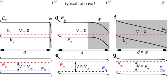
(7) 7. 34. However, in general, the selective contact to electrons must be ohmic and form a small injection barrier for electrons. Thus, materials with a low work function are required. These will then align well to the conduction band minimum energy level of the absorber layer. Oppositely, materials with a large work function may form an efficient hole extraction contact. In consequence all solar cell devices contain an intrinsic built-in potential between the outer contacts. In some cases the built-in field does not help (much) with charge extraction at short circuit. This is typically the case when the builtin field is confined to a narrow space charge region or to a dipole layer (as in c-Si and DSC respectively). Nevertheless, the built-in voltage Vbi ensures that the applied forward bias V (e.g. at the maximum power point of an illuminated solar cell) can drop somewhere. As long as Vbi – V is still positive no barriers for extraction will form.3, 35, 36 Thus, the built-in voltage serves an important role even if like in c-Si solar cells, charge collection is nearly entirely driven by diffusion. Alternatively, the built-in field, obtained after initial device formation, may be extended over the absorber thickness and take a leading role in charge extraction. In fact the device might be even fully depleted at short circuit in which case, the built-in electric field extends over the whole absorber, as in amorphous silicon solar cells, Fig. 2f and g.37 Intermediate situations can exist, Fig. 2d and e, as in the case of organic bulk-heterojunctions where both band bending in the absorber and contact dipole account for the total Vbi.38 In some organic solar cells a low flat band voltage 0.4 V has been measured implying that the field-free neutral region comprises nearly the whole absorber thickness at voltages much below the maximum power point.39 Recent studies of the energy diagram of CH3NH3PbI3 perovskite solar cells show a large builtin voltage and significant electrical field in the absorber region.40 In order to classify solar cell types with regard to their way of separating charge carriers, a useful criterion is therefore the ratio between the width w of the space charge region and the absorber thickness d.41 Figure 2a compares important solar cell technologies in terms of their ratio w/d. Crystalline Si (c-Si) as well as DSCs are typical examples of solar cells that have a tiny space charge region relative to the total absorber width. Figure 2b shows the band diagram of a p-type semiconductor at short circuit in the dark. The doping is sufficiently high relative to the absorber thickness that w/d << 1. Here, electron transport through the device will be mostly by diffusion as already explained above. For typical inorganic thin film solar cells, the ratio w/d varies from around 1/10 in Cu(In,Ga)Se2 (CIGS) to 1 in fully depleted devices like amorphous or microcrystalline Si (a-Si or c-Si). Figures 2d-g show the schematic band diagrams for devices with intermediate (d, e) and high (f, g) ratios of w/d. When going from small to large values of w/d, the way charge separation happens in the solar cell changes. While devices with low w/d are controlled by diffusion such as in the case of c-Si and DSC, the larger the space charge region becomes relative to the absorber thickness, the more drift will affect.
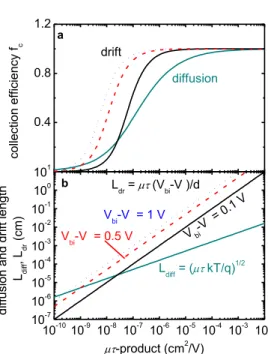
(8) 8. charge carrier collection. One obvious way to improve charge carrier collection is to improve the mobilitylifetime product e.g. by improving microstructure of the material, by reducing the defect density or by increasing the grain size. While mobility and lifetime have a huge influence on charge carrier collection, the pathways to improvement are material specific. However, in order to decide which ratio w/d is best for efficient charge collection, we can make quite general statements if we decide to use a level of abstraction where the absorber material is essentially just described by a mobility, a lifetime and a doping density. Whether it is better to use a geometry that is mostly depleted at short circuit (high w/d like in amorphous Si) or a geometry where the electric field F only drops in the periphery of the device (low w/d ) depends mostly on the mobility-lifetime product of the material and how that depends on doping density. For a wide range of mobility ()lifetime () products, the collection efficiency for charge carriers at short circuit is improved if transport is due to drift rather than diffusion as shown in Fig. 3a. This is due to the fact that at normal operating conditions of thin-film solar cells the diffusion length Ldiff kT / q of charge carriers is typically smaller than the drift length Ldr F as shown in Fig. 3b. Only for very low values of , Ldiff > Ldr due to the square rootlike dependence of Ldiff on increasing initially faster than the linear dependence of Ldr on . However, this is only relevant for collection efficiencies that are too low to allow efficient solar cells. collection efficiency fc. 1.2. a. drift 0.8. diffusion. 0.4. diffusion and drift length Ldiff, Ldr (cm). 1. 10 0 b 10 -1. 10 -2 10 -3. 10 -4 10 -5 10. Ldr = (Vbi-V )/d Vbi-V = 1 V. Vbi-V = 0.5 V. -V V bi. V .1 =0. Ldiff = (kT/q). 1/2. -6. 10 -7 10 -10 -9 -8 -7 -6 -5 -4 -3 -2 10 10 10 10 10 10 10 10 10 2 -product (cm /V). Fig. 3: The collection efficiency (a) of charge carriers depends strongly on the mobility lifetime product and the electric field. For a wide range of -products, the drift length is longer than the diffusion length (b) and therefore charge carrier collection is improved by an electric field. The main reason not to choose a pin-junction for all devices is that it is disadvantageous for the open-circuit voltage. Thickness used for the.
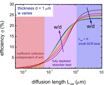
(9) 9. calculation of the average electric field is d = 1 µm. So far, we have shown that there are different ways of implementing carrier selectivity and that the electric field usually helps extracting charges at short circuit. However, towards open circuit, the electric field naturally gets smaller with the effective built in voltage Vbi,eff = Vbi – V decreasing linearly with applied forward bias. This means that the field assisted collection will always be worse at the maximum power point relative to short circuit and the fill factor of cells that rely on drift to collect charges will be reduced relative to those that rely mainly on diffusion. But nevertheless in Fig. 3 we have shown that even at an effective built-in voltage as low as 100 mV, collection via drift is usually still better than diffusion for relevant values of the collection efficiency. Thus, the question is warranted whether there are any situations where one would want the ratio w/d to be small rather than large. Indeed it is desirable to have w/d to be small in cases, where collection is efficient even by diffusion, because of the increased recombination losses at open circuit in devices with large space charge regions. In nearly all solar cell technologies, deep traps, situated close to the center of the gap, dominate recombination. For these deep traps, recombination is usually modelled using Shockley-Read-Hall (SRH) statistics. The SRH recombination rate has a maximum where nn=pp, where n,p are the capture cross sections for electrons and holes, respectively. In the neutral region of a crystalline Si pn-junction solar cell, the minority carrier concentration is much smaller than the majority carrier concentration under normal operating conditions and so the SRH recombination is much smaller than in the space charge region where photogenerated n ≈ p. Thus in a c-Si solar cell with its large diffusion length it is certainly advantageous to minimize the region in which n ≈ p. Figure 4 sums up all effects of charge carrier collection and recombination and shows how, for a particular case, the efficiency depends on the ratio of w/d, controlled by changing the doping density, and on the diffusion length, controlled by changing the mobility. The result is that for Ldiff > d, the device should ideally have a small space charge region and a large field free region as in c-Si. For Ldiff < d, we distinguish two regimes. The first regime for higher -products represents the range where the drift length is still high enough to allow charge extraction in the space charge region. Therefore, it is advantageous in this case to have a fully depleted device (doping as low as possible). For very low -products, diffusion becomes more efficient than drift as seen already in Fig. 3. However in this case, collection is so inefficient that this regime has no practical relevance. Note that while Fig. 4 is simulated for a device with a thickness of 1 µm, the fundamental trends stay the same when the thickness is changed. In the supporting information, we present simulations for the case of a 150 nm absorber, which is more representative for organic solar cells..
(10) 10. 30. efficiency (%). thickness d = 1 m 25 w varies 20. w/d. w/d. 15. Ldiff > d : small SCR best. 10 5. inefficient collection independent of w/d fully depleted absorber best -2. 10. -1. 10. 0. 10. 1. 10. diffusion length Ldiff (m) Fig. 4: Simulated efficiency vs. diffusion length for different values of the doping density leading to different ratios w/d. For Ldiff > d, efficiency increases for smaller space charge regions because of the loss in Voc and FF. For Ldiff < d, the absorber should ideally be fully depleted because charge extraction is more efficient if assisted by drift. For very low diffusion length, this situation changes again to the case for Ldiff > d, however, due to the overall low collection efficiency this is of no relevance for practical solar cells.. Ferroelectric photovoltaic effects The surge of organic-metal-halide perovskites has brought the attention of the scientific community towards physical effects that were not previously considered in the analysis of mainstream types of solar cells. These physical factors may produce PV mechanisms that lie outside those described in the previous sections. For example the observation of a very large increase of the low frequency dielectric constant 11 in CH3NH3PbI3 solar cells and very slow reorganization phenomena42 are difficult to explain on the basis of electronic phenomena alone and appears to involve some structural modification. Here we describe briefly the ferroelectric effect and in the next section the photoinduced changes of ionic concentration. The PV effect in ferroelectric materials depends on the polarization-induced internal electric field. For 50 years it is known that ferroelectric perovskites may produce a large photovoltage exceeding by far the bandgap of the absorber material43, 44 but the principles that cause the observed response are not fully understood yet. Most metal oxide perovskites with ferroelectric properties are unsuitable to harvest of the solar spectral photons, as they have a large bandgap of 3-4 eV, but recently perovskites with band gaps closer to the required 1 - 1.5 eV have been synthesized. These materials have suitable optical and electronic properties for a PV absorber material.45-47 One route for.
(11) 11. the exploitation of perovskite materials in PV applications starts from inorganic perovskites that show internal enhanced electrical fields due to the ferroelectric effect. The larger than bandgap photovoltages cannot be explained by the regular mechanism of separation of Fermi levels in a homogeneous absorber layer. One assumption to explain these phenomena relies on a local disposition of electric fields formed by spontaneous polarization over short distances of a few nm. This structure causes local steps of builtin potential as suggested by recent observations of domain wall structure at the nanoscale.48 The local variations in electrostatic potential in these materials might cause a situation similar to that observed in multijunction solar cells, where regions with high recombination work as tunnel junctions. The voltage of regions between the tunnel junctions then adds up, while the photocurrent is limited to that of one region. One difference between the behavior of multijunction solar cells and the situation in BiFeO3 is that the current voltage curve in the latter is typically ohmic and not diode-like, which is probably explained by the low conductivity of BiFeO3. Until recently, these PV materials produced negligible photocurrents and ohmic characteristic with small fill factor. A major breakthrough in this field was the demonstration of multiferroic oxide solar cells based on double perovskite thin film Bi2FeCrO6.49 A control of long range ordering of the cationic components of the perovskite, Fe and Cr, reduces the optical absorption edge to 1.5 eV, by introducing charge transfer excitations between Fe and Cr. By fabrication of multilayer structures with a graded bandgap the photocurrent increases to 20 mA cm-2, giving the PCE of 8.1% which is competitive with other starting technologies.. Effect of ion movement on photovoltage Junctions and doping profiles in most solar cell materials are usually considered to be static with respect to changes in electric field. However, in some cases drift of charged defects or ions can change the doping profile and therefore the electric field distribution in a solar cell. In general a voltage is defined as the difference of electrochemical potential of electrons between the contacts, and such voltage may arise either from the variation of chemical potential of electrons and holes (as shown in Fig. 1 and 2), from a change of the chemical potential of ions, or from a combination of both.13 In mixed ionelectron conducting cells50 a part of the cell voltage may be due to the ionic component. We are familiar with Li ion electrochemical cells that produce changes of voltage due to the variation of the chemical potential of the lithium ions.51 In electronic insulators that are good ionic conductors, such as ion conducting glasses, external electrical polarization induces a displacement of ionic charge that may form depletion layers near the contact, totally ionic in origin (in contrast to the familiar electronic Schottky barrier in usual solar cells).52 In a liquid electrolyte DSC it is obvious that ionic displacement occurs to compensate electronic charge injected in the nanostructured TiO2 framework for restoring electroneutrality. In solid state DSC with 2,2′,7,7′-tetrakis(N,N-di-pmethoxyphenyl-amine)9,9′-spirobifluorene (spiro-OMeTAD) hole conductor, the.
(12) 12. displacement of ions cause strong transient effects until an electroneutral distribution is achieved.53 However, ionic components of the photovoltage have not been considered in the DSC area, since concentration of the supporting ions is usually very large and the variation of redox ions is negligible. Recently it has been suggested that facile migration of ions occurs in CH3NH3PbI3 perovskite solar cells.54, 55 The chemical potentials of Pb+ and I- defects and interstitials have been mapped and the domain of structural stability has been predicted by computation.56 Under photogeneration of carriers, a drift of ionic defects may establish an ionic gradient by accumulation at one contact and scarcity at the opposite contact side. Then one can move from a situation with two contacts with similar work functions to a situation where you have a pn or np junction that leads to a good photovoltage. This topic is currently under active investigation.. Conclusions The operation of solar cells relies on local mechanisms for charge separation that may consist on the fast transfer of photogenerated carriers to different media, or simply lead to the presence of both electrons and holes distributed in the same medium. In either case the transport to the contacts must compete against recombination, and the distribution of the electric field inside the solar cell has a profound impact on charge carrier collection. A classification in terms of the ratio between diffusion length and space charge width is provided observing that there is no general optimum working mechanism in terms of space charge width w. Depending on the diffusion length, there are different optimum conditions. For high diffusion lengths (Ldiff >d), a small space charge width will typically improve photovoltaic efficiency because it improves the open-circuit voltage. If the diffusion length is up to roughly an order of magnitude smaller than the cell thickness, a fully depleted solar cell will usually improve charge carrier collection and therefore the efficiency. Thus, for every new solar cell technology the band diagram including the electric field distribution needs to be measured and taken into account as a design criterion for further photovoltaic optimization.. Acknowledgments This work was supported by MINECO of Spain under project MAT2013-47192-C31-R), and the Helmholtz-Energy-Alliance “Hybrid-Photovoltaics”..
(13) 13. References 1. J. Bisquert, D. Cahen, S. Rühle, G. Hodes and A. Zaban, The Journal of Physical Chemistry B, 2004, 108, 8106-8118. 2. P. Würfel, Physics of Solar Cells. From Principles to New Concepts, Wiley, Weinheim, 2005. 3. T. Kirchartz and U. Rau, in Advanced Characterization Techniques for Thin Film Solar Cells, eds. D. Abou-Ras, T. Kirchartz and U. Rau, Wiley, Berlin, 2011, p. 14. 4. H. Zhou, Q. Chen, G. Li, S. Luo, T.-b. Song, H.-S. Duan, Z. Hong, J. You, Y. Liu and Y. Yang, Science, 2014, 345, 542-546. 5. M. Liu, M. B. Johnston and H. J. Snaith, Nature, 2013, 501, 395-398. 6. A. Kojima, K. Teshima, Y. Shirai and T. Miyasaka, Journal of the American Chemical Society, 2009, 131, 6050-6051. 7. J. Burschka, N. Pellet, S.-J. Moon, R. Humphry-Baker, P. Gao, M. K. Nazeeruddin and M. Grätzel, Nature, 2013, 499, 316-320. 8. H.-S. Kim, S. H. Im and N.-G. Park, The Journal of Physical Chemistry C, 2014, 118, 5615–5625. 9. N. J. Jeon, J. H. Noh, Y. C. Kim, W. S. Yang, S. Ryu and S. I. Seok, Nat Mater, 2014, 13, 897-903. 10. S. A. Bretschneider, J. Weickert, J. A. Dorman and L. Schmidt-Mende, APL Materials, 2014, 2, 040701. 11. E. J. Juarez-Perez, R. S. Sanchez, L. Badia, G. Garcia-Belmonte, V. GonzalezPedro, Y. S. Kang, I. Mora-Sero and J. Bisquert, The Journal of Physical Chemistry Letters, 2014, 5, 2390−2394. 12. A. Gagliardi, M. Auf der Maur, D. Gentilini, F. di Fonzo, A. Abrusci, H. J. Snaith, G. Divitini, C. Ducati and A. Di Carlo, Nanoscale, 2015, 7, 1136-1144. 13. J. Bisquert, Nanostructured Energy Devices: Equilibrium Concepts and Kinetics, CRC Press, Boca Raton, 2014. 14. J. S. Manser and P. V. Kamat, Nat Photon, 2014, 8, 737-743. 15. Y. Yamada, T. Nakamura, M. Endo, A. Wakamiya and Y. Kanemitsu, Journal of the American Chemical Society, 2014, 136, 11610-11613. 16. K. Chen, A. J. Barker, F. L. C. Morgan, J. E. Halpert and J. M. Hodgkiss, The Journal of Physical Chemistry Letters, 2014, DOI: 10.1021/jz502528c, 153-158. 17. X. Y. Zhu, The Journal of Physical Chemistry Letters, 2014, DOI: 10.1021/jz5008438, 2283-2288. 18. B. O'Regan and M. Grätzel, Nature, 1991, 353, 737-740. 19. J. R. Durrant, S. A. Haque and E. Palomares, Chemical Communications, 2006,.
(14) 14. DOI: 10.1039/b601785c, 3279-3289. 20. M. Pastore and F. de Angelis, Journal of Physical Chemistry Letters, 2013, 4, 956-974. 21. K. R. Graham, P. Erwin, D. Nordlund, K. Vandewal, R. Li, G. O. Ngongang Ndjawa, E. T. Hoke, A. Salleo, M. E. Thompson, M. D. McGehee and A. Amassian, Advanced Materials, 2013, 25, 6076-6082. 22. E. M. Barea and J. Bisquert, Langmuir, 2013, 29, 8773–8781. 23. Z. Pan, I. Mora-Sero, Q. Shen, H. Zhang, Y. Li, K. Zhao, J. Wang, X. Zhong and J. Bisquert, Journal of the American Chemical Society, 2014, DOI: 10.1021/ja504310w, 10.1021/ja504310w. 24. A. Luque, A. Marti and C. Stanley, Nature Photonics, 2012, 6, 146-152. 25. J. Halme, G. Boschloo, A. Hagfeldt and P. Lund, The Journal of Physical Chemistry C, 2008, 112, 5623-5637. 26. K. Walzer, B. Maennig, M. Pfeiffer and K. Leo, Chemical Reviews, 2007, 107, 1233-1271. 27. M. T. Greiner, L. Chai, M. G. Helander, W.-M. Tang and Z.-H. Lu, Advanced Functional Materials, 2012, 23, 215-226. 28. J. Meyer and A. Kahn, Journal of Photonics for Energy, 2011, 1, 011109. 29. L. S. Hung, C. W. Tang and M. G. Mason, Applied Physics Letters, 1997, 70, 152-154. 30. H. Ding and Y. Gao, Applied Physics Letters, 2007, 91, 172107-172103. 31. I. Mora-Sero, L. Bertoluzzi, V. Gonzalez-Pedro, S. Gimenez, F. FabregatSantiago, K. W. Kemp, E. H. Sargent and J. Bisquert, Nat. Commun., 2013, 2, 2272. 32. J. Schmidt, A. Merkle, R. Brendel, B. Hoex, M. C. M. v. de Sanden and W. M. M. Kessels, Progress in Photovoltaics: Research and Applications, 2008, 16, 461-466. 33. M. Taguchi, K. Kawamoto, S. Tsuge, T. Baba, H. Sakata, M. Morizane, K. Uchihashi, N. Nakamura, S. Kiyama and O. Oota, Progress in Photovoltaics: Research and Applications, 2000, 8, 503-513. 34. E. J. Juarez-Perez, M. Wuβler, F. Fabregat-Santiago, K. Lakus-Wollny, E. Mankel, T. Mayer, W. Jaegermann and I. Mora-Sero, The Journal of Physical Chemistry Letters, 2014, 5, 680-685. 35. M. Turrión, J. Bisquert and P. Salvador, The Journal of Physical Chemistry B, 2003, 107, 9397-9403. 36. W. Rau, G. Kron and J. H. Werner, The Journal of Physical Chemistry B, 2003, 107, 13547. 37. E. A. Schiff, Solar Energy Materials and Solar Cells, 2003, 78, 567-595. 38. A. Guerrero, L. F. Marchesi, P. P. Boix, S. Ruiz-Raga, T. Ripolles-Sanchis, G..
(15) 15. Garcia-Belmonte and J. Bisquert, ACS Nano, 2012, 6, 3453–3460. 39. A. Guerrero, B. Dörling, T. Ripolles-Sanchis, M. Aghamohammadi, E. Barrena, M. Campoy-Quiles and G. Garcia-Belmonte, ACS Nano, 2013, 7, 4637–4646. 40. A. Guerrero, E. J. Juarez-Perez, J. Bisquert, I. Mora-Sero and G. GarciaBelmonte, Applied Physics Letters, 2014, 105, 133902. 41. T. Kirchartz, T. Agostinelli, M. Campoy-Quiles, W. Gong and J. Nelson, J. Phys. Chem. Lett., 2012, 3, 3470-3475. 42. R. S. Sanchez, V. Gonzalez-Pedro, J.-W. Lee, N.-G. Park, Y. S. Kang, I. MoraSero and J. Bisquert, The Journal of Physical Chemistry Letters, 2014, 5, 2357−2363. 43. A. G. Chynoweth, Physical Review, 1956, 102, 705-714. 44. G. F. Neumark, Physical Review, 1962, 125, 838-845. 45. I. Grinberg, D. V. West, M. Torres, G. Gou, D. M. Stein, L. Wu, G. Chen, E. M. Gallo, A. R. Akbashev, P. K. Davies, J. E. Spanier and A. M. Rappe, Nature, 2013, 503, 509-512. 46. F. K. Rezaie, D. Panjwani, J. Nath, C. J. Fredricksen, I. O. Oladeji and R. E. Peale, in Energy Harvesting and Storage: Materials, Devices, and Applications V, Baltimore, Maryland, USA | May 05, 2014, 2014, vol. 9115, pp. 91150Q-91150Q91157. 47. F. Wang, I. Grinberg and A. M. Rappe, Physical Review B, 2014, 89, 235105. 48. S. Y. Yang, J. Seidel, S. J. Byrnes, P. Shafer, C. H. Yang, M. D. Rossell, P. Yu, Y. H. Chu, J. F. Scott, J. W. Ager, L. W. Martin and R. Ramesh, Nat Nano, 2010, 5, 143-147. 49. R. Nechache, C. Harnagea, S. Li, L. Cardenas, W. Huang, J. Chakrabartty and F. Rosei, Nat Photon, 2015, 9, 61-67. 50. H. Rickert, Electrochemistry of Solids, Springer Verlag, Berlin, 1982. 51. H. Gerischer, F. Decker and B. Scrosati, Journal of the Electrochemical Society, 1994, 141, 2297-2300. 52. A. Pitarch, J. Bisquert and G. Garcia-Belmonte, Journal of Non-Crystalline Solids, 2003, 324, 196-200. 53. F. Fabregat-Santiago, J. Bisquert, E. Palomares, S. A. Haque and J. R. Durrant, Journal of Applied Physics, 2006, 100, 034510. 54. E. T. Hoke, D. J. Slotcavage, E. R. Dohner, A. R. Bowring, H. I. Karunadasa and M. D. McGehee, Chemical Science, 2015, 6, 613-617. 55. Z. Xiao, Y. Yuan, Y. Shao, Q. Wang, Q. Dong, C. Bi, P. Sharma, A. Gruverman and J. Huang, Nat Mater, 2014, advance online publication. 56. W.-J. Yin, T. Shi and Y. Yan, Applied Physics Letters, 2014, 104, 063903..
(16) 16.
(17) 17. TOC. The paper elaborates a general description on solar cells based on a single absorber material, according to the mechanisms of charge separation and charge collection..
(18) 18. Thomas Kirchartz studied electrical engineering and information technology in Stuttgart. For his Dr.-Ing. degree he was working on electroluminescence characterization and device simulations of solar cells with Uwe Rau in Stuttgart and Jülich. From 2010 to 2013, he was a Junior Research Fellow working on organic solar cells with Jenny Nelson at Imperial College London. Since 2013 he is leading the Division for Organic and Hybrid Solar Cells at the Forschungszentrum Jülich and at the same time he is a Professor in the Department of Electrical Engineering and Information Technology at the University Duisburg-Essen..
(19) 19. Juan Bisquert is a Professor of Applied Physics at Universitat Jaume I de Castelló. He conducts experimental and theoretical research on materials and devices for production and storage of clean energies. His main topics of interest are perovskite solar cells, quantum dot solar cells, organic solar cells and photoelectrochemical fuel production from sunlight. He is a senior editor for the Journal of Physical Chemistry, research project manager for King Abdulaziz University of Saudi Arabia, and author of the book Nanostructured Energy Devices..
(20) 20. Iván Mora-Seró (1974, M. Sc. Physics 1997, Ph. D. Physics 2004) is researcher at Universitat Jaume I de Castelló (Spain). His research work has been developed in several lines focusing mainly on electronic transport and recombination in nanostructured devices and new photovoltaics, making both experimental and theoretical work. Currently he is associate professor and he is leading the 'Perovskite, Quantum dot and Advanced Semiconductor' team. Recent research activity was focused on new concepts for photovoltaic conversion based on nanoscaled devices and semiconductor materials following two mean lines: quantum dot solar cells and perovskite solar cells. He has coauthored more than 100 papers, and he has more than 5000 citations..
(21) 21. Germà Garcia-Belmonte works as a Full Professor of Applied Physics (2010) at the Department of Physics (Photovoltaic and Optoelectronic Devices Group) of Universitat Jaume I de Castelló. He studied intercalation processes in oxides and polymer films by impedance methods. He follows researches in various areas within the field of Organic Electronics and photovoltaics as electronic mechanisms in organic light-emitting diodes, organic photovoltaics, and plastic and thin-film solar cells. He is currently conducting researches in the topic of perovskite-based solar cells. Also of interest is the electrochemical kinetics of electrodes for Li-ion batteries. Device physics using impedance spectroscopy (including modeling and measuring) is his main subject..
(22)
Figure
Documento similar
No obstante, como esta enfermedad afecta a cada persona de manera diferente, no todas las opciones de cuidado y tratamiento pueden ser apropiadas para cada individuo.. La forma
In the “big picture” perspective of the recent years that we have described in Brazil, Spain, Portugal and Puerto Rico there are some similarities and important differences,
TPV lifetime as a function of charge density; (b) short circuit and recombination current density (c) bimolecular recombination coefficient as a function of BG ground light
It is found that non-fullerene acceptors require adjusted buffer layers with aligned electron transport levels to enable efficient charge extraction, while the insertion of
Then, it is applied to the investigation of waves and instabilities in several layers and structures of the solar atmosphere, such as the fully ionized solar corona and solar wind,
The results are shown in Fig.1a for N = 30 (for the sake of uniformity in distribution of the lattice sites over distance r, the distance to the collector was taken equal to 30.5a)
Figure 5.5: Difference in the EADS a) for pristine and b) for photooxidized KP115:PCBM thin films. Figure 5.6: Charge transients KP115:PCBM solar cells a) at different
In the present work, we account for the nature of charge carriers and complexity of morphology in realistic PEDOT films from the angstrom to the nanometer scale and provide
