i
UNIVERSIDAD DE VALLADOLID
ESCUELA DE INGENIERIAS INDUSTRIALES
Grado en Ingeniería Química
PHOTOLUMINESCENCE AS A TECHNIQUE
TO ANALYSE SOLAR WAFERS
Autor:
Barba Joral, Antonio
Responsable de Intercambio en la Uva:
Francisco Javier Rey Martínez
University of Malta
ii
TFG REALIZADO EN PROGRAMA DE INTERCAMBIO
TÍTULO: PHOTOLUMINESCENCE AS A TECHNIQUE TO ANALYSE SOLAR WAFERS
ALUMNO: ANTONIO BARBA JORAL
FECHA: 28 Junio 2018
CENTRO: Institute for sustainable Energy, University of Malta.
iii
El presente trabajo titulado Photoluminescence as a technique to analyse solar wafers ha sido realizado por Antonio Barba Joral en el Institute for Sustainable Energy, University of Malta, como Proyecto Fin de Carrera para la obtención del título de Ingeniero Químico en la Universidad de Valladolid, en virtud del acuerdo “Erasmus” entre las universidades de Valladolid y Malta.
Malta, 18/06/2018
El autor El director
iv
Institute for Sustainable Energy of the University of Malta
Declarations by undergraduate students
Student’s I.D. /Code 1710348
Student’s Name & Surname Antonio Barba Joral
Course 4º Chemical Engineering
Title of Long Essay/Dissertation
PHOTOLUMINESCENCE AS A TECHNIQUE TO ANALYSE SOLAR WAFERS
Word Count 11894
Authenticity of Long Essay/Dissertation
I hereby declare that I am the legitimate author of this Long Essay/Dissertation and that it is my original work.
No portion of this work has been submitted in support of an application for another degree or qualification of this or any other university or institution of higher education.
I hold the University of Malta harmless against any third party claims with regard to copyright violation, breach of confidentiality, defamation and any other third party right infringement.
Research Code of Practice and Ethics Review Procedures
I declare that I have abided by the University’s Research Ethics Review Procedures.
Signature of Student Name of Student (in Caps)
______________________ ______________________
Date
v
Resumen
vi
Palabras clave
Lifetime
Mono-crystalline
Photoluminescence
Silicon
vii
Copyright notice
Copyright in text of this dissertation rests with the Author. Copies (by any process) either in full, or of extracts may be made only in accordance with regulations held by the Library of the University of Malta. Details may be obtained from the Librarian. This page must form part of any such copies made. Further copies (by any process) made in accordance with such instructions may not be made without the permission (in writing) of the Author.
viii
Acknowledgments
First at all I need to be grateful to the University of Malta for accepting me in their great and international university. The facilities provided in the laboratory of sustainable energy have been incredibly useful to achieve my goals as a researching student. Luciano Mule Stagno, Charles Yousif, Maurizio Fenech, Ryan Bugeja, Mark Callus and the rest of the people of the lab, thank you very much.
Also regards to my home University at Valladolid, Raul Muñoz and specially Javier Rey, supported me to make coming here a reality.
All this wouldn’t be possible for many and many students without the European Erasmus program, without it, I couldn’t develop my project in Malta, and neither could many students from everywhere in Europe.
ix
Abstract
Since the photovoltaic industry started their activity in the mid-twentieth century there have been several studies, attempts and efforts in trying to develop tools able to measure the quality of the photovoltaic cells. Analysing the solar cells in a fast and easy way has many advantages to avoid corrupted samples, find some cracks that can cause their breaking while handling or even detect failures in the manufacturing process.
During several years many companies had been using different tools to analyse them. Most of those tools have proved their success but every test has some disadvantages.
Photoluminescence is currently one of the primary techniques for evaluating the quality of silicon wafers fast, cheaply and efficiently.
Photoluminescence is based on the emission of light by irradiated molecules, the usefulness of this tool is mainly important in an industrial utilization to measure samples, since they are as-cut wafers until, the finalized product. The aim of this thesis was to assess if the tool allows us to measure the quality of a solar wafer in a fast way. We will run different samples on the machine and we will treat the data results comparing them with other machines using as main parameter the minority carrier lifetime.
There are many advantages to the photoluminescence technique. The photoluminescence is able to detect any defect in the lattice of the semiconductor used to manufacture the cells. It can be used with mono-crystalline and multi-crystalline silicon, on raw as-cut wafers and when they are completely finished as final solar cells. It is also very simple and fast to use.
The purpose of our experiments has mainly been the verification of the consistency of the results provided by the tool using flat images of photoluminescence, comparing the results with an already known technique to measure the lifetime, the MDP (Microwave Detected Photoconductivity). Finally we analysed the efficiency of solar cells comparing them to the lifetime to look for correlations.
x
Chapter 1: Electromagnetic radiation of the light ... 2
Wave-particle duality ... 2
Wave model ... 2
The electromagnetic spectrum ... 4
Lambert-Beer law ... 5
Energy states-quantum theory ... 6
Chapter 2: Silicon as semiconductor ... 8
Photovoltaic effect ... 8
Electron configuration and lattice structure... 8
Energy band theory ... 10
Intrinsic semiconductors ... 11
Extrinsic semiconductors ... 11
Chapter 3: The solar cell ... 13
Photons Energy ... 13
PN Junction ... 13
Solar Cell ... 15
Mono/Multi Crystalline Wafer ... 17
Chapter 4: Lifetime and recombination ... 19
Chapter 5: Photoluminescence as a physical Phenomenon ... 21
xi
Luminescence ... 22
Part 2: Methods and Equipment ... 24
Chapter 6: Photoluminescence as a technique ... 25
Justification of the experiment ... 25
Specific equipment ... 26
Experimentation ... 30
First measurement ... 31
Second measurement ... 33
Third measurement ... 34
Chapter 7: Microwave detected photoconductivity (MDP) ... 35
Justification of the experiment ... 35
Specific equipment ... 36
Experimental procedure ... 39
Chapter 8: I-V measurement system ... 41
Justification of the experiment ... 41
Specific equipment ... 42
Chapter 10: Data analysis and conclusions ... 55
PLI ... 55
MDP ... 58
Comparison MDP/PLI ... 59
Lifetime vs efficiency ... 62
Chapter 11: Future work ... 64
xii
APPENDICES ... 67
APPENDIX A ... 68
APPENDIX B ... 69
APPENDIX C ... 70
xiii
List of figures
Figure 1 EM wave ... 2
Figure 2 Electric component of the EM wave ... 3
Figure 3 Visible spectrum compared to whole the spectrum ... 4
Figure 4 EM spectrum ... 4
Figure 5 Absorbance through any material ... 5
Figure 6 Absorbance of the Silicon ... 5
Figure 7 Absorption and emission ... 6
Figure 8 Electrons jumping between the different energy levels ... 7
Figure 9 Electronic configuration of Silicon atom ... 8
Figure 10 Silicon bonds tetrahedron ... 9
Figure 11 Silicon lattice ... 9
Figure 12 Energy gaps ... 10
Figure 13 Impurities in silicon lattice, (a) donor, (b) acceptor ... 12
Figure 14 zinc-blende structure ... 12
Figure 15 PN junction ... 14
Figure 16 PN junction energy bands ... 14
Figure 17 PN electrons diagram ... 15
Figure 18 Solar Cell scheme ... 15
Figure 19 AR layer ... 16
Figure 20 Two dimensional atomic configuration ... 17
Figure 21 Mono wafer and Multi wafer ... 18
Figure 22 Classification of experimental methods for measuring minority carrier lifetime of semiconductors [5] ... 20
Figure 23 Energy absorption (a), thermal relaxation (b) and radioactive relaxation (c) 21 Figure 24 Fluorescence ... 22
Figure 25 Absorption vs fluorescence Wavelength ... 23
Figure 26 Generic excitation and emission spectra. ... 23
Figure 27 Silicon CCD device electron caption ... 26
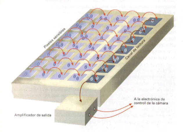
Figure 28 CCD device reading process ... 27
Figure 29 PLI functioning diagram ... 28
Figure 30 PLI Semilab ... 28
Figure 31 PLI inside ... 29
Figure 32 Mono as-cut wafer... 31
Figure 33 positions ... 32
Figure 34 broken sample ... 32
Figure 35 mono cell ... 33
Figure 36 Three recombination mechanism ... 35
xiv
Figure 38 μ-PCD diagram and signal response ... 37
Figure 39 MDP Freiberg Inside ... 37
Figure 40 EM devices MDP ... 38
Figure 41 Quasi-steady-state signal of photoconductivity ... 39
Figure 42 Minimum pulse for QSS signal ... 39
Figure 43 Efficiency vs Lifetime ... 41
Figure 44 IV tester diagram ... 42
Figure 45 Lamp main components ... 43
Figure 46 Solar Cell platform ... 43
Figure 47 IV curve ... 45
Figure 48 internal scratch PLI ... 47
Figure 49 PLI repeated measurement same position ... 48
Figure 50 Positions scheme ... 48
Figure 51 PLI different positions... 49
Figure 52 Broken cell ... 50
Figure 53 PLI multi and mono cell ... 50
Figure 54 stable signal ... 51
Figure 55 lifetime colours scale ... 51
Figure 56 Lifetime representation ... 52
Figure 57 statistics data ... 52
Figure 58 lifetime histogram ... 52
Figure 59 IV Result ... 53
Figure 60 Irradiance and Temperature IV test... 54
Figure 61 IV results ... 54
Figure 62 PLI data all positions ... 56
Figure 63 PLI data separated positions with colours ... 57
Figure 64 MDP Histogram ... 58
Figure 65 Histogram comparison PLI & MDP ... 60
Figure 66 Deviation tendency ... 61
Figure 67 Histogram ... 61
Figure 68 Lifetime vs efficiency tendency ... 62
Figure 69 tight interval in normal distribution ... 63
xv
List of tables
Table 1 PLI parameters... 30
Table 2 several cells ... 34
Table 3 MDP Laser ... 38
Table 4 MDP microwaves ... 38
Table 5 I-V tester parameters ... 44
Table 6 Solar cells ... 44
Table 7 IV efficiency data ... 54
Table 8 Summary for ANOVA analysis... 55
Table 9 ANOVA analysis ... 56
Table 10 Summary for ANOVA analysis... 58
Table 11 ANOVA analysis ... 58
Table 12 Summary for ANOVA analysis... 59
Table 13 ANOVA analysis ... 59
Table 14 Data results ... 62
Table 15 Lifetime data for the PLI ... 68
Table 16 Lifetime averages of the wafers in the PLI ... 69
Table 17 MDP lifetime data ... 70
xvi
Notation and Keywords
ANOVA: Analysis of Variance IV:
Intensity-Voltage testing
Lifetime: minority carrier lifetime
MDP: Microwave Detected Photoconductivity
μ-PCD: Micro Photo-Conductivity Decay
PLI: Photo-Luminescence Inline
QSS: Queasy-Steady-State
Planck constant: ℎ = 6.63 𝑥 10−34[J s]
Speed of light in vacuum: 𝐶 = 299792458 𝑚/𝑠
Excess carrier concentration: n
Minority carrier lifetime: τ
1
2
Chapter 1: Electromagnetic radiation of the light
Wave-particle duality
Most of the properties of the electromagnetic radiation are explained with the sinusoidal model. Unlike other sine waves, light does not need any medium for the transmission through the space. But when we try to explain phenomena like the energy absorption or emission the classic wave model starts failing. Hence we attend to the wave-particle duality which uses the sinusoidal wave and the properties of the particles, two models that complement each other.
To understand this process we contemplate the light as a particle flow called photons. This theory explains the radiation and emission of the energy flow but the corpuscular theory of light cannot explain phenomena like reflection, refraction, interferences… Compared to classical wave model, the energy of the photon is related with the frequency of the wave.
[1]
Wave model
Perpendicular to the propagation direction of the light there are associated magnetic fields in phase with electric fields also at right angle to each other.
3
In the Figure 2 all the oscillations are polarized in the same plane. To explain the wave parameters we just take into account the electric component avoiding the magnetic field.
Figure 2 Electric component of the EM wave
Amplitude (A): size of the largest vector in the maximum point of the wave. [m]
Period (p): time between two consecutive maximums (or minimums). [s]
Frequency (ν): number of oscillations in one second. [Hz]
Wavelength (λ): distance between two equivalent points, like maximums. [m]
Velocity of propagation: Vi = ν λ [m/s]
Intensity: 𝐼 = 𝑃
𝑆 (𝑠𝑢𝑟𝑓𝑎𝑐𝑒) [W/m
2]
Energy: 𝐸 = ℎ 𝑣 = ℎ𝑐
λ [J]
Planck constant: ℎ = 6.63 𝑥 10−34[J s]
Speed of light in vacuum: 𝐶 = 299792458 𝑚/𝑠
Power: 𝑃 = 𝐸/𝑡 [W]
Frequency depends on the emission source, velocity and wavelength depend on the propagation medium.
4
The electromagnetic spectrum
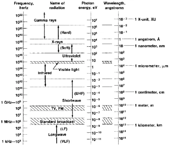
Depending on the parameters of the wave we have all the electromagnetic spectrum which allows us to characterize the different types of radiation usually classified according to their frequency or wavelength. In Figures 3 and 4 we can see the different zones of the spectrum catalogued in function of their practical applications.
[1]
Figure 3 Visible spectrum compared to the whole spectrum
5
Lambert-Beer law
Each semiconductor has his own absorption spectrum, being the absorbance (A) the relation between the power of the radiation that goes through the sample (P) and the receiving radiation (P0), as showed in the attached figure.
Figure 5 Absorbance through any material
𝐴 = − log 𝑃/𝑃0
Eq 1
The higher the absorbance coefficient (A), the more thin can the wafer in question, because the wave will need to advance less distance to be completely absorbed by the material. The absorbance is a function of the wavelength so for determined wavelengths it will be impossible to absorb the receiving radiation. In Figure 6 we show the absorbance coefficient for each wavelenght in silicon.
6
Energy states-quantum theory
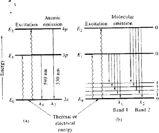
The theory introduced by Max Planck is based on two main points. The first one is that the atoms, ions and molecules can only exist for determined and discrete values of energy, and when they change the state they absorb the amount of energy defined by the difference between the two different states. The second principle of the theory is used to explain the relation between the amounts of energy absorbed or emitted by the atoms changing state and the wavelength of the radiation. This principle was also described by Niels Bohr to describe his postulates afterwards.
Figure 7 Absorption and emission
𝐸1 − 𝐸0 = ℎ 𝑥 𝑣 = ℎ𝑐 𝜆
Eq 2
Being E0 the ground-state and E1 the excited energy level. h is the Planck constant and v the frequency characteristic of the electromagnetic wave emitted. The different energy states are known as electronic states. In parallel, in the molecules, inside of each electronic state there are vibrational states defining the vibration between the particles. In the same way, defining the parameter of the rotation there are also rotational states. The energy associated to the band of the molecule is made up three different components.
[2]
𝐸 = 𝐸 𝑒𝑙𝑒𝑐𝑡𝑟𝑜𝑛𝑖𝑐 + 𝐸 𝑣𝑖𝑏𝑟𝑎𝑡𝑖𝑜𝑛𝑎𝑙 + 𝐸 𝑟𝑜𝑡𝑎𝑡𝑖𝑜𝑛𝑎𝑙
Eq 3
7
Figure 8 Electrons jumping between the different energy levels
When an electron returns from an excited level to the ground-state the electromagnetic radiation is originated in a specific characteristic frequency. In the Figure 8 (a) we see the different electronic levels, and in the Figure 8 (b) we see in the ground state level, the vibrational levels superimposed to the ground state one. The vibrational levels for the excited states have been omitted because the lifetime of those is too short compared with the excited level one, so that the relaxation of the electron to the lower levels is normally from the lowest vibrational level of the excited energy state. The diagram is not completely representative because the number of the lines should be higher since to all the vibrational states you have to add all the rotational states for a real molecule.
[1]
8
Chapter 2: Silicon as semiconductor
Photovoltaic effect
The photovoltaic effect is based on the property of semiconductor materials, which are able to increase the density of free electrons under external stimuli like radiation. The energy received from the striking photons is absorbed by the valence electrons exciting them in to free electrons, able to move within the material.
In the branch of electrical properties there are three types of materials: conductors, insulators and semiconductors. Conductors are materials, mainly metals, with many free electrons able to carry electrical current, which gives them a conductivity of around 106 mho/cm. Insulator materials, are basically the opposite, there are no free electrons able to move, their conductivity is about 10-11 mho/cm. Between them, we find semiconductors; Their conductivity can be modified to have a conductivity of 0.001 mho/cm to 1000 mho/cm.
[2] [3] [4]
Electron configuration and lattice structure
Silicon has the following electronic configuration, 1s2 2s2 2p6 3s2 3p2, which means that there are four free electrons in the last energetic level (Figure 9), each silicon atom shares these four electrons to form the crystalline structure using covalent bonds. Each atom is located in the centre of a figured tetrahedron, and the corners occupied by other similar atoms.
9
Figure 10 Silicon bonds tetrahedron
This Figure 10 corresponds to the image of the unit cell, which will be repeated in the three dimensions of the space to form the diamond lattice structure (Figure 11). It can also form the zinc-blende crystal structure in combination with elements from columns III and V of the periodic table.
Figure 11 Silicon lattice
Closest electrons to the nucleus do not participate in the physical phenomena due to the high electrostatic attraction. However the covalent bonds and the electric current are caused by the electrons in the last occupied band with the highest levels of energy for the ground-state atoms.
10
Energy band theory
The behaviour of the electrical properties in the semiconductors can be explained with the energy band theory.
Each band corresponds to an energy level, which could be infinite. The lowest level corresponds to the core electrons strongly bound to the atoms. The last band which contains non-excited electrons, is called the valence band, as temperature of the atom increases the electrons start ``jumping´´ into the higher energy level.
The next band, above the valence one is known as conduction band. It is where the excited electrons are free to move. The lowest energy of the conduction band minus the highest of the valence band is the "forbidden gap" or "bandgap".
[6]
Figure 12 Energy gaps
In the Figure 12 we can see the difference between an insulator (A) a metal (B) and a semiconductor (C). Following this energy band theory the difference between an insulator and a semiconductor resides in the size of the forbidden gap Eg.
Increasing the temperature from 0 K, the kinetic energy of each atom in the lattice increases (collision theory) and also the energy of the correspondent electrons increases. Some of them will then achieve enough energy to reach the conduction band, where they are allowed to take part in the current flow. Therefore at 0 K the conduction band of the semiconductors is empty of electrons.
11 electrons in the conduction band, has to be the same as the amount of holes in the valence band, to preserve the total charge of the molecule.
[2]
Intrinsic semiconductors are not really useful either as conductors or as insulators so that we can modify their electrical properties by adding some impurities. The process to combine a semiconductor with some other atoms in a controlled way with a determined purpose is called doping.
As we already know, silicon (and some other semiconductors) have 4 electrons in the valence band, so atoms which belong to the previous and next groups in the periodic table (groups 3 and 5) are used.
Extrinsic semiconductors
The elements in group V of the periodic table have 5 electrons in the valence band, hence, when inserted in the silicon lattice there will be an extra electron with free movement in the crystalline structure acting like a charge carrier. This groups of elements, able to give an electron to the crystal lattice are known as donors, like Arsenic (As) or Phosphorous (P). This results in an N (negative) type semiconductor, where the majority carriers are the electrons, in a higher concentration than the positive carriers, the holes.
12
Figure 13 Impurities in silicon lattice, (a) donor, (b) acceptor
Figure 14 zinc-blende structure
Changing some of the components of the crystal also changes the structure, modifying the diamond lattice structure into zinc-blende crystal structure (Figure 14).
13
Chapter 3: The solar cell
Photons Energy
Photovoltaic systems use a semiconductor compound to transform radiation into electricity. The photovoltaic solar cell is an electronic device able to convert solar radiation into electric energy. The energy of the solar radiation is absorbed by the cell as photons, able to excite the electrons generating the current carriers, the hole-electron pair. Electric current results from the positively charged holes and negatively charged electrons generated by the incoming light into the doped semiconductor. We could separate the electrons and the holes by applying an electric field with a battery but that would be nonsense if the point of the device is to generate electricity. So we need to generate an electric field without an external electric source to separate the charge carriers producing potential difference across the semiconductor known as photo-voltage. That voltage generates a photocurrent which represents a net flow of energy.
[7] [2]
PN Junction
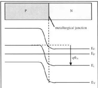
A PN junction is created to generate an electric field in the semiconductor without needing an external load. The PN junction is made by connecting together two different type of semiconductors, one doped with donors and the other one doped with acceptors, in other words, an N-type with a P-type, which can be made of the same semiconductors in the case of a homojunction or two different semiconductors in the case of heterojunction. The surface where they are connected is known as the ``metallurgical junction´´. The electric effect originated in the depletion zone of the PN junction is essential in the solar cells mechanism, once the electrical voltage is generated, the electron travels to the positive charge in the P-type material through the external circuit creating a flow of electric current.
14
Figure 15 PN junction
Figure 16 PN junction energy bands
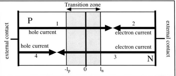
Electrons diffuse from the N-type region into the P-type one leaving behind them the correspondent ionized atom, not able to move within the crystal lattice. This region positively charged into the N-type semiconductor is depleted of electrons. It also happens on the other side where we can find a region depleted of holes, negatively charged in the p-type region. These two regions, together, are known as depletion region or transition region where the magnitude of the current is really small because anly minority carriers are involved.
15
Figure 17 PN electrons diagram
Solar Cell
Figure 18 Solar Cell scheme
16
wavelengths coincident with the ones necessary to excite the electrons in the valence band. Some cells also have some furrows and other textures created for the same purpose.
[8] [9]
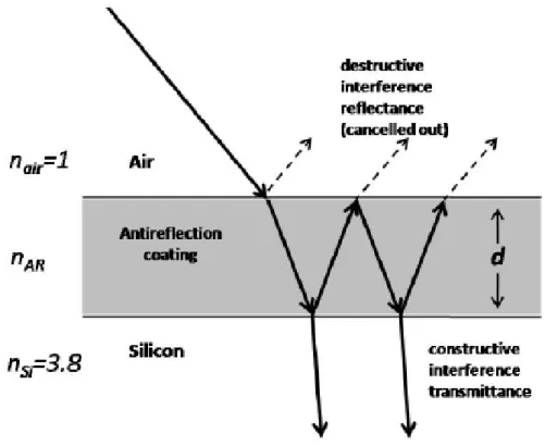
Figure 19 AR layer
Then we find the metallized grid made of thin fingers, with a critical design. It must guarantee the correct collection of the electrons within the device with the minimum electrical resistance. It also must allow the solar light to arrive to the semiconductor with the minimum shadow. Gathering all the contacts of the metallized grid we find the bus bars. Each sample can be designed with different amounts of them in order to facilitate the electrical contact.
Below that is the specific material which gives to the cell its specific properties, the PN junction. The cells we used during this project were made of homo-junction of silicon. The properties of the material in the junction are vital to the correct working of the solar cell.
Finally the back contact to close the circuit and give the structure rigidity and balance. We have just explained the basic model of the solar cell. Based on that we can find many more variations in all the parts of the design.
17
Mono/Multi Crystalline Wafer
There are several types of solar cells, especially when we focus on the structure of the semiconductor. Typically silicon has been used as a one single crystal, where the atoms are perfectly ordered in the lattice in a predictable and uniform way. To produce that in the industry they need to use a very specific and exigent process which is very expensive especially in terms of energy. The heating speed must be low and the product is an ingot in cylindrical shape. In contrast we find the amorphous silicon, completely characterized by the lack of order in the structure. And in the middle, between them, we can talk about the polycrystalline, manufactured with a faster and easier industrial process than monocrystalline. The process is energetically cheaper. It gives origin to more than one nucleation centre, whereby the crystalline lattices start growing up forming several of them in each sample. This kind of silicon ingots are characterized by the grain boundaries, where we can see clearly the separation between the different crystals.
[2]
The grain boundaries have an important effect on the properties. Polycrystalline cells have a bit lower efficiency due to these boundaries between crystals but also they have a better behaviour under hot temperatures. So we have to decide between mono and multi cells bearing in mind many different factors such as the weather, the geography or different aspects deeply explained in many several studies.
18
Figure 21 Mono-crystalline wafer and Multi-crystalline wafer
The manufacturing process of multi-crystalline silicon is simpler and requires less costs of energy and money. That is because the manufacturing of the single crystals requires a harder process with more stages and better controls to avoid the generation of several nucleation centres.
Also mono wafers are more compatible with the thin films than the multi ones. Both types of cells, under the same conditions have the same lifespan.
19
Chapter 4: Lifetime and recombination
Previously we have explained the importance of the generation of the pair electron-hole carriers, and we are about to explain the influence of the time between the generation of the carrier and its dissipation or recombination.
The time to recombine the minority carrier is called Lifetime and has big consequences on the quality of the silicon wafers. In the P-type wafers the minority carrier is the electron, in contrast with N-type, where the lifetime refers to the recombination of the holes.
The cell’s output current is related with the recombination lifetime because it takes some time for the electron traveling across the wafer to the PN junction so that is only possible if the lifetime of the minority carrier is enough.
[11]
Elevated values of the lifetime are indicators of good quality of the silicon wafers but the lifetime is hard to measure, especially in the industry, where a low value of the lifetime can be a symptom of an error in the process, degradation or deterioration of the material or even impurities which can affect the performance.
[12]
It is especially important measuring the minority carrier lifetime, especially in the finished solar cell to determine the quality of the industrial processing due to any change in this parameter would suggest problems in the diffusion processing or during the thermal annealing.
[13]
There are several studies about measuring the lifetime. Scientific papers support many different methods and techniques to quantify the lifetime, but there are basically two approaches, the steady-state and the decay method. In both of them we need to know the
concentration in excess of electrons (Δn). n would be electrons for p-type material or, for a general case, n will be the minority carrier.
The first approach is based on the maintenance of a constant steady-state generation of
electrons. Being in a steady-state process the generation (Gl) matches their recombination(Δn/t). (QSS-PC technique)
𝐺𝑙 =Δn 𝑡
20
The second one is the abrupt termination of the generation of electrons, so that the photo-generation is zero and the recombination is the only reason for changes in the excess concentration of electrons. (μ-PCD technique)
𝑑𝑛 𝑑𝑡 = −
Δn 𝑡
Eq 5
* Now there is no steady-state, the generation is zero, so it is no longer equal to the recombination.
*notice the minus sign in the equation which shows that is the minority carrier the one which is recombining.
[11]
There are several methods to measure the lifetime based on many different physical properties, Figure 22.
21
Chapter 5: Photoluminescence as a physical Phenomenon
The luminescence is a physical Phenomenon originated by the absorption of the energy by the electrons and their subsequent emission. When an atom is excited there are different mechanism by means of which the electrons lose the extra energy.
Figure 23 Energy absorption (a), thermal relaxation (b) and radioactive relaxation (c)
Non radiative relaxation.
As we see in Figure 23 (b), in the non-radiative relaxation, the electrons lose the energy through little steps in which the exciting energy turns into kinetic energy in the adjacent particles. That has thermal consequences in the system increasing the temperature.
22
Luminescence
There are also radiative mechanisms for which the excited electrons go back to the ground state. When the relaxing of the electron produces radiation, it is called luminescence. If it radiates because previously receiving an electromagnetic wave proceeding from the light, this phenomenon is called photoluminescence.
The phosphorescence is a slow mechanism, in which emission of the radiation can take even a few minutes with continuous emission until the finalization of the absorbance of the radiation. However the fluorescence is a faster process where the emission of the radiation ends about 10-5 s after the finalization of the receiving radiation.
Resonance fluorescence happens when the receiving energy is exactly the same as the difference between the excited state and the ground state so that the emission afterwards is exactly equal to the receiving emission. As we see in Figure 24 the energy of the
received and emitted radiation is 𝐸 = 𝐸𝑖 − 𝐸0 where i is one of the excited states.
Figure 24 Fluorescence
When the vibrational levels of the different energy states come into play, the change in emitted energy, the lifetime of the vibrational level is smaller than the excited one, so that the thermal losses (due to vibrational levels) will be previous than electronic relaxation. So that the radiation emitted will be smaller than the absorbed one (due to the thermal losses), decreasing the frequency. Therefore the frequency of the electromagnetic wave emitted in the luminescence will be lower, so that, the wavelength will be higher than that absorbed. The non-resonance fluorescence is a result of the numerous vibrational states.
23
Figure 25 Absorption vs fluorescence Wavelength
When an energy wave is absorbed and emitted afterwards it suffers a loss of energy through the process which means a change in the wavelength. Following the Planck Equation the loss of energy involves a loss in the EM frequency and a gain in the EM wavelength.
𝐸 = ℎ 𝑥 𝑣 =ℎ𝑐 λ
Eq 6
The sample material must have been radiated with a monochromatic beam in a specific wavelength. And in response, will be emitted with the same intensity but with lower frequency.
[14]
24
25
Chapter 6: Photoluminescence as a technique
Justification of the experiment
As we have explained, there are some parameters related to the lattice and the distribution of the electrons in the atoms which have a direct influence on the properties of the semiconductors used to manufacture the solar cells. Being able to know these properties allow us to know if the samples have been manufactured successfully. But it is not useful just for checking the completed solar cells. One of the best points of the Photoluminescence tool is the possibility of measuring the samples in any moment of the process, since they are still as-cut wafers till we have the finalized cells.
The capacity to measure them at any time of the process is not the only characteristic of the PL. The PL measurement is really fast, it just takes a few seconds to irradiate the sample and collect the result, as an image of the wafer in analysis. It is a really high resolution and versatile technique, useful in the entire photovoltaic value chain.
[15] [16]
Usually the tool is used to analyse the defects in multi-crystalline wafers such a dislocations, interstitial defects or grain boundaries. Current assessments have shown that the electric parameters of a solar cell can be predicted by PL measurements. High efficiency solar cells, manufactured from Czochralski silicon, suffer a loss in their efficiency due to a defect which appears as dark rings in PL imaging. Also analysing bricks of silicon before the wafer manufacture.
[17] [18]
Nevertheless our purpose is quite different, we are not trying to know the defects in the structure of the cell, instead we want to use the PL to know the quality of the wafer, in terms of finding any internal or surface defect which can affect the performance or correlating the results read in the PL to approximate the lifetime of the silicon, which as we know, has direct influence with the current generated and the performance of the cells.
Doing the experiments with mono-wafers allowed us to expect repeatable results. Without having any one of the defects of the multi-wafers the results will be more repeatable and stable. The result received will be interpreted through a mathematical correlation to approximate the lifetime. Numeric data results which will be useful to know the quality of the sample analysed.
26
During the test, we must avoid the presence of the solar light (or any kind of light) that can interference with the radiation emitted from the wafer, ruining the results.
We are describing the methodology of the experiment and the treatment of the data in order to obtain consistent results which highlight the usefulness of the photoluminescence technique to analyse the wafers/cells.
Specific equipment
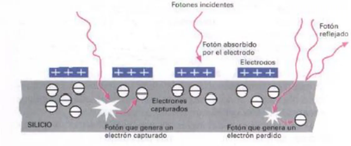
The sample is placed on a conveyor belt able to control the entrance and the way out of the sample into the machine. Once inside the machine, a laser beam is activated with a determined frequency and intensity to be absorbed by the silicon with enough energy to overcome the bandgap. The precision in the receiving laser is fundamental, due to those electrons out of the absorption spectrum of the specific material will pass through the sample without the wanted effect. The selected laser has a maximum power of 45 W and a wavelength of 915 nm.
Once the radiation is absorbed, the emitted radiation has also to be interpreted by a specific camera, and the infrared camera used to read the emitted radiation is the CCD camera (Charge-couple device). The CCD cameras are based on the photoelectric effect. To manufacture them a semiconductor like Silicon or InGaAs is used. One of the faces of the semiconductor is covered by small electrodes positively charged which will accumulate the electrons generated in the semiconductor by the light.
[10]
27
Figure 28 CCD device reading process
The radiation emitted read by the camera is dependent on the recombination of the excited electrons. The intensity of the radiation is inversely proportional to the impurity concentrations and defect density.
Once we start the measurement the conveyor belt starts moving the sample. The wafer/cell enters into the dark box (the light of the environment might produce interferences). The laser source starts emitting the laser beam. It is reflected in a mirror and refracted into a cylindrical lens. Once the light is absorbed by the silicon, the luminescence response is recorded by the infrared camera.
During all this process the conveyor belt moves causing a continuous movement of the sample, which will be stopped once it arrives at a stopping sensor.
28
Figure 29 PLI functioning diagram
29
Figure 31 PLI inside
30
Experimentation
First of all we had to adjust the parameters of the machine to run the required experiment. It should be noted that the parameter shall change for each kind of sample to measure. We have run the PLI with some different groups of samples.
RECIPE Cell Mono 125 As-cut mono 125
Analysys
BadFingerLimit 0.2 0.2
ChamferLimit_us 0.5 0.5
DarkEdgeAreaMax_percent 5 5
DarkEdgeLimit_us 1 1
DarkLimit 1 1
DefectAreaLimit 0,26 0,25
DefectIntensityTreshold -1 -1
DefectTreshold 1 1
EdgeGrainDefectLimit 0.08 0.08
GlobalTreshold 1.2 0.7
GrainDefectLimit 0.2 0.1
MaximumEfficiency 16.8 16.8
SeparateGrainDefects Y Y
Image correction
Dark 104us_45W 103us_45W
Flat 104us_45W 103us_45W
Misc
Belt Speed [mm/s] 150 150
Classifier default default
DefectFeatureExtraction Y Y
FilterMonoWafer N N
OnlineLifetimeCalibration Y Y
Settings
BiasLampPower 0 0
ExposisionTime_us 1040 1030
FilterType BandToBand BandToBand
LaserPower_W 5 45
LineCount 1200 1200
UpcdRecipe multicell.rcp multiascut.rcp
Wafer
NumberOfBusBars 2 0
ProcessStep Cell Ascut
Wafer fill factor [%] 50 21.2
WaferSize 125 125
WaferType Mono SquareMono
31 First measurement
The first samples consisted of 40 as-cut wafers of monocrystalline silicon P-type/Boron, square 125 x 125 mm2 and 250 µm thick.
Figure 32 Mono as-cut wafer
The purpose of the first set of wafers was to analyse the consistency of the PL depending on the side or on the position of the wafer we are measuring and the repeatability of those results. To that end we have analysed the 40 samples in four different positions, three different times each position.
Position 1: Basis position. Position 2: turn 90º position 1.
32
Figure 33 positions
The wafers were not marked in any point, so it should be pointed out the necessity of a methodology which allows keeping all the samples in the required position without losing the reference. It is also highly required that the samples are treated carefully; the crystalline structure is really fragile, especially when we are working with samples around 240 μm thick. Despite all the care, we could not avoid breaking some of the samples.
33 Second measurement
Once the consistency and the repeatability of the tool was established we wanted to focus now on the application of the result and the comparison with the quality of the samples. The samples were mono-crystalline solar cells, pseudo square (due to the chamfer corner) 125 x 125 mm2 and they also have their surface passivated. The area of the cell was approximated to 155 cm2. We have measured a pack of 10 solar cells, just one time each.
Figure 35 mono cell
34 Third measurement
In this case, in order to contrast with the previous one, different cells have been selected randomly, with different characteristics, sizes and supposedly different values of lifetime. In this case the parameters of the recipe of the PLI tool have been improved for each type of cell, to allow the software of the machine doing the correct reading.
SAMPLE TYPE BUS
BARS
SIDE (mm) CORNER AREA (cm2)
A Multi 2 156 Right angle 243.4
B Mono 3 156 Chamfer 239
C Mono 3 156 Chamfer 239
D Mono 3 156 Chamfer 239
E Mono 2 125 Chamfer 155
F Mono 2 125 Chamfer 155
Table 2 several cells
35
Chapter 7: Microwave detected photoconductivity (MDP)
Justification of the experiment
The purpose of this experiment was the analysis of the lifetime of the as-cut wafers. The minority carrier lifetime is one of most important parameters related to the wafer and their future behaviour as PV Cells. The lifetime depends of the bulk of the semiconductor and the surface properties.
The minority carrier lifetime measured in this experiment is the effective one, if we want to know the bulk lifetime, the program suggest us an option, based in the diffusion coefficient Dn, and the wafer thickness.
1 recombine. The minority carrier lifetime depends also on the number and type of defects and the injection level (excess carrier concentration).
[19] [5]
36
Auger recombination happens when there is a high level of excess of carrier concentration, so that when the molecule is highly doped and the injection level is quite important. Schockley-Read-Hall takes place in semiconductors with an indirect bandgap like Silicon and Radiative when they have a direct bandgap like the case of the GaAs. Different electron recombination phenomena explained in the scheme of the Figure 36.
1 conductivity produced by the excess of minority carriers will be increased. As we have said, there is no direct contact with the sample, so the test involves the reflection of the microwaves, which will be affected by the conductivity of the wafer. A radiation in the microwave wavelength is originated and replicated in a cavity, a sensor receive back the microwave signal reflected, which will be modified in function of the conductivity of the sample. To modify the conductivity of the sample we use an infrared laser which will originate the excitation of the electrons generating the excess of carriers in the sample. We use the laser with a strong enough pulse to originate a quasi-steady-state (QSS), when the excitation of electrons is equal to the recombination so the injection remains constant. Once the steady-state is reached, we stop the laser radiation, observing the changes in the microwaves received caused by the changes in the photoconductivity.
37
The photoconductivity is found by reading the microwave absorption during and after the electron excitation with a rectangular laser pulse. The microwave spectrometers used works with a frequency around 10 GHz which is bounced through a resonant cavity, being the sample electrically part of it therefore the physical properties are obtained in relation to the dielectric constant.
Figure 38 μ-PCD diagram and signal response
38
In the Figure 39 we can see the inside of the tool composed of the platform to place the sample to measure. The mechanism which allows the laser to move finding each point of the sample and the EM devices.
EM Device Power Class Wavelength
Laser 1000 mW 4 978 nm
Table 3 MDP Laser
EM Device Frequency [GHz] Power
Microwaves x-band, 9-10 Max 500 mW
Table 4 MDP microwaves
Figure 40 EM devices MDP
The MDP machine measures the lifetime pixel by pixel until completing the whole square of the wafer.
39
Figure 41 Quasi-steady-state signal of photoconductivity
Following the numbers of the Figure 41:
1. Generation of free careers 2. Traps filled with carriers 3. Recombination processes
5. Temporally shifted recombination of reemitted carriers
Experimental procedure
To make sure we are able to provoke in the sample a quasi-steady-state we need to try with different laser pulses, and attaching the response. We need a constant signal of photoconductivity. The proper software of the machine provides us a method to find the minimum pulse to work in a QSS mode, as shown in Figure 42.
40
As shown in Figure 42, the minimum pulse found for QSS was 12 µs, but we can observe that the signal on the top is not completely stabilized, and could change with each sample. For all that we set a pulse duration of 50 µs in order to make sure we are working in a quasi-steady state.
We also set the Laser in 50 Mw with a wavelength of 960 nm (infra-red spectrum). The step size of the sample will be 1 mm.
41
Chapter 8: I-V measurement system
Justification of the experiment
We have analysed different wafers by several methods in order to find out the quality of the as-cut wafers, but we also need a method to correlate the measured complete solar cells with their efficiency. In order to do that we have used the I-V measurement system.
Theoretically the higher the lifetime, the more time the electrons will be working in the conduction band once excited. We already know that the presence of these electrons in the conduction band in the PN junction is what generates the voltage which makes the current flow. So that we can assume that the higher lifetime the more energetically efficient the cell should be.
Figure 43 Efficiency (%) vs Lifetime (µs) [21]
As shown in the Figure 43, the efficiency has an asymptotic behaviour in relation with the bulk lifetime. We will test the efficiency of the solar cells measured in the PLI machine. We want to find a correlation between the minority carrier lifetime correlated in the PLI and the efficiency. To do that we will irradiate the solar cells imitating the sunlight and reading the current produced by the cell. Depending on the lifetime
measured in the PLI we can expect a dependency with the efficiency tested, as shown in the Figure 43.
42
Specific equipment
The system is composed of a light source which will be used for illuminating the samples. The wafer is connected to the load with several contacts. Voltage and current can be measured separately in order to avoid resistance errors.
Figure 44 IV tester diagram
Following the manual of the integrated cell tester:
``The SS150AAA-EM Solar Simulator is a system for generating light that matches the sun’s spectrum. The system provides controls for adjusting xenon lamp intensity, and manual/automatic shutter control.
Lamp used in this system is extremely stable and specially made for Solar Simulators. The NOMINAL LIFE of the lamp is 1,500 hours, where NOMINAL LIFE is defined as the time when the lamp intensity is expected to drop to 70% of the initial intensity.
Air Mass Filter - The Air Mass Filter is used to shape the spectrum of the Xenon lamp to match the sun’s spectra as closely as possible. Shutter Mechanism - The shutter mechanism is mounted on a rotary solenoid. Integrator Lens - Integrator lens for uniform dispersion of light intensity throughout the output beam. Collimating Lens - Lens for collimating the output light beam´´
43
Figure 45 Lamp main components
44
Light Source Steady State (Shutter Controlled)
Air Mass AM1.5G
Lamp lifetime 1,000 hours
Intensity Adjustment 100 mW/cm2 +/- 15%
Simulator class Class AAA
Spectral Match to ASTM E927 +/-25% or better
Temporal stability 2% or better
Non-uniformity of irradiance 2% or better
Dimensions (H x W x D), mm (in) 1,756 x 416 x 619 (69.1 x 16.4 x 24.4)
Voltage 220VAC Single Phase
Frequency 50-60 Hz
Max. Power 2,200 W
Weight 100 Kg (220 Lb)
Table 5 I-V tester parameters
Experimentation
The same cells studied in the PLI have been also measured in this experiment; pack of 10 solar cells mono-crystalline solar cells, pseudo square 125 x 125 mm2 and they also have the surface passivated. The area of the cell was approximated to 155 cm2. We have measured a pack of 10 solar cells, just one time each.
Like with the PLI, the samples measured belonged to the same lot, which implies similar values of lifetime. A tight interval can also provoke some errors in the statistics analysis which explains the third experiment.
In contrast, in the next set different cells with different characteristics, sizes and supposedly different values of lifetime were used.
45
The IV curve of the solar cells has the following parameters.
ISC: Short circuit current, higher value of the current obtained by the device as generator
when the voltage is zero.
VOC: Open circuit Voltage, maximun voltage from the solar cell when the current is zero.
VOC =nkt q ln (
𝐼𝑙 𝐼0+ 1)
Eq 10
n being the Ideality factor, T the temperature in Kelvin, Il the light generated current and I0 the dark saturation current.
Maximum power point: working point where the power produced by the cell is maximum.
𝑃𝑚 = 𝑉𝑚 ∗ 𝐼𝑚
The Fill Factor is the relation between the maximun power and the maximum Area in the graph set by Isc and Voc.
𝐹𝐹 = 𝑃𝑚 𝐼𝑠𝑐 ∗ 𝑉𝑜𝑐
Eq 11
And later we arrive to the wanted parameter, the efficiency, calculated as a function of the intensity of the light of the source and the intensity generated.
𝜂 =𝑃𝑚 𝑃𝑙
Eq 12
Figure 47 IV curve
46
47
Chapter 9: Results
PLI
As-cut wafers
The PLI, as previously introduced, gives us a flat image of each sample, and calculates the value of the lifetime.
First at all, we detect an thin fracture in one of the samples. It is important to point out that the fracture its not visible to the naked eye. This makes the sample really fragile, and we will notice that quickly. The sample broke while handling in the next measurements. For that reason, we can not take into account the lifetime data received for the sample, and it was removed for the following experiments.
Figure 48 internal scratch PLI
Internal scratches, dislocation defects and impurities around them are good points to the recombination of the electrons which reduces the lifetime of the minority carriers.
With the intent to analyze the repeatability of the tool, as explained in the previous chapters, each sample has been analyzed three different times in four different positions.
48
Figure 49 PLI repeated measurement same position
As we have already explained, the samples were also measured rotated and flipped to verify the role of the different positions in the results. To show the position in the machine, we have selected a sample with the corner broken, which facilitates the understanding of the different positions and the luminescence result. How the sample has been rotated and flipped was explained in chapter 6. If we focus on Figure 51 and we compare with the diagram of the relative positions (Figure 50) we realize that the rotation is inverse, that is because the image received of the sample is a reflection of the receiving laser, so the image is detected with the mirror effect, and also is the rotation and the flipped. When we introduce a sample in the machine, we receive the opposite image (like when we look in a mirror).
49
Figure 51 PLI different positions
As expected, we received a flat image, with no defects in the structure. We can clearly observe that this is a monocrystalline wafer due to the lack of grain boundaries. The machine also gives us a value of the lifetime, and the constant result allows us to characterize the machine with the measured lifetime. The table of the measured lifetime which accompany the luminescence image are shown in Appendix A.
Solar Cells
The solar cells were also measured with the PLI. In this case the metal connections and the bus bars of the cell hamper the collection of the luminescence response. Nevertheless the image received is clear enough to observe the existance of internal defects and to keep obtaining a flat image.
50
Figure 52 Broken cell
We show below in Figure 53 the difference between the luminescence produced in a mono-crystalline wafer and a multi one.
Figure 53 PLI multi and mono cell
51
MDP
First of all, we have to check that we obtained a correct response in the photoconductivity. If the signal received is unstable we must optimize the parameters of the transient and the pulse duration.
Figure 54 stable signal
In this case, the lifetime is measured pixel by pixel so we obtain a lifetime value for each point of the sample. Afterward the software created a representation of the wafer, generating a scale for the different values, and assigning each range of values different colours and generating with all that a pattern of the lifetime of the sample.
Figure 55 lifetime colours scale
52
Figure 56 Lifetime representation
The machine is also giving us a histogram which includes all the lifetime values of the sample. It also provides the basic statistics, average, median, standard deviation, minimum and maximum values.
Figure 57 statistics data
53
The evenness of both results of each sample is remarkable. The distribution of the results in the histogram, the statistical values and even the lifetime distribution in the representation of the sample are almost identical.
With the available data we have selected the average lifetime in order to compare them with the ones obtained in the PLI. In the following table we have the average lifetime of each sample.
The lifetime data are shown in Appendix C.
I-V testing
The cell is irradiated with external light. During this short period of time the external resistance changes from zero to infinite following Ohm’s law. This provides us from the intensity short circuit to the open circuit voltage. As a multiplication of the Intensity and the Voltage we find the Power, represented as blue in the graph below.
𝑉 = 𝑅 ∗ 𝐼
Eq 13
𝑃 = 𝑉 ∗ 𝐼
Eq 14
Figure 59 IV Result
54
Figure 60 Irradiance and Temperature IV test
55
Chapter 10: Data analysis and conclusions
PLI
Once the luminescence images have been analysed, we must interpret now all the data collected, four positions, 39 samples, three repetition that make a population of 468 values organized in twelve different columns, as shown in APPENDIX A.
We have used the statistics analysis known as analysis of variance, single factor with the Microsoft Excel. The independent variable is associated to the different measurements and the dependent one to the lifetime values. First of all we set the null hypothesis, the different population are statistically equal and the different times we run the PLI has no influence in the lifetime values. If we finally reject the null hypothesis accepting the alternative hypothesis of the difference in the different groups, we will need to use the TUKEY analysis to determine which column is different seeing if any specific position causes the variation.
We have plotted the histograms of the data checking if the data follow a normal distribution, necessary condition to use the ANOVA analysis. This analysis has been made several times with different parameters and it has shown very good results, allowing us to set a statistical significance (α) of 0.0001.
SUMMARY
56
The P-value is higher than the statistical significance (α) which means that we accept the null hypothesis, all the data population of table 7, those correspond with the PLI are statistically similar with a reliability of 99.99 %. The F factor is lower than the critical F which also means that the different columns, which correspond to the different runs realized, have no influence in the lifetime data.
All this statistical analysis allows us to say that the results of machine are absolutely repetitive and that the positions have no influence on the result. In the figure below we show the histogram for all the lifetime data obtained in the PLI for the as-cut wafers.
Figure 62 PLI data all positions
0
2,50 2,54 2,58 2,62 2,66 2,70 2,74 2,78 2,82 2,86 2,90 2,94 2,98 3,02 3,06 3,10 3,14 3,18 3,22 3,26 3,30 3,34 3,38 3,42 3,46 3,50
57
We calculate and plot now a histogram with the mean values of the PLI lifetime data but separated in their different positions, in black, position 1, in red, position 2, green, position 3, and blue, position 4. We can see what we have demonstrated in the statistical analysis; there are no significant differences in their distributions so we assume that it does not matter the position of the sample when we measure it in the PLI. We can see the average lifetime values for the different positions shown in Appendix B.
Figure 63 PLI data separated positions with colours
0
2,50 2,54 2,58 2,62 2,66 2,70 2,74 2,78 2,82 2,86 2,90 2,94 2,98 3,02 3,06 3,10 3,14 3,18 3,22 3,26 3,30 3,34 3,38 3,42 3,46 3,50
Fr
58
MDP
We have executed the same analysis with the data of the MDP. ANOVA single factor, In this case, the results of the two times we have run the samples are almost the same, so we expect even more consistent results. We use the same statistical significance (α=0.0001). The P-value is close to the unit and the F one is almost null. That clearly means we can accept the null hypothesis of the similarity of the results with 99.99 % of certainty. We show the data tables and analysis below. In the histogram we can note what the statistical ANALYSIS reveals, the distributions of the both measurements realized are quite the same. Data in Appendix C.
SUMMARY
Groups Count Sum (µs) Arith. Mean (µs) Variance
Column 1 39 124,07 3,18 0,037
Column 2 39 124,06 3,18 0,038
Table 10 Summary for ANOVA analysis
ANOVA
3,00 3,02 3,04 3,06 3,08 3,10 3,12 3,14 3,16 3,18 3,20 3,22 3,24 3,26 3,28 3,30 3,32 3,34 3,36 3,38 3,40 3,42 3,44 3,46 3,48 3,50
59
Comparison MDP/PLI
Once both tools have been analysed separately we need to compare them (PLI and MDP). We have already explained that the MDP is measuring the lifetime directly and the PLI is not; it is just a correlation computed.
First we create a table, with the mean data for each tool (that is possible because we have statistically proved the consistency of the data groups), then we realize the ANOVA one factor analysis like in the previous experiments. This time, the P-value is almost null, and of course, lower than the statistical significance (α=0.0001) which means we reject the null hypothesis and we confirm the alternative one, we can be 99.99 % confident that the population groups (MDP and PLI arithmetical means) are statistically different. The F factor is also really higher than the critical one, which reveals that the type of machine has direct influence on the result. To explain data we use the histogram to compare the distribution of the data. Data in Appendix D.
SUMMARY
Grupos Count Sum (µs) Arith. Mean (µs) Variance
Columna 1 39 110,1725 2,8249359 0,04711551
Columna 2 39 124,065 3,18115385 0,03774008
Table 12 Summary for ANOVA analysis
60
Figure 65 Histogram comparison PLI & MDP
We calculate the average difference which is 0.356 μs, adding it to each value of the PLI result and plotting the distribution with the MDP one. We realize that correcting the deviation in the data, both distributions are really closer now. The medium deviation is 11.20 % over the MDP arithmetical average. This gap in the results is probably due to a shift in the calibration, the tools belong to different companies which probably designed a different calibration of the devices. It is also explained by the physical phenomena, as explained in the theoretical chapters; the lifetime is a function of the bulk lifetime and the recombination in the surface. Higher sensitivity of the PLI to the surface condition might also affect the results.
1
Following this equation, bulk lifetimes over 10 μs and important surface effects will provoke a dominant effect on the surface lifetime into the effective one. That might also be the cause of a lower result in the PLI measurements.
[24]
This effect, if it exists, would be removed, or at least mitigated, in the final solar cells, where the surface has been passivated in order to overcome this surface recombination. Increasing the
61
lifetime in the surface, you reduce the dominance of the surface over the effective lifetime measured.
The lifetime is also a function of the receiving radiation wavelength (and therefore also the emitted one). Both machines work in the infrared spectrum but they use have different wavelengths which could also partly explain a different effective lifetime in the measurements.
[25]
Despite this quite important deviation, the tendency of the PLI results and their distribution is completely adjusted to the MDP one, which means, that the PLI can be perfectly used to measure the quality of the samples. A higher value of lifetime involves a higher efficiency.
Figure 66 Deviation tendency
2,50 2,70 2,90 3,10 3,30 3,50 3,70 3,90 4,10 4,30
De
3,00 3,02 3,04 3,06 3,08 3,10 3,12 3,14 3,16 3,18 3,20 3,22 3,24 3,26 3,28 3,30 3,32 3,34 3,36 3,38 3,40 3,42 3,44 3,46 3,48 3,50
62
Lifetime vs efficiency
All this provides a perfect scenario to adjust a correlation between the lifetime measured and the quality of a sample and therefore the efficiency of the corresponding photovoltaic silicon cell.
We represent the efficiency vs the lifetime measured in the PLI.
SAMPLE PL [LIFETIME µs] PV [EFFICIENCY]
Figure 68 Lifetime vs efficiency tendency
10,00%
3,00 3,50 4,00 4,50 5,00 5,50 6,00 6,50 7,00
63
We can see in the diagram shown in Figure 68, a clear relation between the lifetime measured and the efficiency, which means that the PLI can be used to measure the quality of a sample and try to predict the efficiency.
The shape of the graph illustrated is not like the asymptotic curve we have seen in the literature review. This is probably due to the low number of samples we have analysed. 16 samples is not a population big enough to characterize perfectly the relation between these two parameters. A low number of samples means that the range of lifetimes measured is not wide enough, so the statistical analysis is not as complete as it should. In the images below we show how a too tight interval can affect the shape of the graph.
Figure 69 tight interval in normal distribution
64
Chapter 11: Future work
In the future, the software correlation to obtain the lifetime data with the PLI must be improved. One of the causes for this deviation between these two tools can be the different sensitivity to the surface effects.
I suggest the study of this effect by using Double side polished samples. The roughness of the surface can reflect the receiving radiation into several directions. With the utilization of plain samples the received light is absorbed in a uniform way and the penetration of the radiation is deeper and more efficient and this may banish all doubts between the surface effect and its consequences on the results.

![Figure 22 Classification of experimental methods for measuring minority carrier lifetime of semiconductors [5]](https://thumb-us.123doks.com/thumbv2/123dok_es/3902862.663111/36.892.121.805.559.928/figure-classification-experimental-methods-measuring-minority-lifetime-semiconductors.webp)