Instituto Tecnológico de Costa Rica
Escuela de Ingeniería Electrónica
“Media Independent Interface (MII) implementation and data processing on
FPGA for Fast ETHERNET transmission over Plastic Optical Fiber”
Politecnico di Torino
Julio César Ramírez Molina
200109454
Abstract
This thesis focuses on the design and implementation of a Media Converter, which
allows Ethernet Communication through 250 meters of Plastic Optical Fiber (POF).
Three subsystems constitute this system.
First, a configurable MII Interface which provides Full Duplex Communication
through the Ethernet at different data rates (10Mpbs and 100Mbps). The User
defines the data rate according to the capabilities of his Modulator.
The second subsystem is the Transmission Module. This module receives
Ethernet data provided by the MII interface in order to encode it. Then it generates
a Reed Solomon verifying sequence used by the receiver to correct the frame
errors and to certificate the frame accuracy.
Finally, the third subsystem is a Testing Unit. It is used in the development and
debugging process of the prototype. This module emulates a real data
transmission using a Pseudo Random Bit sequence (PRBS).
Table of Contents
3.3 PHYSICS AND ELECTRONICS PRINCIPLES DESCRIPTION... 15
4 METHODOLOGICAL PROCEDURES ... 19
4.1 PROBLEM DEFINITION... 19
4.2 INVESTIGATION AND SOLUTION SYNTHESIS... 19
4.3 SOLUTION IMPLEMENTATION... 20
5 DESCRIPTION OF THE SELECTED SOLUTION... 22
5.1 HARDWARE DESCRIPTION... 22
5.1.1 Hardware General Description ... 22
5.1.2 MII Initialization System... 24
5.1.2.1 Second Level Diagram... 25
5.1.2.2 Third Level Diagram... 26
5.1.3 Transmission System ... 30
5.1.3.1 First Level Diagram... 30
5.1.3.2 Second Level Diagram... 31
5.1.4 Testing System of the Media Converter ... 40
5.1.4.1 Traffic Generation Unit TGU ... 40U 5.1.4.2 Data Compilation Unit DCU ... 41
5.1.4.3 Control Unit ... 44
5.1.4.4 Download Unit... 45
5.1.5 Reconstruction of the Preamble ... 47
5.2 SOFTWARE DESCRIPTION... 50
6 RESULTS ANALYSIS... 52
7 CONCLUSIONS AND RECOMMENDATIONS ... 59
ANNEX1PHOTOS OF THE CARDS AND DEVICES UTILIZED TO IMPLEMENT THE SYSTEM... 77
ANNEX2DP83848NATIONAL INSTRUMENTS CARD... 79
ANNEX3NALLATECH PCICOMMUNICATION CORE APPLICATION NOTE... 80
ANNEX4VIRTEX 4FAMILY OVEVIEW... 81
ANNEX5SECOND PART OF THE IEEE802.3PROTOCOL... 82
ANNEX6XILINX CORE ASYNCHRONOUS FIFO V6.1... 83
ANNEX7XILINX CORE REED SOLOMON ENCODER V5.0... 84
Table of Figures
Fig.1.1. Block Diagram of the Media Converter... 9
Fig.3.1. Block Diagram of the Ethernet Interface... 12
Fig.3.2. IEEE 802.3 standard relationship to the OSI/IEC for Open System Interconnection... 15
Fig.5.1. BMCR writing and reading Protocols... 17
Fig.5.1. General Diagram of the System ... 23
Fig.5.2. CRGU Block Diagram... 24
Fig.5.3. CRGU Second Level Diagram... 26
Fig.5.4. CRGU_MII Third Level Diagram... 27
Fig.5.5. InitPHY Third Level Diagram ... 28
Fig.5.6. ControlGEN State Machine ... 29
Fig.5.7. First Level Diagram of the transmission system... 30
Fig.5.8. BLOCK A block diagram... 32
Fig.5.9. BLOCK B block diagram... 34
Fig.5.10. BLOCK C block diagram... 36
Fig.5.11. BLOCK D block diagram... 38
Fig.5.12. System Second level diagram. ... 39
Fig.5.13. Traffic Generation Unit Diagram ... 41
Fig.5.14. DCU First Level Diagram... 41
Fig.5.15. DCU Second Level Diagram... 43
Fig.5.16. State Diagram of the Control Unit... 44
Fig.5.17. PCI Communication Core block Diagram... 45
Fig.5.18. State Diagram of the Control Unit... 48
Fig.5.19. Block Diagram of the Preamble Generator... 49
Fig.5.20. Flow Diagram implemented for the Software Application... 51
Fig.6.1. PING summary in the Command Prompt ... 53
Fig.6.2. PING summary in the Command Prompt ... 53
Fig.6.3. PING summary in the Command Prompt ... 54
Fig.6.4. FPGA Utilization ... 56
Fig.6.5. Timing Summary of the Media Converter... 57
Fig.A.1. Test 1 Configuration... 66
Fig.A.2. Test 2 Configuration... 67
Fig.A.3. Test 3 Configuration... 68
Fig.A.4. Test 4 Configuration... 69
Fig.A.5. Testing Setup with the POF as a LOOPBACK ... 70
List of Tables
Table 5.1. CRGU Pinout Configuration... 25
Table 5.2. Truth Table of the ROM ... 28
Table 5.3. System Pinout Configuration ... 31
Table 5.4. Block A Pinout Configuration ... 33
Table 5.5. Block B Pinout Configuration ... 35
Table 5.6. Block C Pinout Configuration... 37
Table 5.7. Block D Pinout Configuration... 38
Table 5.8. DCU Pinout Configuration ... 42
Table 5.9. Core Pinout Configuration ... 46
Table 6.1 Results obtained from TEST1 ... 52
Table 6.2 Results obtained from TEST2 ... 52
1 Introduction
1.1 Problem Definition and Solution's Relevance
The goal of the project was to design and implement a Media Converter prototype
fully compatible with the Ethernet standard and able to transmit at a data rate of
100Mbps over 250 meters of Plastic Optical Fiber (POF). It’s important to notice
that It was programmed in VHDL and loaded in an FPGA (Field Programmable
Gate Array).
The project was developed in the PhotonLab, which is an experimental facility
product of the cooperation and joint-venture of the Politecnico di Torino and
"Istituto Superiore Mario Boella" (a private non-profit research center), both
located in Turin, Italy.
This thesis is part of a big European project called "POF-ALL ("Paving the Optical
Future with Affordable Lightning-fast Links"), which is sponsored by the European
Research Sixth Framework Program (FP6), involving 11 partners and a total
budget close to 3 Million Euros. POF-ALL develops a low-cost solution based in
POF to increase the broadband access and to give advantage, independence, and
better competitiveness to the European continent in the low-cost network access
technologies.
1.2 Problem Definition
1.2.1 Generalities
The research group required a programmable Ethernet interface in order to give to
the Media Converter a Full Duplex link with configurable data rates (10Mbps and
100Mbps) and autonegotiation capabilities (enable/disable). Also required the
design and implementation of a hardware architecture to perform tests to the
equalization algorithms designed by them.
1.2.2 Synthesis
The media converter requires a programmable ETHERNET link and the hardware
architectures needed to test the equalization algorithms of the Media Converter.
1.3 Selected Solution
The design of the media converter involves the development of an optical link to
and from the POF, an electrical link to and from the UTP Cat5 cable and a signal
processing module in charge of the protocol conversion. Consequently, the system
was divided in three main blocks, which are shown in figure 1.1.
The first module on the left implements the MII interface. It was implemented with
an special purpose card of National Instruments[
1] that is configured from the
FPGA Board and that has all the circuitry and capabilities needed for the
establishment of the Full Duplex link with data rates of 10Mbps and 100Mbps.
The center module in the diagram corresponds to the FPGA board and contains
not only the necessary logic to configure the MII interface, but also the hardware
architecture that execute the media conversion and the system field tests.
Finally, the last module on the right corresponds to a POF daughterboard
designed and implemented by the PhotonLab researchers. It is an special card
that converts the electrical signals into optical signals.
1
The datasheet of the DP83848National Instruments Card is shown in the ANNEX 2
2 Goal and Objectives
2.1 Goal
•
Design and implementation of a media converter prototype able to establish
Fast Ethernet communication at 100Mbps over 250 meters of POF.
2.2 General Objective
•
Provide the electronic structures to the media converter in order to establish
Fast Ethernet communication.
2.3 Specific Objectives
•
Implement the MII standard with the possibility of selecting between data
rates of 10 Mbps and 100Mbps.
3 Theoretical
Background
3.1 System Description
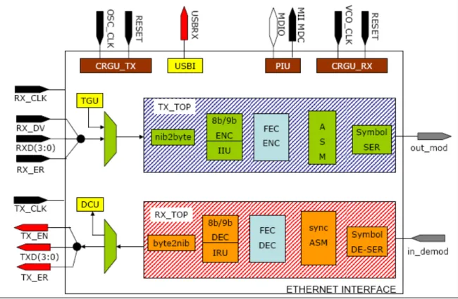
Figure 3.1 shows the block diagram of the system without the modulation and
demodulation blocks. The modules colored in green, brown and yellow are those
developed for this thesis, those in orange were implemented by other members of
the PhotonLab using the System Generator Tool of Matlab and finally the FEC
(Forward Error Correction), modules on sky blue corresponds to Xilinx Cores. Also
in this figure, the hierarchical configuration of the Transmission (highlighted in
blue) and Reception (highlighted in red) blocks can also be observed in this figure.
Fig.3.1. Block Diagram of the Ethernet Interface
The output pins of the system are colored in red whereas the inputs pins are black.
The gray pins on the right side of the diagram are the connections to the
modulation/demodulation blocks and finally the white pin on the top side of the
diagram is a bidirectional line connected to the National Instruments card.
At this point the operation of some blocks shown in the fig 3.1 will be detailed. The
brown modules are in charge of the DP83848 National Instruments Card
configuration (Physical Initialization Unit, PIU) and generation of the internal clocks
and resets(Clocks and Resets Generation Units, CRGU).
The green modules inside the Transmitter encode the information received in
order to facilitate the data recovery process on the receiver side. The data stream
is treated as follows: it’s received as nibbles (4 bit words) by the first module
(nib2byte) that concatenates two nibbles to form a byte word. Then the second
module (8b/9b) encodes each byte as a 9 bit word, preparing it for the FEC
module , where the data is encoded using the Reed Solomon Algorithm[3]. Once
the data is encoded, the ASM (Attached Synchronizing Mark) is inserted for
synchronization purposes and finally each 9 bit word is divided in 3 bit wide
symbols (Symbol SER) and sent to the modulator.
3.2 Existing Literature
The development of the project implied the study of the IEEE 802.3 standard in
order to understand the operation of the ETHERNET protocol. Also a Xilinx
Implementation Manual and a Nallatech Manual[6] were consulted. The first one
includes information regarding the synchronizing and processing of data, also the
operation of some Core Modules such as the DCMs for clock generation (Digital
Clock Manager[
1], the Asynchronous FIFOs as interfacing blocks between clock
domains[
2] and the Reed Solomon encoder/decoder used to guarantee the data
integrity. The second manual explains the operation of the DMA interface
provided by Nallatech used to download the results generated by the Testing Unit
of the Media Converter (see USBI module in fig 3.1).
1
For further Information regarding the DCM operation can be consulted the Virtex 4 Family Datasheet shown in the ANNEX 4
2
The Asynchronous FIFO v6.1 datasheet is shown in the ANNEX 6
3.3 Physics and Electronics principles description
Ethernet Protocol
The Ethernet is a frame based computer networking technology for LANs (Local
Area Networks). It acts as a packet-switching network where devices are
connected and compete for access to the communication channel.
The IEEE 802.3 standard for Ethernet was defined in 1985 and intended to
correspond with the lowest layers of the ISO/IEC Model for Open Systems
Interconnection (OSI), see figure 3.2.
The first part of this thesis is focused on the implementation of the Physical Layer
(PHY) and the MII interface of the IEEE 802.3 standard, see figure 3.2. These
layers interface the physical layer, where are received the Ethernet Frames from
the serial line, and the Media Access Control (MAC) Layer, where the information
is processed after being treated by the MII interface.
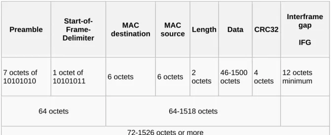
The Ethernet frames are transmitted following the scheme showed in table 3.1.
Table 3.1. Ethernet Frame configuration
Preamble
source Length Data CRC32
Interframe
64 octets 64-1518 octets
72-1526 octets or more
MII interface
The IEEE 802.3 standard defines the design and configuration of specific purpose
systems that implements the MII interface. For this project, the DP83848 card of
National Instruments[
1] was chosen.
This card has a serial management interface that is accessible through two pins,
the Management Data Clock (MDC) and the Management Data Input/Output
(MDIO). The MDC has a maximum operation frequency of 25 MHz and doesn’t
have a minimum one. The MDIO is a bidirectional line that may be used to
1
The datasheet of the DP83848 National Instruments Card is shown in the ANNEX 2.
configure the MII interface through the writing of the Basic Mode Control Register
(BMCR) and it’s also used to obtained the link specifications through its reading.
Forward Error Correction (FEC)
Generalities and Formulation
This is a control error system for data transmission, in which redundant data are
generated and concatenated at the end of the transmitted sequence. It allows,
according with the algorithm implemented, the detection and correction of a limited
number of errors that may be present on the receiver side. This method is usually
applied in communication systems in which the retransmission is impossible.
The Reed Solomon is an error correcting algorithm commonly employed on the
FEC encoding/decoding implementation. Basically, it over samples the data
sequence that has to be transmitted and generates over-determined polynomial
values that are sent. The over sampling gives to the receiver the capacity to
recover the correct values of the erroneous data when decoding.
The mathematical formulation of this algorithm is as follows:
Given a finite field F (also referred as Galois Field) and polynomial ring F[x], let n
and k be chosen such that 1
≤
k
≤
n
≤
| F |. Pick n distinct elements of F, denoted
{ x
1, x
2, ... , x
n}. Then, the codebook
C
is created from the tuplets of values
obtained by evaluating every polynomial (over F) of degree less than k at each x
i;
that is,
dimension k and minimum distance n-k+1.
Hardware Implementation
The hardware implementation of the Reed Solomon Encoder and Decoder are
explained by their respective datasheets[
1].
4 Methodological
Procedures
4.1 Problem Definition
The problem definition was based on interviews and meetings with the POF-ALL
research team.
4.2 Investigation and Solution Synthesis
The problem definition and the system design were developed base on interviews
with the PhotonLab researchers. For the development and implementation of the
system, the Xilinx and Nallatec[
2] manuals were consulted.
4.3 Solution Implementation
The procedure followed to implement the solution involves the following steps
First Stage: MII Implementation
Investigation:
This activity involves the familiarization with the IEEE/802.3/ETHERNET protocol,
specifically with the MII interface. It also includes the learning of VHDL language,
since this is the established language for the whole project.
Configuration of the MII interface:
Implement the MII configuration system in an FPGA using VHDL on Xilinx ISE
Foundation 8.1.03i.
Simulation of the MII:
In this activity the behavioral and “post place and route” simulations with
Modelsim® edition 6.0d. took place.
Testing of the MII:
Once the MII configuration system was simulated, it was tested for the different
data rates required. The tests performed are detailed in Appendix A.3.
Second Stage: Test Unit and Transmitter Implementation
At this stage the field test architecture and the transmission module that treats the
data received from the MII interface were design and implemented.
Investigation:
Familiarization with the Cores provided by Nallatech and Xilinx that were used in
the implementation of the hardware architecture.
Programming:
The system was designed and implemented in a FPGA using VHDL on Xilinx ISE
Foundation 8.1.03i.
Simulation:
In this activity the behavioral and “post place and route” simulations with
Modelsim® Xilinx edition 6.0d. took place
Testing of the system:
22
5 Description of the Selected Solution
5.1 Hardware Description
5.1.1 Hardware General Description
Figure 5.1 shows the general diagram of the hardware implementation of the
selected solution. The details regarding the implementation of each module are
given in the following sections. However, at this point the main generalities of the
system are explained.
MDC
5.1.2 MII Initialization System
The configuration system of the card that implements the MII interface is part of
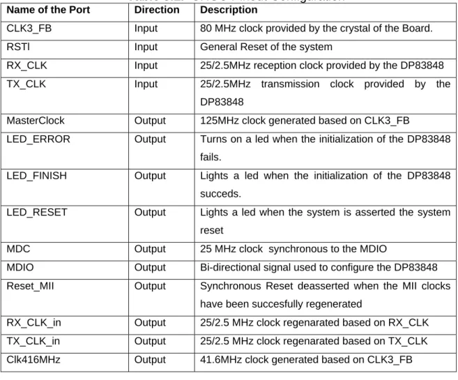
the module called Clocks and Resets Generation Unit (CRGU). This module is
also in charge of the logic resets and of the system’s clocks. Figure 5.2 shows its
block diagram and the table 5.1 describes its port connections.
Table 5.1. CRGU Pinout Configuration
Name of the Port Direction Description
CLK3_FB Input 80 MHz clock provided by the crystal of the Board.
RSTl Input General Reset of the system
RX_CLK Input 25/2.5MHz reception clock provided by the DP83848
TX_CLK Input 25/2.5MHz transmission clock provided by the
DP83848
MasterClock Output 125MHz clock generated based on CLK3_FB
LED_ERROR Output Turns on a led when the initialization of the DP83848
fails.
LED_FINISH Output Lights a led when the initialization of the DP83848
succeds.
LED_RESET Output Lights a led when the system is asserted the system
reset
MDC Output 25 MHz clock synchronous to the MDIO
MDIO Output Bi-directional signal used to configure the DP83848
Reset_MII Output Synchronous Reset deasserted when the MII clocks
have been succesfully regenerated
RX_CLK_in Output 25/2.5 MHz clock regenarated based on RX_CLK
TX_CLK_in Output 25/2.5 MHz clock regenarated based on TX_CLK
Clk416MHz Output 41.6MHz clock generated based on CLK3_FB
5.1.2.1 Second Level Diagram
Figure 5.3 shows the second level diagram of the CRGU module. The initPHY
block configures the DP83849 card. Once the MII interface is successfully
configured this block asserts its FINISH output, allowing the operation of the
CRGU_MII block and hence the generation of both the internal MII clocks and the
internal reset.
Fig.5.3. CRGU Second Level Diagram
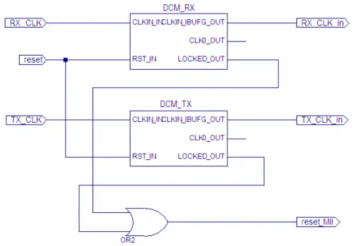
5.1.2.2 Third Level Diagram
Module CRGU_MII
The figure 5.4 shows the hardware implementation of the CRGU_MII. The two
bigger blocks (DCM_TX and DCM_RX) correspond to the Xilinx’s Core named
Digital Clock Manager (DCM)[
1], which basically allows the clock synthesis,
phasing and synchronization based on its input clock signal. The reset logic is
generated by the OR function of the LOCKED outputs of the DCMs that are
asserted high when the generated clocks are stable.
1
For further information, regarding the DCM operation, can be consulted the Virtex 4 Family Datasheet shown in the ANNEX 4
Fig.5.4. CRGU_MII Third Level Diagram
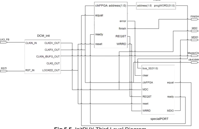
Module initPHY
Figure 5.5 shows the third level diagram of this module. It shows the minimum
system architecture developed to configure the DP83848 National Instruments
Card. The module controlGEN constitutes the CPU of the system, the ROM
memory (whose truth table is shown in the table 5.2) stores the programming
words and finally the module called specialPORT executes the communication
with the card through the bidirectional serial line (MDIO).
CLK3_FB
Fig.5.5. InitPHY Third Level Diagram
Table 5.2. Truth Table of the ROM
Address (2:0) progWORD (31:0)
000 MDIO initializing word
001 100Mbps programming word
010 100Mbps verifying word
011 Empty Position
100 MDIO initializing word
101 10Mbps programming word
110 10Mbps verifying word
111 Empty Position
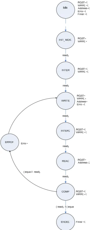
Figure 5.6 shows the state machine that controls the configuration of the MII
interface. It’s important to notice that when the card is not successfully initialized
30
5.1.3 Transmission System
The transmission block is part of a system that treats the data provided by the MII
interface in order to send them through the Plastic Optical Fiber (POF). The next
sections explains the design that handles the data up to the point at which is sent
to the pulse modulator as a 8-PAM (Pulse Amplitud Modulation) modulated
symbol. Figure 5.7 shows the first level diagram of the implemented module and
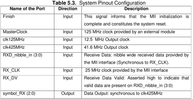
table 5.1 describes its port connections.
5.1.3.1 First Level Diagram
Finish
Table 5.3. System Pinout Configuration
Name of the Port Direction Description
Finish Input This signal informs that the MII initialization is complete and constitutes the system reset.
MasterClock Input 125 MHz clock provided by an external module clk125MHz Input 12.5 MHz Output clock
clk425MHz Input 41.6 MHz Output clock
RXD_nibble_in (3:0) Input Receive Data: nibble wide received data provided by the MII interface (Synchronous to RX_CLK).
RX_CLK Input 25 MHz clock provided by the MII interface
RX_DV Input Receive Data Valid: Asserted high to indicate that valid data are present on RXD_nibble_in (3:0)
symbol_RX (2:0) Output Data Output: synchronous to clk425MHz
5.1.3.2 Second Level Diagram
The transmission block is composed by five fundamental sub-blocks, that from
now on, will be referred as A,B,C,D and E. The location of the synchronization
interfaces was the criterion applied to define the functional blocks in the logic
chain. This means that each block is separated from the next one by a
synchronization interface, which is implemented with a special circuit involving
asynchronous FIFO. The next sections explain the main characteristics of these
Blocks and the connections between them.
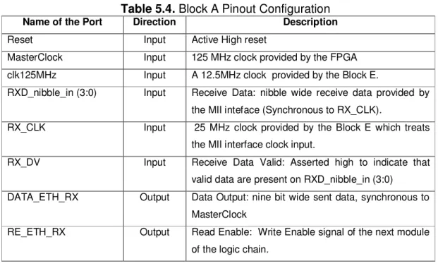
Block A: word and Inter Frame Gap codification.
Clock Generalities
Block A works with two different clock domains. At the input, the data received
(RX_nibble_in (3:0)) are synchronized with RX_CLK (25 MHz), which is provided
32
Operation
The module concatenates two samples of RX_nibble_in (3:0) in order to form a
byte. Then, it adds RX_DV and forms a 9 bit data word that is assigned to
DATA_ETH_RX (8:0). This output will be valid data when RX_DV is asserted high,
or on the contrary, an Inter Frame Gap (IFG). The encoding of the IFG is
necessary because the system must generate it on the other side of the POF in
order to fulfill the ETHERNET protocol. There are two IFG’s encoding words to
foresee the effect of the encoded data on the communication line due to the DC
Balancing[1]. The table 5.4 describes its port connections.
Fig.5.8. BLOCK A block diagram.
1
Table 5.4. Block A Pinout Configuration
Name of the Port Direction Description
Reset Input Active High reset
MasterClock Input 125 MHz clock provided by the FPGA clk125MHz Input A 12.5MHz clock provided by the Block E.
RXD_nibble_in (3:0) Input Receive Data: nibble wide receive data provided by the MII inteface (Synchronous to RX_CLK).
RX_CLK Input 25 MHz clock provided by the Block E which treats the MII interface clock input.
RX_DV Input Receive Data Valid: Asserted high to indicate that valid data are present on RXD_nibble_in (3:0)
DATA_ETH_RX Output Data Output: nine bit wide sent data, synchronous to MasterClock
RE_ETH_RX Output Read Enable: Write Enable signal of the next module of the logic chain.
Block B: IDLE insertion
Clock Generalities
This block is simpler than the previous one, because it just works with the
MasterClock at 125 MHz (see fig.5.9).
Operation
The system works with the premise that there must always be data flow in the
logic chain, but this is impossible considering that the data from the MII are
sampled with a 25 MHz clock whereas the data in the chain are transmitted with a
125 MHz. Then is necessary to include special data words in order to avoid the
absence of real data. These words are referred as IDLE’s. Again, there are two of
them because of the DC balancing consideration. The module inserts these words
when the SER_FLAG signal is asserted high by a logic that detects the moment at
34
The insertion of these words also generates the necessity of a synchronization
and storage circuitry, since is necessary to store them while all the signals needed
for their transmission are generated, and also in order to accumulate them to
maintain the data flow.
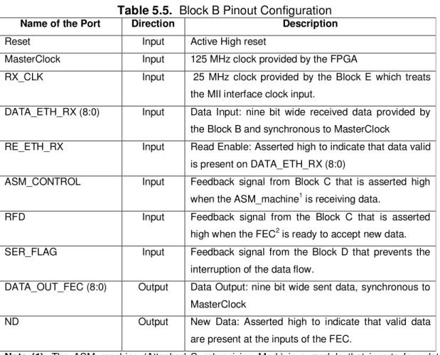
Table 5.5. Block B Pinout Configuration
Name of the Port Direction Description
Reset Input Active High reset
MasterClock Input 125 MHz clock provided by the FPGA
RX_CLK Input 25 MHz clock provided by the Block E which treats the MII interface clock input.
DATA_ETH_RX (8:0) Input Data Input: nine bit wide received data provided by the Block B and synchronous to MasterClock
RE_ETH_RX Input Read Enable: Asserted high to indicate that data valid is present on DATA_ETH_RX (8:0)
ASM_CONTROL Input Feedback signal from Block C that is asserted high when the ASM_machine1 is receiving data.
RFD Input Feedback signal from the Block C that is asserted high when the FEC2 is ready to accept new data. SER_FLAG Input Feedback signal from the Block D that prevents the
interruption of the data flow.
DATA_OUT_FEC (8:0) Output Data Output: nine bit wide sent data, synchronous to MasterClock
ND Output New Data: Asserted high to indicate that valid data are present at the inputs of the FEC.
Note (1): The ASM_machine (Attached Synchronizing Mark) is a module that inserts four data words at the beginning of each transmission in order to synchronize its decoding on the other side of the POF, this function is part of the next block and is explained in the corresponding section.
36
Block C: ASM insertion and FEC generation.
Clock Generalities
This block works with the MasterClock (125 MHz).
Operation
This module implements the Forward Error Correction (FEC). The sequence is
constituted by 479 information words (9 bits codification) and 32 verification words,
generated applying the Reed Solomon algorithm[1]. Each sequence is preceded
by four special words called ASM, which are needed to synchronize the data
acquisition in the module located on the other side of the POF. In figure 5.10 the
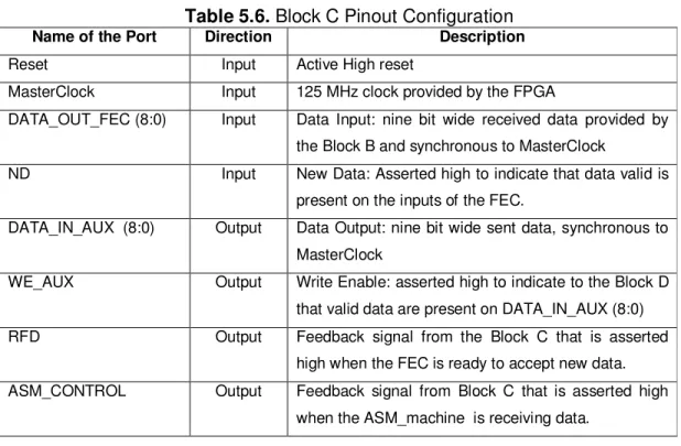
block diagram of the block C is shown and table 5.6 describes its port connections.
.
Fig.5.10. BLOCK C block diagram.
1
Table 5.6. Block C Pinout Configuration
Name of the Port Direction Description
Reset Input Active High reset
MasterClock Input 125 MHz clock provided by the FPGA
DATA_OUT_FEC (8:0) Input Data Input: nine bit wide received data provided by the Block B and synchronous to MasterClock
ND Input New Data: Asserted high to indicate that data valid is present on the inputs of the FEC.
DATA_IN_AUX (8:0) Output Data Output: nine bit wide sent data, synchronous to MasterClock
WE_AUX Output Write Enable: asserted high to indicate to the Block D that valid data are present on DATA_IN_AUX (8:0) RFD Output Feedback signal from the Block C that is asserted
high when the FEC is ready to accept new data. ASM_CONTROL Output Feedback signal from Block C that is asserted high
when the ASM_machine is receiving data.
Block D: Data serialization
Clock Generalities
This module works with two clocks, the first one is the MasterClock (125MHz),
used to sample the data present at its inputs and the second one is the clk425MHz
used to serialize the data words into symbols constituted by three bits.
Operation
This module samples its input DATA_IN_AUX (8:0) when WE_AUX is asserted
high by the preceding module. This operation is realized in synchrony with
MasterClock. Once received, the data word is divided into three symbols,
constituted as well by three bits of data. This serialization is made using
clk425MHz (41.6MHz). In the end these symbols are sent to the 8-PAM modulator
38
Fig.5.11. BLOCK D block diagram.
Table 5.7. Block D Pinout Configuration
Name of the Port Direction Description
Reset Input Active High reset
MasterClock Input 125 MHz clock provided by the FPGA
Clk425MHz Input Serialization Clock: a 41.6 MHz clock generated inside the FPGA by the Block E in order to serilize the data words sampled in DATA_IN_AUX.
DATA_IN_AUX (8:0) Input Data Input: nine bit wide received data provided by block C and syncronous to MasterClock.
WE_AUX Input Write Enable: asserted high to indicate to the Block D that valid data is present on DATA_IN_AUX (8:0) Symbol_RX (3:0) Output Data Output: three bit wide output data sent to the
8-PAM modulator and synchronous to clk425MHz. SER_FLAG Output Feedback signal sent to the block B in order to avoid
40
5.1.4 Testing System of the Media Converter
This system is used to execute the field tests of the Media Converter constituting a
fundamental part of its debugging process. The test procedure is as follows:
1) Disable the MII interface as a data source.
2) Isolate the modules that will be tested configuring an internal loop
connection in an appropriate point.
3) Transmit a Pseudo Random Binary Sequence (PRBS) through the
prototype.
4) Download the data sequence received into a computer.
The testing system is composed by a Traffic Generation Unit (TGU), a Data
Compilation Unit (DCU), a downloading interface (see figure 3.1), and a State
Machine that controls the data transfer between the modules mentioned and the
computer. These blocks will be explained in the next sections.
5.1.4.1 Traffic Generation Unit TGU
This module generates the PRBS that is transmitted through the Media Converter.
Due to the intrinsic complexity of the implementation of a PRBS generator, the
sequence was created with Matlab and uploaded into a ROM inside the PFGA
using a Xilinx Core Tool. Nevertheless, this solution implied the use of a large
ROM which had an obvious impact on the system efficiency. So at this point, was
decided to generate a PRBS composed by 6554 words 5 bits wide and transmit it
continuously until a larger DCU’s memory is filled. Figure 5.13 shows the hardware
configuration of the TGU. It’s important to mentione that the counter’s pin called
Count Enable (CE) is employed by the Control Unit to enable/disable the PRBS
Fig.5.13. Traffic Generation Unit Diagram
5.1.4.2 Data Compilation Unit DCU
DCU First Level Diagram
The information is stored by the DCU once it passes through the media converter.
The FIFO_OUT width was defined according to the Downloading Unit
requirements, which is based on a core provided by Nallatec. Figure 5.14 shows
the DCU first level diagram and the table 5.8 describes its port connections.
42
Table 5.8. DCU Pinout Configuration
Name of the Port Direction Description
Reset_MII Input Reset provided by the CRGU
TX_CLK_in Input 25MHz clock generated based on TX_CLK
FIFO_RCLK Input 40MHz clock provided by the Downloading Interface FIFO_REN Input Read Enable: connected to the downloading
interface.
DCU_TX_DATA Input Data Input: 32 bits wide word synchronous to TX_CLK_in
FIFO_WEN Input Write Enable: Asserted High by the Control Unit to write a 32 bit word into the Internal FIFO.
Shift Input Asserted High by the Control Unit to process a new PRBS symbol.
FIFO_OUT (31:0) Output Data Output: 32 bits wide word synchronous to FIFO_RCLK
TRANSFER_COMPLETE Output Asserted High to Indicate to the Downloading Unit that the DCU’s FIFO is full and ready to transfer the data collected.
FIFO_EMPTY Output Asserted High to indicate to the Downloading Unit that the DCU’s FIFO is empty.
TRACK Output Asserted High to indicate to the Control Unit that the sequence that preceeds a new transmitting process has been detected.
FIFO_FULL Output Asserted High to indicate to the Control Unit and to the downloading interface that the DCU’s FIFO is full.
Second Level Diagram
This unit is composed by a concatenation module and a 16Kbyte FIFO. Figure
5.15 shows its hardware configuration. The next sections will explain the operation
of each module.
Fig.5.15. DCU Second Level Diagram
Concatenation Module
This module takes the 5 bit PRBS symbols and concatenates them in order to
form a 32 bit word that is stored into DCU_FIFO. This process is performed while
“shift” corresponds to a logic one. Moreover, it recognizes the synchronization
sequence at the beginning of each transmission, communicating it to the Control
Unit through its pin labeled as TRACK.
DCU_FIFO
This is a 16Kbytes memory block that stores the data words received from the
44
5.1.4.3 Control Unit
Figure 5.16 shows the states diagram of the Control Unit.
5.1.4.4 Download Unit
This module has been implement using the PCI communications Core developed
by Nallatech. It can establish communication between the computer and the FPGA
by means of two different interfaces, the first one is a Memory Map interface and
the second one is a DMA interface, it also can be configured by software to use
the USB port instead of the PCI bus, which facilitates the board connection to the
computer.
For this project the communication through the DMA interface has been configured
and established using the USB as communication port with the PC. Figure 5.17
shows the block diagram of the core and the table 5.9 describes its pinout
46
Table 5.9. Core Pinout Configuration[1]
Signal Description Width Description
EMPTY INPUT 1 Indicates that PCI FPGA has data to transfer
BUSY INPUT 1 Indicates that PCI FPGA can receive data AS/DS# INPUT 1 Determines if data from PCI FPGA is
address or data (LOW indicates Data) RST# INPUT 1 Reset signal from PCI FPGA (Active ADDRESS INPUT/OUTPUT 31 Address for memory map interface DMA_ENABLE OUTPUT 1 Indicates that DMA interface is enabled DMA_DIRECTION OUTPUT 1 Indicates direction of DMA interface
(LOW indicates data from core to user design, HIGH data from user to core) DMA_DATA_AVAILABLE OUTPUT 1 Indicates the DMA interface has data for
user design
DMA_REN INPUT 1 Read enable to read data from DMA interface
DMA_RDY OUTPUT 1 Indicates the DMA interface is ready to receive data from user design
DMA_WEN INPUT 1 Write enable to write data to the DMA interface
DMA_DATA INPUT/OUTPUT 32 Data for DMA interface
COUNT OUTPUT 32 DMA count. Counts down from number of words to transfer down to zero
DMA_SEL OUTPUT 4 Selects one of sixteen DMA channels
DMA Interface Configuration
The PCI Communication Interface has two internal register that controls the DMA
interface: the DMA Control/Status Register (Address 0x00000000) and the DMA
count Register (Address 0x00000001). These registers must be initialized before a
transfer begins and must be cleared after it has finished. The initialization and
configuration of this interface is achieved by software, using the C++ programs
and libraries developed by Nallatech. Further information regarding the DMA
hardware configuration can be consulted on the datasheet included in Annex 3.
5.1.5 Reconstruction of the Preamble
Once the modules explained in the previous sections were programmed, took
place first attempts to assemble the system. The connection of the first blocks
revealed the existence of a problem regarding the reception of the information
from the MII interface.
A loopback was connected to the DP83849 national card and several PING
transmitting sequences were executed in order to determine what the problem
was. In the end it was determined that during clock synchronizing the card
discarded 1 to 10 bits of the beginning of the ETHERNET frame. The lost bit
corresponded to the Preamble of the frame, hence it was necessary to implement
an interface in charge of its reconstruction.
The system implemented generates a new preamble for each ETHERNET
sequence received. It has a control unit that responds to the Start of Frame
Delimiter (SFD) interrupting the sequence and sending 15 preamble nibbles
48
Fig.5.18. State Diagram of the Control Unit
Figure 5.19 shows the hardware implementation of this system. It’s important to
notice the presence of the FIFO memory, which is used to store the data while the
50
5.2 Software Description
A C++ application programs the FPGA and the DMA interface, then it controls the
data transfer and finally it generates the .txt file required by Matlab to compare the
received sequence with the transmitted sequence in order to verify the proper
operation of the media converter.
The libraries developed by Nallatech were used[1] both to program the board and
to execute the data transfer. The program code can be consulted in the appendix
A.5, the flow diagram showed in the figure 5.20 explains the sequence executed
by the software in order to download the information.
1
52
Table 6.1 Results obtained from TEST1
Result Obtained Tested Action
First Attempt Second Attempt
The system continuously executed the initialization sequence of the DP83848
The system initialized properly the DP83848
X
Table 6.1 shows that the reprogramming sequence executed by the MII
initialization System worked as expected. The BMCR register was programmed
successfully every single time. However, the reading process presented some
problems on the first test, because the system retried the initialization process
despite the fact of being properly configured. At this point a Logic Analyzer was
used to monitor the MDIO signal finding that the given time between transfers
didn’t fulfill the minimum value specified by the DPC83848C datasheet. Thus, a
module to generate a delay was included; further tests showed that the MII
Interface is initialized without any problem.
The table 6.2 shows the results obtained when the TEST 2 (see procedure in
Appendix A.4) was performed.
Table 6.2 Results obtained from TEST2
Result Obtained Tested Action
First Attempt
The system initialized properly the DP83848 at a 10Mbps
The system initialized properly the DP83848 at a 100Mbps
Table 6.2 demonstrate that the configuration given to the DPC83948 card allows
Figure 6.1 shows the summary of the first PING that was executed in the TEST 3
(see procedure in the Appendix A.4).
Fig.6.1. PING summary in the Command Prompt
Figure 6.1 shows that when the TEST 3 was performed, 1% of the PING packages
were lost. Hence, a Logic Analyzer was used to determine what the problem was.
At the end it was discovered that, during clock synchronizing, the card discarded 1
to 10 bits of the preamble. This problem was solved with the implementation of the
Preamble Reconstruction Block; the results obtained are shown in the figures 6.2
54
Fig.6.3. PING summary in the Command Prompt
Testing System of the Media Converter
The TEST4 showed that the PRBS sequence downloaded into the PC presented
differences with the sequence transmitted, see table 6.3.
Table 6.3. Error Positions and number of bits lost in a PRBS of 32767 bits long
Error Position Number of bits lost
870 10
3705 15
8525 15
Lost Bits (%) 0.122
In order to solve this problem all the software algorithms implemented were
analyzed and tested. This task implied the use of the step by step debugging tool
included in the C++ editor environment.
Once the possibility of a software error was discarded, the analysis of the
hardware took place. The DMA interface was isolated with the connection of a 32
bit counter to generate a sequence that could be verified using step by step
debugging tool in real time operation. This test helped to determine that the
6.3 shows the position and the quantity of bits lost, concluding that 0.122% of the
information is lost through the downloading process. The Nallatech interface was
composed of an Asynchronous FIFO with a 16x32 bits capacity and a Control Unit.
The internal FIFO was replaced with an Asynchronous FIFO generated with the
Xilinx Core generator. The test was repeated several times with FIFOs of 32, 64,
128 and 1024 words capacity. However, the errors were present at the same
positions, consequently it was concluded that the problem wasn’t provoked by an
overflow error in the FIFO.
At this point it was considered to modify the Control Unit, but this module was
provided by Nallatech as a “Black Box”, making impossible to change its logic
design and hardware implementation. The programming of a new interface wasn’t
possible either, because the USB interface works with the C++ Nallatech Libraries
and the protocol followed for the port management and initialization isn’t specified
by the provider.
The impossibility to correct the data lost in the downloading process implied the
evaluation of other solutions. At the beginning the use of the same downloading
interface jointly with a module that would locate the number of errors and its
positions in the sequence was considered. The downloading process wouldn’t be
a problem because the first bit lost is located at position 870, which means that
27x32bit words could be received in the computer without the presence of errors.
In other words, this solution would allow the location of 32 bit errors with their
respective positions in the sequence. Nevertheless, the incapability to isolate more
than 32 errors and the inherit complexity of the module needed to locate and
generate the report didn’t accomplished the simplicity and small space
consumption required for the implementation of the internal Testing Unit. Thus, it
56
design and implementation of the analog circuits needed to convert the TTL levels
voltage into RS232 levels voltage. Moreover, regarding the software, it was
necessary to program an application to receive and generate the errors report as a
.txt file. These facts and the RS232 obsolescence lead to the conclusion that this
wasn’t either the bestanswer to the problem.
At last, considering the simplicity, hardware size, effort and time implementation, it
was decided to use the same downloading interface, but considering the bits lost
(see table 6.3) in the information analysis. The test configuration may be seen in
the figure A.5 in the Appendix A.5.. Hence, it was recommended to program a
MatLab application to remove the bits lost from the original PRBS in order to
compare it later with the downloaded PRBS, with the advantage that this solution
doesn’t limit the number of findable error bits and doesn’t need further hardware
resources from the FPGA.
FPGA Utilization
Figure 6.4 shows the FPGA Virtex IV utilization percentages.
Fig.6.4. FPGA Utilization
This summary shows the minimum requirements needed to implement the Media
Fig.6.5. Timing Summary of the Media Converter
Figure 6.5 shows that the maximum clock frequency of the Media Converter is
171.223MHz. This means that the system could add more control words or even
more logic levels without affect the ETHERNET data rate. This figure also shows
that the Media Converter has an input constraint of 5.484ns and an output
constraint of 6.465ns. This information is useful for the interaction of the Media
7 Conclusions and Recommendations
7.1 Conclusions
• The Media Converter is capable to establish Fast Ethernet Communication
both at 100Mbps and at 10Mbps.
• The Media Converter counts with two possible test methodologies and their
respective hardware, the first one uses the Fast Ethernet Link as a data
source, collecting the results with the network monitoring Tools embedded
on Windows. The second one consists on the internal emulation,
transmitting, receiving and downloading of a PRBS that is verified with
Matlab.
• The Media Converter uses a 4% of the total slices of the FPGA Virtex IV.
• The Media Converter minimum FPGA requirements are: 706 Flip Flops,
1108 LUTs (Look Up Tables) with 4 input (964 used as logic and 144 used
as RAM, random access memory), 108 bonded IOBs (Input/Output Blocks),
12 FIFO16/RAMB16s, 9 GCLKs (Gated Clocks) and finally 4 DCMs.
• The Media Converter has maximum combinational path delay of 6.539ns,
and a Maximum Clock frequency of 171.223MHz.
• The Media Converter has an input constraint of 5.484ns and an output
60
7.2 Recommendations
• The main recommendation is to use both testing methods in the Media
Converter depuration process, because the Internal Testing Unit allows to
debug the system, whereas the establishment of Fast Ethernet
Communication validates the implementation of the system as a
commercial product compatible with a worldwide standard.
• Request to Nallatech a debugged version of its PCI communications Core.
Specify the presence of errors and their positions when the interface is
configured to execute DMA transfers through the USB port of the Nallatech
card. Also inform that it was concluded that the error is located in the
Control Unit of the Core. Finally, explain that error location was deduced
based on the lack of satisfactory results when hardware modifications were
made to the other modules inside the Core.
• Acquire specialized network analysis software in order to generate statistics
to validate the system. This software should have access to a set of
capabilities and analysis variables such as:
1. An accurate calculation of the data lost percentage.
2. The number of resending processes and the time needed to send
the data.
3. Operation time with error free and consequently the error frequency
to determine its possible periodicity.
4. A debugging tool capable of emulate Ethernet information from an
algorithm or file given by the user. This feature could allow the
transmission of a more complex PRBS directly to the MII interface
and later to the system, which could be an alternative to the Internal
8 Bibliography
[1] CrossLink, “The Aerospace Corporation Magazine of advances in aerospace
technology” [online]. Includes an article that explains the FEC.
< http://www.aero.org/publications/crosslink/winter2002/04.html>
[2] WIKIPEDIA, “The Free Encyclopedia” [online]. Optical Fibers.
< http://en.wikipedia.org/wiki/Optical_fiber>.
[3] Mouse Home Page, “The Radio Network Processor” [online]. Includes a section
regarding the Reed Solomon Algorithm with several articles and related documents.
< http://www.radionetworkprocessor.com/reed-solomon.html>.
[4] POF ALL Association, Internet Site [online]. Plastical Optical Fiber.
< http://www.pofac.de/pofac/en/what_are_pof/step_index.php>.
[5] Daum,W.;Krauser. J.; Zamzow, P.; Ziemann,O.Polymer Optical Fibers for
Data Communication . Germany, Springer-Verlag Berlin Heidelberg, 2002.
[6] Nallatech. XtremeDSP Development Kit-IV User Guide.Nallatech Limited,
2005.
[7] Spurgeon, Charles E..Ethernet: The Definitive Guide . First Edition, O’Reilly
62
9 Appendix
A.1 Glossary, abbreviations and Symbols
A
ASM: Attached Synchronizing Mark
B
BMCR: Basic Mode Control Register
C
CRGU: Clock and Reset Generation Unit CPU: Central Processing Unit FIFO: First In First Out
FPGA: Field Programmable Logic Array
G
GCLK: Gated Clock
H
HDL: Hardware Description Language
I
M
MAC: Medium Access Controller MDC: Management Data Clock
MDIO: Management Data Input/Output MII: Media Independent Interface
O
OSI: Open System Interconnection
P
PAM: Pulse Amplitud Modulation
PCI: Peripheral Component Interconnect
PHY: Physical Layer of the OSI Reference Model POF: Plastic Optical Fiber
POF-ALL: Paving the Optical Future with Affordable Lightning-fast Links PRBS: Pseudo Random Bit Sequence
R
64
S
SFD: Start Frame Delimiter
T
TGU: Traffic Generation Unit
U
USB: Universal Serial Bus
V
A.2 Company Information
PhotonLab is a 250 square meters laboratory constituted by different work areas,
such as the optical system and network experiment area, an electronics lab, a
dark room, a filtered air system in a class 1000 clean room and a special design
that isolates it from external vibration. Furthermore, this facility is equipped with
test and measurement equipment, several BER tester (12.5 Gbit/s and 40Gbit/s),
50 GHz oscilloscopes, optical spectrum analyzers, electrical and optical network
analyzers up to 40 GHz, numerous optical and electro-optical components and
66
A.3 Testing Procedures
This section explains the field tests performed to verify the proper operation of the
systems implemented. The FPGA was programmed using the software provided
by Nallatech.
TEST1
The figure A.1 shows the setup of the test performed in order to verify the
programming system that initializes the MII interface.
Fig.A.1. Test 1 Configuration
Test procedure:
1) Connect the Reset jumper of the DP83848C.
2) Start the programming sequence with the FPGA.
3) Verify that the programming system execute continuously the initialization
sequence.
4) Remove the Reset jumper of the DP83848C.
TEST 2
The figure A.2 shows the set up of the test performed to the MII interface in order
to verify its capacity to establish the link specifications.
Fig.A.2. Test 2 Configuration
Test Procedure:
1) Configure the computer link at 100 Mbps and with the auto-negotiation
capability.
2) Program the DP83848C at 10Mbps without the auto-negotiation capability.
3) Check with the Windows Network Tools the reconfiguration of the computer
link due to the auto-negotiation process.
This test was performed configuring the PC link at 10Mbps and the card at
68
TEST 3
The figure A.2 shows the set up of the test performed in order to verify the
reliability of the data transmission and receiving through and from the MII
interface. It was performed to corroborate the proper operation of the Internal
Testing System in the FPGA.
Test procedure:
1) Program the DP83848C at 10Mbps without the auto-negotiation capability.
2) Execute a PING from the PC1.
3) Wait the answer from PC2.
TEST4
The figure A.4 shows the set up of the test performed in order to verify the testing
system implemented inside of the FPGA .
Fig.A.4. Test 4 Configuration
Test procedure:
1) Disable the MII Interface as a data source.
2) Configure the DP83848C.
3) Start the testing transmission inside the FPGA.
4) Download the PRBS sequence into the PC.
70
A.4 Testing Set up with the POF as loopback
MDIO/MDC
DP83848C PHYTER FPGA
USB
POF
A.5 C++ Programming Code of the Software Application
The following lines show the libraries inclusion, the DWORD global variables
declaration, the programming files assignment and finally the local variables
72
At this point the communication with the FPGA is established, the Card
specifications are obtained and it’s opened in order to initiate the programming
Once the card is opened, the program enables the resets, sets the clocks,
74
Subsequently the DMA configuration and the downloading process takes place.
At this point is opened the .txt file, and begins the writing process, which implies
This is the method that converts the data downloaded from DWORD to binary,
76
The next method converts the data contained in printDATA from binary to double
allowing its printing in the .txt file.
10 Annex
ANNEX 1 Photos of the cards and devices utilized to implement
the system
.DP83848 National Instruments Card
78
80
82
84