beyond 32 nm
Lourdes Pelaz,a兲 Luis A. Marqués, María Aboy, Iván Santos, and Pedro López Universidad de Valladolid, Campus Miguel Delibes, 47011 Valladolid, Spain
Ray Duffy
NXP-TSMC Research Center, Kapeldreef 75, 3001 Leuven, Belgium
共Received 15 June 2009; accepted 24 August 2009; published 1 March 2010兲
Ion implantation continues being the dominant technique to introduce dopants in Si devices. With the device feature size in the nanometer scale, the accurate and detailed description of as-implanted dopant and damage profiles is becoming key as advanced annealing techniques are almost diffusionless. The demanding requirements for ultrashallow junction formation are stimulating the development of improved and detailed models for molecular implants and for the kinetics of amorphous damage. Additional challenges arise in the doping of advanced architectures, such as fin field effect transistors, because the introduction of highly tilted ions is quite inefficient and, in addition, the regrowth of amorphous regions in narrow structures is hampered by the slow regrowth
at free interfaces and 兵111其 planes. Atomistic simulations play a relevant role to provide the
understanding for the development of simplified physically based models computationally more
efficient. © 2010 American Vacuum Society. 关DOI: 10.1116/1.3231481兴
I. INTRODUCTION
As devices are scaled down, it is becoming more and more challenging to keep a good control of short channel effects共SCEs兲with simultaneous high drive currents and low off-state leakage.1At the junction level, the need to control SCE has motivated the progressive reduction in junction depth at the source and drain共S/D兲extensions. Junctions are generally formed by ion implantation as this is a conven-tional and well established technique. The formation of ul-trashallow junctions is particularly challenging in the case of B because its low mass demands the use of ultralow energy implants. Molecular implants with B18H22ions have proven
to be advantageous for ultrashallow junction formation be-cause higher extraction energy can be used while the effec-tive energy per B ion is scaled by the number of B atoms in the molecule.2In addition, the damage created by this heavy molecule causes self-amorphization, saving the preamor-phization implant step required when monoatomic B is used to take advantage of solid-phase epitaxial regrowth共SPER兲. The maximization of drive current for higher switching speed demands a minimization of access resistance. This re-quirement has driven the development of strain technologies to enhance carrier mobility3 and the use of SPER and milli-second anneals to achieve maximum dopant activation with
minimal diffusion.4 However, the presence of residual
de-fects after regrowth is a pressing concern as they can cause additional leakage, limiting low power applications. The re-moval of these defects generally requires high thermal bud-gets, which causes the spreading of the junction depth, and therefore, deteriorates SCE control. The difficult trade-off between shallow junction formation, maximum dopant acti-vation, and defect removal becomes more and more
chal-lenging as the gate length is reduced further in each
technol-ogy node.1To be able to maintain a good SCE control while
fulfilling other device requirements, the International Tech-nology Roadmap for Semiconductors foresees a transition from traditional planar silicon metal oxide semiconductor 共MOS兲field effect transistors to ultrathin-body fully depleted MOS devices in the near future and to alternative device architectures, such as fin field effect transistors共FinFETs兲, at
the 22 nm node and beyond.1The incorporation of materials
with very high carrier mobility, such as Ge and III-V com-pounds, to substitute Si in the channel of advanced device architectures is being considered for further technologies.1,5
The goal of process modeling is to provide physical un-derstanding and simulation tools to help the development and optimization of device fabrication. Therefore, the trends in device technology drive the requirements for process modeling.共i兲The continuous reduction in feature size in the devices is demanding improved models so that small varia-tions in the dopant profiles can be accurately predicted.
Ki-netic Monte Carlo 共KMC兲 methods are starting to play a
more relevant role as they can reach actual device dimen-sions and time scales typical of actual processes.共ii兲For new device architectures, it is necessary to assess existing pro-cesses and probably develop new ones to address new issues that arise in nonplanar structures. 共iii兲 The incorporation of other materials, such as Ge or III-V compounds, to substitute Si in the channel, is promoting a number of studies to estab-lish models and parameters that describe accurately the be-havior of dopants and defects in these materials during pro-cess integration in nanometer scale high speed logic devices. For the models to be able to fulfill their goal, they should be physically based and computationally efficient. Theory and dedicated experiments provide information about funda-mental mechanisms and parameters. However, the resulting models may be computationally too expensive to be
tively used for device optimization. Empirical approaches and fitting are sometimes used to develop simplified models that are computationally efficient and accurate, at least within a limited and relevant range of process parameters. Simplified models can also be extracted from the understand-ing of the most relevant mechanisms that take place through a multiscale approach.6Ab initiomethods are parameter free and include the quantum description of the atomic system, but due to its huge computational load, only a few atoms 共64–216兲are typically included in the simulations. Classical
molecular dynamics共MD兲describes the dynamics of the
at-oms based on empirical classical potentials. Although the Si–Si interaction is reasonably well described by empirical potentials,7–9 no good empirical classical potentials have been established to capture the interaction between Si and impurities. Typical simulation cells include between 103and
106 atoms, but this technique is very time consuming for
simulation times above 1 ps. It is useful to extract mecha-nisms and atomic parameters that can be used in the other less detailed techniques. Atomistic simulations that reach sizes typical of actual devices共10–100 nm兲can be performed with KMC models. Their main drawback is the large number of atomistic parameters that must be specified, most of which are difficult to extract. Continuum models are based on the resolution of partial differential equations. They are the mainstream in process simulation because they incorporate many coupled processes 共implantation, anneals, stress, oxi-dation, deposition steps, etc.兲 by using efficient simplified models.
In this article, we will provide an overview of the present status of ion implantation and annealing modeling, with spe-cial emphasis on atomistic models. By using atomistic simu-lation techniques, we will also address relevant doping issues that arise in nonplanar geometries.
II. MODELING OF ION IMPLANTATION AND ANNEALING
Ion implantation remains the stronger candidate as a mean to introduce dopants because it allows a good control of the dopant profile. However, the demanding requirements to form ultrashallow junctions are bringing about new issues. Molecular implants are being considered as a way to
intro-duce dopant atoms very close to the surface.2 Implants at
temperatures well below room temperature or at elevated temperatures are being investigated to minimize residual
damage.10 As the device dimensions are reduced and
milli-second anneals are almost diffusionless, an accurate predic-tion of the as-implanted dopant and damage profiles is be-coming more relevant. Traditionally, the emphasis lied on the
dopant profile since for nonamorphizing implants the “⫹1
model”11 or “+n model”12 were assumed for defects.
How-ever, the use of amorphizing implants followed by SPER calls for improved models for damage accumulation includ-ing damage kinetics, amorphization, and regrowth.
Although analytic functions are commonly used to de-scribe one-dimensional dopant and damage profiles in fast
continuum simulations,13 the need to properly account for
dopant fluctuations in small devices and the intrinsic two-and three-dimensional nature of advanced device architec-tures are demanding complex models to describe the implant
profiles.14A good compromise between computer efficiency
and detailed description is provided by binary collision
ap-proximation 共BCA兲-based Monte Carlo 共MC兲
simulators.15–19 BCA assumes that the energetic atom only interacts with one target atom at the time, transferring to it some of its energy. If the target atom receives more energy than a threshold value 共between 15 and 20 eV for Si兲, the atom is extracted from its lattice position, generating a Fren-kel pair 共Si interstitial and vacancy兲and starting a new re-coil. If the energy received by target atoms is lower than the threshold value, it is generally assumed to be lost to phonons. BCA-based MC simulators properly calibrated give very accurate description of dopant profiles and an accept-able description of atomistic damage created by light ions. However, for heavy and molecular ions, the complexity of the generated damage is not properly described by these
tra-ditional models.20Other BCA-based MC simulators only
fol-low the trajectory of incoming ions but not that of the recoils providing the atomic position of ions but a statistical, rather than atomistic, approach of the generated damage based on
Kinchin–Pease models.21
The detailed damage description provided by MD can be used to understand the mechanisms involved in damage
generation20,22,23 and to set the basis for simplified
models.24,25 MD calculations indicate that, in the case of light ions, the interaction between energetic ions and target atoms is mostly ballistic, resulting in a dilute distribution of Si interstitials and vacancies and very small defect clusters, as shown in Fig.1共a兲for a 0.5 keV B implant. However, the damage resulting from implants with heavy molecules, such as B18H22, is significantly different from that corresponding
to the superposition of the damage generated by individual B
cascades. For equivalent energy per B atom 共0.5 eV兲, on
average, 32 atoms are displaced with respect to their lattice positions in the case of monoatomic B implants, while in the case of B18implants, each B atom produces, on average, 108
displaced Si atoms. In this case, the main damage generation mechanism is the local melting of the region where a high amount of energy is simultaneously deposited by the B
atoms.22 This mechanism causes a huge amorphous region
共a-region兲 around the impact point, as shown in Fig. 1共b兲. These ideas derived from MD simulations have been used to
develop an improved model using the BCA-MC approach.24
The model takes into account the energy transfers below the threshold value to account for the damage generated through melting. The resulting damage is a function not only of the total deposited energy but also of the local number of atoms in which the energy is deposited. This approach provides an atomistic description of the damage generated by molecular implants, not available to the date, with only a small addi-tional computaaddi-tional load compared to tradiaddi-tional BCA
mod-els. The simulated damage generated by B18 implant using
traditional BCA and improved BCA models are compared in
Fig. 2. While traditional BCA models only produces Si
in-terstitials and vacancies corresponding to 18 overlapping B
cascades, the improved BCA model generates significantly more damage at the center of the collision cascades, as it is predicted by MD simulations.
To describe the formation of a-regions, empirical
ap-proaches assume that the lattice becomes amorphous when the concentration of point defects 共Si interstitials or vacan-cies兲 reaches a certain threshold, typically of the order of 2
⫻1022cm−3.26
This value is fitted by comparison with ex-perimental results but it depends on ion mass, implant tem-perature and ion flux as a result of the dynamic annealing of the defects during the implantation.27The different annealing behaviors of the damage generated by different ions and the kinetics of crystalline to amorphous transition has been prop-erly modeled using the bond defect or IV pair as the building block to describe the amorphous phase.26This defect, whose structure is represented in Fig. 3共a兲, is formed during ion implantation or by incomplete Si interstitial-vacancy recom-bination. It is assumed to recombine faster when it is sur-rounded by a larger number of Si atoms in crystalline lattice sites because these set a template for the lattice around the defect, favoring its recombination. The Arrhenius plot of the calculated average lifetime of isolated bond defects in a crys-talline Si matrix and bond defects at an amorphous/ crystalline interface and at a free interface is shown in Fig. 3共b兲. It indicates that bond defects at interfaces recombine over two orders of magnitude slower than isolated IV pairs in bulk. This explains the formation of near-surface a-regions with B at fluency much lower than those required to
amor-phize the volume.28 The damage generated by ultralow
en-ergy implants, even with B, can easily accumulate near the interface and extend from there. The slower recombination of bond defects at the interfaces has also consequences for the recrystallization of narrow Si layers,29,30as we will illus-trate later in the case of FinFETs.
Physically based models that properly describe mecha-nisms involved in the evolution of dopants in amorphous Si 共a-Si兲are not as well developed as they are in crystalline Si 共c-Si兲. The interaction between dopants and defects inc-Si to account for dopant enhanced diffusion and clustering is well understood and characterized, both at experimental and the-oretical levels共see Ref.31for a review兲. Detailed and sim-plified models have been developed for most common dop-ants used in Si processing. The study of dopdop-ants and FIG. 2. Binary collision approximation–Monte Carlo based simulation of the
damage generated by 18 simultaneous 0.5 keV B cascades using共a兲classical atomistic damage model that generates Si interstitials and vacancies and共b兲 improved model that includes also the additional displaced atoms due to the energy transfers below the threshold value.
FIG. 3.共a兲Structure of the bond defect or IV pair.共b兲Arrhenius plot of the calculated mean lifetime of the bond defect when it is located at in bulk
impurities, in general, ina-Si is much more complex than in c-Si. Since regrowth occurs quite fast at relatively low tem-peratures, the experimental window is quite limited, and the inherent diversity of local environments in an amorphous cell makes theoretical studies difficult. There are some em-pirical and quite simplistic models that account for some experimental observations but they lack physical basis that account for the rich phenomenological observations of dop-ants ina-Si.32,33 B diffusion and clustering has been experi-mentally evidenced in B profiles in preamorphized Si.34–36 Theoretical calculations have shown that there are some B cluster configurations that are energetically favorable to be
formed during regrowth of a-Si.37 Some models assume B
clustering as the initial condition after regrowth when the B concentration exceeds the threshold concentration of the or-der of 2⫻1020cm−3.32However, it has been experimentally demonstrated that the threshold concentration for B cluster-ing formation ina-Si increases when the regrowth occurs at high temperatures.38 Other dopants, such as As, do not dif-fuse appreciably in a-Si共Ref. 39兲 but they exhibit a strong segregation during regrowth so that the dopant profile after regrowth significantly differs from the as-implanted one.40 The incorporation of F ina-Si has been proven to be benefi-cial for ultrashallow junction formation because F-vacancy
complexes appear in the regrown layer.41 Some theoretical
calculations have demonstrated the stability of some small F-vacancy complexes,42but also rather large complexes have
been experimentally observed.43 It would be necessary to
develop physically based models that can provide the under-standing and the clues required to optimize electrically active dopant profiles when SPER is involved.
III. DOPANT INCORPORATION AND DAMAGE RECOVERY IN FINFETS
To achieve a good control of SCE and off-state leakage, the fin widths of FinFET devices must be narrow44,45but the parasitic source-drain resistance increases as the fin width is scaled.46,47 This challenge to optimize FinFET performance is complicated by the difficulties to dope the fin due to its
vertical structure. Ion implantation remains a strong candi-date to incorporate dopants,48although other techniques such
as vapor phase doping49 or plasma doping50 are being
con-sidered as means to introduce dopants in FinFET devices. While predictive models exists for ion implantation, that is not the case for other emerging doping techniques. In this section, we will analyze some process issues that arise for junction formation in FinFETs by using ion implantation.
One of the challenges in these devices is the inefficient dopant incorporation into the sidewalls of these vertical structures.47,48,51Tilted implants are used for that purpose but there is an angle restriction to avoid shadowing during im-plant of dense fin pitches. The fin height-to-spacing ratio and the resist height determine the maximum implant angle so that the ion beam hits the foot of each fin, as illustrated in
Fig.4共a兲. Using BCA-MC codeMARLOWE,15we have
evalu-ated the dopant incorporation for low and medium energy B and As ions implanted with different tilt angles in 10 nm wide fins. The schematic of the different mechanisms of dop-ant losses are shown in Fig. 4共b兲. The incident ion can be reflected at the incident interface and also some of the ions that penetrate into the Si could define a trajectory that ends up out of the fin. The percentage of ions retained and lost through the different mechanisms is plotted in Fig.5 for 10° and 45° implants. In general, for a given implant angle and FIG. 4. 共a兲Schematic of the implant in dense fin arrays structures to illus-trate the angle limitation.共b兲Schematic of the different mechanisms of ion loss in a narrow fin structure.
projected range, heavier ions are better for dose retention. For 10° implants共80° implants to the sidewall兲, only a small fraction of ions is incorporated into the fin. Ion backscatter-ing is responsible for most ion loss at low energies. At 45°, the amount of retained dose is significantly higher than that for 10° implants as ion backscattering is greatly reduced. However, when higher implant energies are used, the fraction of retained ions inside the fin decreases because the ion tra-jectory may escape from fin dimensions. The experimental verification of the inefficient incorporation of dopants when used highly tilted implants has been demonstrated by sec-ondary ion mass spectroscopy analysis performed in blanket wafers51and fin structures.52The inefficient dopant incorpo-ration, along with geometrical considerations,53causes a sig-nificant nonconformality in the dopant distribution 共dopant concentration at the top surface much higher than in the side-walls兲that deteriorates the device performance.45,52,54
Another relevant issue in FinFETs is the damage removal and proper regrowth. Due to the narrowness of these struc-tures, interfaces play a significant role in the evolution of defects. On the one hand, the proximity of surfaces acceler-ates the removal of point defects generated during implanta-tion. Although there is some uncertainly in the specific value for the recombination length共or recombination probability兲 of point defects at surfaces, they are generally considered efficient sinks for point defects.55The proximity of defects to surfaces favors their rapid annihilation and the fast recovery of equilibrium conditions even with lower thermal budgets.56 On the other hand, the atomic discontinuity at free surfaces
or interfaces makes the atomic rearrangement of a-regions
near the interfaces slower, as analyzed in the previous section.
Transmission electron microscopy images evidence poor recrystallization in ultrathin-body Si devices both in planar and FinFET structures when the whole Si thickness has been
amorphized.30 This is becoming a pressing concern as poor
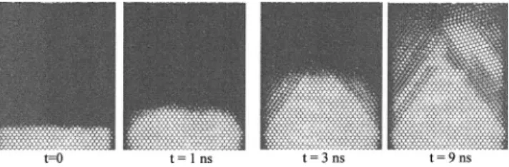
regrowth degrades the device performance.52,54In Fig.6 we illustrate the regrowth of a 14 nm thick fin structure oriented along具110典using MD calculations in a simulation cell con-taining 84 000 atoms. The amorphous phase is built by the accumulation of bond defects and Tersoff potential is used to describe the Si–Si interactions.7 The lateral sides contain 3
ML of a-Si, and lateral periodic boundary conditions are
used while the top and bottom sides are let free to allow for the volume change in a-Si. A crystalline seed is left at the bottom of the fin so that it can trigger SPER. The dynamics is followed by 9 ns at temperature just below melting ofa-Si.
Figure6shows that regrowth advances from the
amorphous-crystalline interface, starting from the middle of the fin, but it is halted at the vertical interfaces because of the stability of bond defects at interfaces. Then,兵111其planes start to form as the regrowth in this direction is slower than along具110典and 具100典directions,57preventing a clean regrowth. The detailed atomistic evolution provided by MD simulations demands long computational times. The capability to simulate SPER
shape evolution in continuum methods have been recently achieved using the level set approach, taking into account orientation dependence and curvature.58
IV. CONCLUSIONS
Process simulation capabilities must evolve to encompass processes, geometries, and materials considered for present and future devices. Detailed atomistic models are often too complicated or too slow to be used in actual process simula-tions but they are very useful to provide the physical under-standing for the development of simplified models computa-tionally more efficient. Ion implantation continues as the most promising technique to introduce dopants. Improved models have been developed to describe in detail dopant profiles, the kinetics of damage, and the interactions between dopants and defects. There is still a lot of room for improve-ment, specially related to the modeling of dopants in a-Si. Additional challenges arise in advanced architectures, such as FinFETs, because the introduction of highly tilted ions is quite inefficient and the regrowth ofa-regions in narrow de-vices is hampered by the slow regrowth at the free interfaces and兵111其planes. Although alternative materials, such as Ge or III-V compounds, are being considered for future tech-nologies, a vast effort needs to be made to catch up with the mature knowledge of the Si material properties, technology, and modeling.
ACKNOWLEDGMENTS
This work has been partially funded by the Spanish Gov-ernment under Project No. TEC2008-06069 and by Junta de Castilla y León under Project No. VA011A09.
1International Technology Roadmap for Semiconductors共www.itrs.net兲. 2M. S. Ameen, L. M. Rubin, M. A. Harris, and C. Huynh, J. Vac. Sci.
Technol. B 26, 373共2008兲.
3K. Mistryet al., Dig. Tech. Pap. - Symp. VLSI Technol. 2004, 50. 4R. Lindsayet al., Mater. Res. Soc. Symp. Proc. 765, D7.4共2003兲. 5N. Goelet al., Tech. Dig. - Int. Electron Devices Meet. 2008, 363. 6L. A. Marques, L. Pelaz, P. Lopez, M. Aboy, I. Santos, and J. Barbolla,
Mater. Sci. Eng., B 124–125, 72共2005兲.
7J. Tersoff, Phys. Rev. B39, 5566共1989兲.
8S. J. Cook and P. Clancy, Phys. Rev. B 47, 7686共1993兲.
9C. Krzeminski, Q. Brulin, V. Cuny, E. Lecat, E. Lampin, and F. Cleri, J.
Appl. Phys. 101, 123506共2007兲.
10K. L. Saengeret al., Mater. Res. Soc. Symp. Proc. 1070, 205共2008兲. 11M. D. Giles, J. Electrochem. Soc. 138, 1160共1991兲.
12G. Hobler, L. Pelaz, and C. S. Rafferty, J. Electrochem. Soc. 147, 3494
共2000兲.
13D. G. Ashworth, R. Oven, and B. Mundin, J. Phys. D: Appl. Phys. 23,
870共1990兲.
14G. M. Yu, P. B. Griffin, and J. D. Plummer, Tech. Dig. - Int. Electron
Devices Meet. 1998, 717.
15M. T. Robinson and I. M. Torrens, Phys. Rev. B 9, 5008共1974兲. 16J. F. Ziegler,The Stopping and Range of Ions in Solids共Pergamon, New
York, 1977兲, Vol. 1.
17M. Posselt and J. P. Biersack, Nucl. Instrum. Methods Phys. Res. B 64,
706共1992兲.
18G. Hobler, Nucl. Instrum. Methods Phys. Res. B 96, 155共1995兲. 19J. M. Hernandez-Mangas, J. Arias, L. Bailón, M. Jaraiz, and J. Barbolla,
J. Appl. Phys. 91, 658共2002兲.
20M. J. Caturla, T. Diaz de la Rubia, L. A. Marques, and G. H. Gilmer,
Phys. Rev. B 54, 16683共1996兲.
21P. Sigmund, Appl. Phys. Lett. 14, 114共1969兲.
22I. Santos, L. A. Marques, and L. Pelaz, Phys. Rev. B 74, 174115共2006兲. 23L. A. Marques, L. Pelaz, and I. Santos, Phys. Rev. B 74, 201201共2006兲. 24M. Posselt, Mater. Sci. Semicond. Process. 3, 317共2000兲.
25I. Santos, L. A. Marques, L. Pelaz, and P. Lopez, J. Appl. Phys. 105,
083530共2009兲.
26L. Pelaz, L. A. Marques, and J. Barbolla, J. Appl. Phys. 96, 5947共2004兲. 27G. Hobler and G. Otto, Mater. Sci. Semicond. Process. 6, 1共2003兲. 28J. A. van den Berg, S. Zhang, S. Whelan, D. G. Armour, R. D. Goldberg,
P. Bailey, and T. C. Q. Noakes, Nucl. Instrum. Methods Phys. Res. B 183, 154共2001兲.
29Y. Kunni, M. Tabe, and K. Kakiyama, J. Appl. Phys. 56, 279共1984兲. 30R. Duffy, M. J. H. van Dal, B. J. Pawlak, M. Kaiser, R. G. R. Weemaes,
B. Degroote, E. Lunnen, and E. Altamirano, Appl. Phys. Lett. 90, 241912
共2007兲.
31P. Pichler,Intrinsic Point Defects, Impurities and their Diffusion in
Sili-con共Springer, Wien, 2004兲.
32M. Aboy, L. Pelaz, L. A. Marques, P. Lopez, J. Barbolla, and R. Duffy, J.
Appl. Phys. 97, 103520共2005兲.
33K. Suzuki, Y. Kataoka, S. Nagayama, C. W. Magee, T. H. Buyuklimanli,
and T. Nagayama, IEEE Trans. Electron Devices 54, 262共2007兲.
34R. Duffyet al., Appl. Phys. Lett. 84, 4283共2004兲.
35V. C. Venezia, R. Duffy, L. Pelaz, M. J. P. Hopstaken, G. C. J. Maas, T.
Dao, Y. Tamminga, and P. Graat, Mater. Sci. Eng., B 124–125, 245
共2005兲.
36S. Mirabella, D. de Salvador, E. Bruno, E. Napolitani, E. F. Pecora, S.
Boninelli, and F. Priolo, Phys. Rev. Lett. 100, 155901共2008兲.
37A. Mattoni and L. Colombo, Phys. Rev. B 69, 045204共2004兲.
38S. H. Jain, P. B. Griffin, J. D. Plummer, S. Mccoy, J. Gelpey, T. Selinger,
and D. F. Downey, J. Appl. Phys. 96, 7357共2004兲.
39R. Duffy, V. C. Venezia, A. Heringa, M. J. P. Hopstaken, G. C. J. Maas,
T. Dao, Y. Tamminga, and F. Roozeboom, Mater. Res. Soc. Symp. Proc. 810, 437共2005兲.
40M. J. P. Hopstaken, Y. Tamminga, M. A. Verheijen, R. Duffy, V. C.
Venezia, and A. Heringa, Appl. Surf. Sci. 231–232, 688共2004兲.
41G. Impellizzeri, S. Mirabella, F. Priolo, E. Napolitani, and A. Carnera, J.
Appl. Phys. 99, 103510共2006兲.
42M. Diebel and S. T. Dunham, Phys. Rev. Lett. 93, 245901共2004兲. 43S. Boninelli, G. Impellizzeri, S. Mirabella, F. Priolo, E. Napolitani, N.
Cherkashin, and F. Cristiano, Appl. Phys. Lett. 93, 061906共2008兲.
44J. Kedzierski, M. Ieong, E. Novak, T. S. Kanarsky, Y. Zhang, D. Boyd, D.
Fried, and H.-S. Philip Wong, IEEE Trans. Electron Devices 50, 952
共2003兲.
45N. Collaertet al., Solid-State Electron. 52, 1291共2008兲.
46M. J. H. van Dalet al., Dig. Tech. Pap. - Symp. VLSI Technol. 2007,
110.
47V. Subramanianet al., Solid-State Electron. 51, 551共2007兲.
48H.-J. Gossmann, A. Agarwal, T. Parrill, L. M. Rubin, and J. M. Poate,
IEEE Trans. Nanotechnol. 2, 285共2003兲.
49S. Takeuchi, N. D. Nguyen, F. E. Leys, R. Loo, T. Conard, W.
Vandervorst, and M. Caymax, ECS Meeting Abstracts, 2008共 unpub-lished兲, Vol. 802, p. 2432.
50Y. Sasaki, K. Okashita, K. Nakamoto, T. Kitaoka, B. Mizuno, and M.
Ogura, Tech. Dig. - Int. Electron Devices Meet. 2008, 917.
51R. Duffy, G. Curatola, B. J. Pawlak, G. Doornbos, K. van der Tak, P.
Breimer, J. G. M. van Berkum, and F. Roozeboom, J. Vac. Sci. Technol. B 26, 402共2008兲.
52L. Pelazet al., Tech. Dig. - Int. Electron Devices Meet. 2008, 535. 53W. Vandervorstet al., Ion Implantation Technology Conference
Proceed-ings, 2008共unpublished兲, Vol. 1066, pp. 446–456.
54M. J. H. van Dal, R. Duffy, B. J. Pawlak, N. Collaert, M. Jurczak, and R.
J. P. Lander, Mater. Res. Soc. Symp. Proc. 1070, 67共2008兲.
55L. Pelaz, M. Aboy, P. Lopez, and L. A. Marques, J. Vac. Sci. Technol. B
24, 2432共2006兲.
56M. Aboy, L. Pelaz, L. A. Marques, L. Enriquez, and J. Barbolla, J. Appl.
Phys. 94, 1013共2003兲.
57L. Csepregi, E. F. Kennedy, J. W. Mayer, and T. W. Sigmon, J. Appl.
Phys. 49, 3906共1978兲.
58S. Morarka, N. G. Rudawski, and M. E. Law, J. Vac. Sci. Technol. B26,