The use of arc-erosion as a patterning technique for transparent conductive materials
J. Jiménez-Trillo
a,
A.L. Alvarez
b'*,
C. Coya
b,
E. Céspedes
c,
A. Espinosa
c a Dpt. Ingeniería de Circuitos y Sistemas, EUIT Telecomunicación, U. P. M, 2803I Madrid, Spain b Dpt. Tecnología Electrónica, Univ. Rey Juan Carlos, Móstoles, 28933 Madrid, Spainc Instituto de Ciencia de los Materiales (CSIC), Cantoblanco, 28049 Madrid, Spain
A B S T R A C T
Keywords: Arc Erosion
Cost-effective patterning ITO
Transparent conductive materials
Within the framework of cost-effective patterning processes a novel technique that saves photolithographic processing steps, easily scalable to wide area production, is proposed. It consists of a tip-probe, which is biased with respect to a conductive substrate and slides on it, keeping contact with the material. The sliding tip leaves an insulating path (which currently is as narrow as 30 um) across the material, which enables the drawing of tracks and pads electrically insulated from the surroundings. This ablation method, called arc-erosion, requires an experimental set up that had to be customized for this purpose and is described. Upon instrumental monitoring, a brief proposal of the physics below this process is also presented. As a result an optimal control of the patterning process has been acquired. The system has been used on different substrates, including indium tin oxide either on glass or on polyethylene terephtalate, as well as alloys like Au/Cr, and Al. The influence of conditions such as tip speed and applied voltage is discussed.
1. Introduction
In the past decade Organic Electronics has boosted the development of thin, transparent conductive oxide films, mainly of indium-tin oxide (ITO), either on rigid (glass) or flexible substrates. Currently Organic Electronics is facing the development of cost-effective manufacturing methods for mass production over large areas. Initiatives in this line have rendered attention to solution-processing techniques for the active organic layers [1,2] and to the use of flexible substrates. In this context, the process of creating electronic devices on a roll of flexible plastic, or roll-to-roll (R2R) technology, is considered the most promising solution for high-speed, large-area processing with great throughput. Jet-printing
[3,4], nano-imprint lithography (NIL) [5], and laser ablation [6,7] are currently the most used patterning techniques compatible with a R2R setup.
Despite the progress made, the search of low-cost procedures for patterning is still open. In 1999 Hohnholz et al. [8] observed that stripes of an ITO coated glass could be partially removed by sliding a hard metal tip onto the ITO, while applying a moderate voltage (-15 V) between both, tip and substrate. The complete removal of ITO was subsequently achieved by wet etching in a 2 M hydrochloric bath for a few seconds. This technique was proposed as a simple method for the subdivision of ITO on glass substrates[9]. It should be noticed that ITO may be a very
hard material [10] so that a simple mechanical scraping off is not suitable to electrically insulate two regions.
gas flux[12]. In this work we explain how is it possible to generate large discharges using continuous, low voltage sources.
In Section 2, the experimental set up to perform patterns on dif-ferent conductive materials is described. Experimental evidences that permit us to explain the physical mechanism and thus, to control the patterning process are explained in Section 3. Conclusions are sum-marized in Section 4.
2. Experimental setup
A computer-assisted system (Fig. 1) consisting of an assembly of three micropositioners along the XYZ axis, has been developed. Motion along each axis is carried out by a high precision PLS-85 MICOS linear stage, provided with a 2-phase stepper motor and a closed loop system that improves accuracy. Resolution and repeatability down to 1 um are guaranteed. The XYZ micropositioner is driven by a SMC-corvus-eco MICOS controller, connected to PC via RS-232 or USB interface, which is programmed with a specific software. Thus, the motion may follow a previously designed pattern. The maximum scanning speed allowed by our specific controller is 15 mm/s, and the working area comprises 10x10 cm2.
A home-made mechanical head has been designed and adapted to the micropositioner. It is mounted on a methacrylate support to ensure its electrical insulation with the machine body. This piece includes a spring probe (marked by the yellow arrow in the picture) that enables upward and downward motions of the steel (or tungsten) needle, so different degrees of pressure may be exerted in contact with the sample. The probe metal type is not apparently a critical issue but since it works in contact mode, a hard metal is recommended when working with robust materials like ITO. Thus, the equipment behaves as a plotter, i.e., the pattern is designed with a vector-graphic design software, the resulting file is translated by the electronic controller, and the pattern is engraved on the sample.
The conducting tip is connected to a usual continuous power supply (2 x 30 V, 3 A) which constitutes a difference with respect to the pulsed voltage used in industrial electro-discharge machining. A home made circuit is connected in series to the needle with two purposes: on one hand, to bypass the internal 220 uF capacitor of the power supply substituting it by the desired external capacitors, and on the other hand, to ensure a fast charge and recharge of them.
Fig. 1. Experimental set up for arc erosion patterning by means of a computer assisted XYZ micro-positioner. Yellow arrow marks the probe tip.
The voltages at the tip and at the external capacitor are monitored by a 200 MHz band-width oscilloscope during operation. Profiles of the performed grooves were measured using an Alpha-Step IQcontact profilometer by Tencor Instruments.
3. Results and discussion
When the tip comes into contact with the ITO substrate at a bias V = 0, the voltage may then be gradually increased up to tens of volts without creating any local damage, despite the high current (amps) injected into the material. In these conditions the tip slides without affecting the surface. However, if the tip is biased away from the surface at a suitable voltage of, e.g., 12 V, and then it approaches the ITO surface, a spark is generated at a sufficiently short distance, creating an insulated region around the tip and hence an open circuit. Despite the power supply is protected against short-circuits with a current limitation stage, the source includes an output bypass capacitor (around 220 uF) to filter high frequency signals. This capacitor is able to discharge at a very high current rate because it is directly connected to the low contact resistance.
Starting from this initial condition, the tip leaves a brown colored, insulated path as it slides onto the ITO surface. If the line depicts a closed loop, the inner region is insulated from the outer one by R>2 Mohm. After a subsequent wet etching the residual ITO is removed achieving an open circuit between both regions.
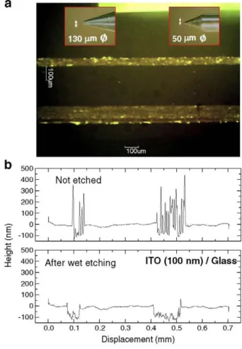
In Fig. 2a, a plane view of the traces left on ITO by two different probes is shown. Both were performed under identical conditions, at a working voltage of 12 V. The inset in Fig. 2a shows the probe tips,
having diameters of 50 urn and 130 urn, very similar to the resulted stripe widths. From these results it is obvious that discharges pro-duced by wider tips should involve a larger energetic supply. This means that wider tips may require a higher output capacitor in order to provide this energy, otherwise erosion may fail.
In Fig. 2b, the profiles of both grooves, as measured by contact profilometry, are plotted. The upper profile shows the sample just as eroded and the lower one the sample after wet etching. Before etching, although the eroded zone shows a partial insulating character (a few Mohms), the ITO is not removed but cracked. This is confirmed by profilometry, which reveals protruding material up to several hundred nm from the surface (upper profile). The lower profile shows grooves after treated with 6 M hydrochloric acid at room temperature for 10 s. According to Ref. [13] not very relevant etching of the ITO layer (few A/s) is expected at this concentration of hydrochloric acid. We did not measure significant changes in resistivity (ohm/square) on test samples. However, the previously cracked zones are easily removed. This may be partially attributed to the higher area exhibited by the cracked material. This is an interesting result because it indi-cates a selective etching without using photoresist protection.
The voltage between tip and material, i.e. at the output bypass capacitor, has been monitored in the oscilloscope during tip motion on an Au(80nm)/Cr (5nm)/glass sample. A sequence of electrical discharges, separated by intervals of no conductance, is typically observed, as displayed in Fig. 3. The applied voltage was 10 V, and the sharp voltage falls indicate discharges. Notice that the voltage recovering (recharge) is very fast. An expansion of the time scale revealed it takes less than 1 us. The slowing down observed when the raising voltage is slightly below 10 V is an artifact due to the time response of an internal diode, which is not relevant for the procedure. Notice that in this case, the tip speed was fixed to 1 mm/s for an easier handling of the oscilloscope screen captures. The observations are interpreted as follows:
The energy stored previously to the discharge is expressed as
C -V (1)
where V is the external bias and Ceq is the equivalent output capacitance. Ed is delivered in the short time interval of the discharge, in the range <1 us. It means a power of several watts concentrated in a small region around the tip. This causes a sublimation of the material in this region which then becomes electrically insulated, because the heat dissipation rate of the material is not enough for removal of the excess energy. As
~
r>
V
n\/-50(
V A T
-V/div
>r
, ll.,l) f.is/div
rrr
'trTfJ
'
¡1
-~%~y
the tip travels towards the boundary of this region, there is no conductance and then, the capacitance is recharged. When the tip reaches the close conductive region, the capacitance generates a new discharge, and so on. If there is no insulation or if the tip reaches the conductive boundary too soon (due to a high speed motion) the capacitor is not fully recharged and the erosion eventually fails.
In consequence, the physical limit for the scanning speed is deter-mined by two factors: i) the time to recharge the capacitor in order to assist the next discharge, and ii) the diameter of the eroded area around the tip. It means that the capacitor should recharge before the tip arrives to the closest conductive region, so a new spark may be produced. In our case, the circuitry may recharge this capacitor very fast (see Fig. 3), in around 1 us. Concerning the diameter of the eroded region around the tip, it depends on the applied voltage, but for the typical voltages used on ITO, 8-20 V, it can range from one to tens of um. That means scanning speeds higher than hundreds of mm/s can be used.
These results indicate that to achieve precision all machining char-acteristics, such as operating voltage, output capacitance, as well as tip speed have to be adjusted optimally.
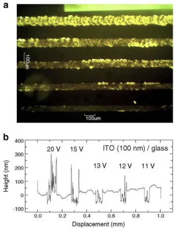
Fig. 4 shows stripes eroded at different operating voltages, 11 V, 12 V, 13 V, 15 Vand 20 V (from bottom to top), using 50 urn diameter tip. A stripe widening from 50 um to 100 um is observed with in-creasing voltage. However, this widening means a loss of patterning quality in terms of waviness. The widest stripe (top one) seems to be made of overlapping circular crowns which presumably correspond to each discharge. This means that at 20 V, the region eroded by one discharge extends 20-30 urn beyond the tip. Picture of Fig. 4a was taken after wet etching. The contrast observed between stripes is an indication of the etching efficacy. Thus, stripes performed at lower voltages (11 V, 12 V), with poor contrast, were reasonably etched, as confirmed in Fig. 4b. In contrast, the etching did not work well in
a
"* 400
300
I 200
.g> ioo
CD
X 0
-100
20 V 15 V ITO (100 nm)/glass
13V 12V 11V
o.o 0.2 0.4 0.6 0.8
Displacement (mm)
Fig. 3. Monitored voltage at the tip during motion. The falls' mean discharge processes. Tip speed was 1 mm/s, so a time division is equivalent to a 500 nm path.
Fig. 5. Grooves performed by arc erosion on a Au/Cr film on PET using a tip 40 |im diameter. Different widths between 40 and 200 |jm were obtained by changing the continuous operating voltage.
those stripes performed at higher voltages (15 V, 20 V). This is an indication that by changing operating voltage not only size changes but different qualities of eroded material are obtained.
Working on ITO at a typical 12 V operating voltage, we have not observed changes in the groove quality for the range of scanning speeds <15 mm/s allowed by the system. But as the operating voltage was reduced below 10 V, an increasing of fails (interruptions oferosion) was observed at high scanning speeds.
Al(120nm)
Polym. (70 nm)
ITO
(130 nm)
Regarding the output capacitance, the capacitor used is above a certain value around 1 uF to be able of supplying enough charge to break the material. Then, no enhancement of the erosion is observed for higher capacitances. However, as reducing the capacitance below 330 nF, the frequency of fails gradually increases.
In Fig. 5 different grooves on Au (80 nm)/Cr film on PET have been performed with the same tip, 40 um diameter, just varying the operating voltage around 10 V. No wet etching was necessary in this case. In general, lower operating voltages (2-4 V) are required to pattern aluminum layers, mainly due to its lower specific heat, but also to a possible lower adhesion to the substrate. Actually it is possible to make a selective etching when the operating voltage to remove the upper conductive layer is lower than that needed to remove the lower one. To illustrate this effect we have performed patterns on Al (at a working voltage of 3 V) deposited on top of ITO, without causing any damage on it. For that purpose we have used commercial ITO (130 nm)/glass substrates, previously patterned by photolithography, on top of which an Al(120 nm)/polymer(70 nm) bilayer was deposited (by Joule evaporation and spin coating respectively). Fig. 6 provides a cross section of the layer structure obtained after removing aluminum in a wide extension of 650 um.
a
glass
Arc-erosion
J}
6 5 0 (j.m
0.4 0.6 0.Í
Displacement (mm)
Fig. 6. Patterning of an Al(120 nm)/Polymer(70 nm) bilayer deposited on top of a step of ITO (130 nm thick) on glass, (a) sketches the layer structure before and after Al erosion, (b) shows a cross section recorded by contact profllometry.
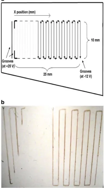
It should be noticed that in all cases the tip was negative polarized with respect to the material. When the polarity is inverted and the tip is positively polarized, a significant erosion of the tip is observed during operation, which eventually causes an open circuit and the interruption of the process. This can be seen in Fig. 7, where a tip biased at + 25 V just patterns a short ITO segment before interrupting, whereas the tip polarized at —12 V keeps working properly for long distances. This result also supports the assumption that a discharge or a plasma assisted sputtering is driving the physical process of the erosion.
Using this setup, we have been able to control the electro-discharge process, and hence to draw features onto a variety of material sub-strates with different resolutions and qualities, as displayed in Fig. 4 for Au/Cr/PET, or ITO/glass, ITO/PET, Au/PET, AI/PET, and Al/glass. Al-though this technique is limited to conducting or semiconducting materials, this is not a great limitation for organic devices, where the device architecture is mainly determined by the electrode patterning, and etching the organic layers is less usual.
4. Conclusions
In conclusion, the search of new experimental evidences from voltage monitoring in the time domain and profilometry, has allowed us to explain the physical processes behind the patterning of con-ductive materials performed by means of a continuous, low voltage-biased tip. This also allowed optimizing the control over this tech-nique in order to improve resolution and quality of the patterned lines. Even though this technology is still under development, this
work shows very promising results that can be easily scaled to a large area line production in a cost-effective way.
Acknowledgments
Financial support by Comunidad Autónoma de Madrid under project S2009/MAT-1756 and S2009/ESP-1781 and by Ministerio de Educación y Ciencia (Spain) under MAT2009-08786 and TEC2009-13991-C02-02 projects, is gratefully acknowledged.
References
[1 ] A.R. Duggal, CM. Heller, J.J. Shiang, J. Liu, LN. Lewis, J. Display Technol. 3 (2007) 184.
[2] Y. Ohmori, H. Kajii, Y. Hiño, J. Display Technol. 3 (2007) 238.
[3] M. Singh, H.M. Haverinen, P. Dhagat, G.E. Jabbour, Adv. Mater. (Weinheim, Ger.) 22 (2010) 673.
[4] M. Bale, J.C. Carter, C.J. Creighton, H.J. Gregory, P.H. Lyon, P. Ng, L Webb, A Wehrum, J. Soc. Inf. Display 14 (2006) 453.
[5] S.H. Ann, LJ. Guo, Adv. Mater. (Weinheim, Ger.) 20 (2008) 2044.
[6] Y.H. Tak, C.N. Kim, M.S. Kim, K.B. Kim, M.H. Lee, S.T. Kim, Synth. Met. 138 (2003) 497.
[7] L.C. Zhu, G.X. Liu, D. Ming, Optoelectron. Lett. 2 (2006) 426.
[8] D. Hohnholz, K.H. Schweikart, M. Hanack, Adv. Mater. (Weinheim, Ger.) 11 (1999) 646.
[9] D. Hohnholz, K.H. Schweikart, M. Hanack, Synth. Met. I l l (112) (2000) 385. [10] S. Suzuki, N. Hashimoto, T. Oyama, K. Suzuki, J. Adhes. Sci. Technol. 8 (1994) 261. [11] S. Kumar, R. Singh, T.P. Singh, B.L Sethi, J. Mater. Process. Technol. 209 (2009)
3675.
[12] F.N. Leao, I.R. Pashby, J. Mater. Process. Technol. 149 (2004) 341.
[13] Shabbir A Bashar, Ph.D. Thesis, King's College London, University of London, U. K.,