A Comparison of Approaches for High-level Power Estimation of LUT-based
DSP Components
Ruzica Jevtic and Carlos Carreras
Dpto. de Ingenier´ıa Electr´onica
Universidad Polit´ecnica de Madrid
Ciudad Universitaria s/n, 28040 Madrid, Spain
email:
{
ruzica, carreras
}
@die.upm.es
Domenik Helms
OFFIS Research Institute
D-26121 Oldenburg, Germany
email: [email protected]
Abstract
We compare two approaches for high-level power esti-mation of DSP components implemented in FPGAs for dif-ferent sets of data streams from real-world applications. The first model is a power macro-model based on the Ham-ming distance of input signals. The second model is an an-alytical high-level power model based on switching activity computation and knowledge about the component’s internal structure, which has been improved to also consider addi-tional information on the signal distribution of two consec-utive input vectors. The results show that the accuracy of both models is, in most cases, within 10% of the low-level power estimates given by the tool XPower when cycle-by-cycle input signal distributions are taken into account, and that the difference between the model accuracies depends significantly on the nature of the signals. Additionally, the effort required for the characterization and construction of the models for different component structures is discussed in detail.
1. Introduction
Due to their low cost and ability for reconfiguration, FP-GAs have become an ideal solution for various embedded designs. However, as FPGAs use a large number of logic and routing resources, it is necesarry to use power opti-mization techniques during a design flow to avoid exces-sive power consumption. Power optimization techniques at lower levels of abstraction need transistor or gate level cir-cuit descriptions, leading to severe penalties in design time. The design should be optimized at the earliest possible time, resulting in the algorithm and architecture design phases as the preferred choices for power optimization.
High-level design modifications also call for high-level power estimation. The most common estimation approach
is called Power Macromodelling [1, 2, 5, 6, 11, 12], where the power model is expressed as an equation with variable parameters depending on the input and output signal statis-tics, and the input word-lengths. The design is simulated at the transistor or gate level for many different signal statis-tics and combinations of input word-lengths, and the co-efficients standing by the variables are obtained through a multivariable regression over power values gathered from these simulations. The resulting function is often a third order polynom which contains a large number of unknown coefficients, and thus, numerous low-level simulations are needed. For the parameter values different from those used for the characterization, a solution is sought in numerical methods. The accuracy of these power models can be sig-nificantly increased by considering signal statistics between each two consecutive input vectors instead of considering the average value over the whole input data set. This is one of the main features of the Hamming distance power model (Hd-model) [2, 6, 11], and it is also a feature of the analyti-cal model considered here, as it is explained later.
Another approach used for high-level power estimation is based on the analytical computation of the switching ac-tivity of the component and on the implementation details of the components structure [3, 4]. The models are precise and parameterizable in terms of input word-lengths and in-put signal statistics and require a smaller number of low-level simulations. The drawback of this approach is that it has to be adapted to every different component’s structure.
Therefore, it is important to evaluate these high-level power estimation techniques regarding their accuracy and time needed for their characterization and execution, as to find the most suitable approach for a given application.
real-world applications, we compare this enhanced analytical model and the Hd-model. This allows us to identify the type of applications where one model achieves higher accuracy than the other, so we can specify different sets of real-world scenarios suitable for each of the compared models. Finally, we evaluate other aspects related to the practical application of the approaches.
The paper is organized as follows. Section 2 highlights the previous work on high-level power estimation. Section 3 gives a brief overview of the Hd-model. Section 4 presents an analytical power model. Section 5 describes an input vector classification, made in order to further improve the accuracy of the analytical model. Experimental results are given in Section 6, followed by conclusions in Section 7.
2. Related work
High-level estimation models can be divided into three groups according to the characterization of the input data set. The first one, considersnchosen bit-level signal statis-tics that are introduced as variables into a power equation. Coefficients standing by the variables are found through ex-tensive simulations, which are listed into an n-dimension ar-ray in look-up table models ([1, 12]). The number of these simulations is reduced in equation-based macro-models [5], but is still quite high, as for some components the number of coefficients that needs to be calibrated goes up to 20.
The second power estimation group is based on power macro-models constructed by using the spatio-temporal correlations previously defined as Hamming distance [2, 6, 11]. This methodology tends to give large errors when two different input signals that result in different output statis-tics, are characterized with the same signal parameters [8].
The third power estimation group considers word-level signal statistics such as variance, mean and autocorrelation coefficient. In [9], a signal word is divided into three re-gions according to its word-level signal statistics: LSB un-correlated bits, un-correlated bits in the linear region, and MSB sign bits. A black-box model of the capacitance switched in each activity region of the module is obtained through extensive simulations. The power models in [4] estimate logic power of DSP components implemented in FPGAs in the presence of glitching and correlation. The number of circuit simulations needed for characterizing the power model is highly reduced with respect to other power esti-mation methods. The main drawback of these approaches is the need to adapt the analytical computation method to every different component structure.
3. Hamming distance Power Model
Hamming distance models represent ’black box models’, that do not use any knowledge of the components internal
structure, but instead, abstract to input data statistics. The variables used in Hd-models are Hamming distance, Signal distance and Zero distance. The Hamming distance is defined as the number of transitions between two consec-utive input vectors:
Hd=t0→1+t1→0
i,jti→j
(1)
whereti→jis the number of bit transitions from i to j within two consecutive input bit-vectors.
The Signal distance is the number of input bits that are fixed to logic one in two consecutive input vectors.
Sd=t1→1
i,jti→j
(2)
This number increases the probability that the switching ac-tivity of the inputs is propagated through the component [2]. The Zero distance is the number of input bits that are fixed to logic zero in two consecutive input vectors and is obtained from the following equation:
Hd+Sd+Zd= 1 (3)
These three variables are used to classify different in-put streams. Normally, the characterization set includes every possible combination of input-streams for Hd =
{0,0.25,0.5,0.75,1}andSd={0,0.25,0.5,0.75,1}. The combinations are limited by (3) and for a component with inputs A and B, the number of possible sets ofHdA,HdB,
SdAandSdBis:
M = (1 + 2 +...+nA)∗(1 + 2 +...+nB) (4)
wherenAandnB are the number of different values in the setsHdAandHdBrespectively.
The components’ input word-lengths or/and their com-bination, are chosen as the last model variables in order to make the model scalable. In this case, the characterization process has to be repeated for every component with the input sizes taken from the input word-length setbw.
Without a significant sacrifice of the accuracy of the model, the Hd-model can be expressed as a product of two separate functions: one is expressing the dependency on the input word-lengths and the other the dependency on the nor-malizedHdandSdvalues [7].
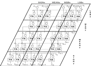
Figure 1. Regional decomposition of an array multiplier.
4. Analytical High-level Power Model
In [4], a high-level power estimation model for DSP components implemented in FPGAs is presented. This model has been further improved in [3] by considering both zero-mean and non-zero mean signals. Next, a brief overview of the approach is given.
Power consumption of a module can be represented as
P =a·SW (5)
where SW is the total switching activity produced inside the component and constant a represents the product of three power terms: squared power supply, which is constant for a specific FPGA architecture, clock frequency, which is fixed for a specific design, and load capacitance,Cl, which is assumed to be constant in a case of DSP modules imple-mented in FPGAs. Although, the carry wires have a lower capacitance than sum wires as they are directly connected to the next adder cell via dedicated routing, the assumption made for Cl can be considered valid for the purposes of high-level estimation. Arithmetic components exhibit a reg-ular, repetitive structure composed of full-adder cells, and thus,Clcan be regarded as an effective capacitance when both types of wires are accounted for. The constant a is obtained with one-time low-level power measurement for some chosen component size and input signal statistics, and from the computation of the corresponding total switching activity of the component for the chosen parameters.
The total switching activity is obtained as the sum of the switching activities of the outputs and carry bits of all the full-adder cells in the component. The switching activity computation starts from the switching activities of the input bits. The basic approach is to divide the input words into ac-tivity regions according to signal-word statistics similar to
those in [9]. In the case of non-zero mean signals there are four regions: the LSB region with switching activity of 0.5 as its bits behave as uncorrelated bits, the linear region with correlated bits [9], a mean region composed of the mean bits that remain fixed in all signal words, and a sign region com-posed of all ’0’s or ’1’s, depending on the sign of the mean. The linear region is further approximated by attributing the bottom half of its bits to the LSB region while the upper half of its bits are grouped in a so-called MSB region with con-stant switching activity [9]. The switching activity of each of the input bits is calculated according to [10]:
ti = 2·pi·(1−pi)·(1−ρi) (6)
wherepiis the bit probability, andρi is the bit-level auto-correlation coefficient which can be approximated byρfor the MSB bits, it has a value 0 for the LSB bits, and a value 1 for the mean and sign bits. Based on the signal-word re-gional decompositon, a whole component can be divided into activity regions as shown in Fig. 1 for an array multi-plier. With known values of the switching activities of the input bits and the probabilities of these bits being ’0’ or ’1’, an analytical method is employed to calculate the switching activity on the outputs of all full-adder cells [4].
Once the constant a is computed, the formula can be used for power estimation of any other component size and signal statistics. In order to obtain a power estimate, it is only neccesary to re-compute analytically the total switch-ing activity for the new input parameters.
The model has been further extended in order to consider glitching produced inside the component [3]. Although how glitches propagate through logic depends on the logic func-tion they pass through, once again, the fact that the DSP components can be built by repeating one elementary logic block (together with its connections to the neighbouring cells) throughout an array, allows us to make the following assumption. As the repeated cell always has the same logic function, and practically the same delay of the input signals, the difference in glitching at the outputs of two logic blocks will depend on the difference in the transition activities of their inputs. Thus, it is considered that the most significant amount of glitching produced inside the component is gen-erated at the most active regions of its inputs. The signals considered here have non-zero mean Gaussian distribution and thus, the multiplier can be divided into 16 different ac-tivity regions. The mean and sign bits have a fixed value and, therefore, zero activity. Hence, the glitching model represents the sum of the glitching produced in the remain-ing four component’s regions: LSBx-LSBy, LSBx-MSBy, MSBx-LSBy and MSBx-MSBy in Fig. 1.
glitch-ing produced in the MSB and LSB region, as the amount of glitching is assumed to be proportional to the transition activity of the input bits. As each basic element has two different inputs, this relationship is represented as the prod-uct of two such coefficients:l1andl2. The total amount of glitching in each of the regions is obtained as a sum of the average glitching at the output of a LUT, over all LUTs in the region.
The final model for estimating the power consumption in the presence of glitching and autocorrelation is given as:
P =b·(SW+k·G) (7)
wherekis an empirically derived constant which represents the average glitching at the output of one LUT in the LSBx-LSBy part of the component andb represents the product of the three power terms, equivalent to the constant a in (5). G represents the sum of the total number of LUTs in each region, properly scaled by the coefficientsl1 andl2. Two low-level power measurements for different multiplier sizes using the sameρare sufficient in order to determine coefficientsbandk. In order to increase the accuracy of the model, we use a multivariable regression with more than two measurements for obtaining these two coefficients. The number of measurements is still significantly smaller than in any other high-level approach using power macro-modules.
5. Cycle-by-cycle accuracy
In [6], it was demonstrated that using the Hamming dis-tance distribution, rather than average values, increases the estimation accuracy when power has a non-linear depen-dency onHd. This is precisely the case in many DSP data-streams and data modules.
The Hamming distance distribution is obtained in the following way. For each two consecutive input vectors of both operands A and B, the Hamming and Signal distances are calculated. Hence, the number of appearances for each combination ofHdA,SdA,HdB andSdBis available for a given data set. The products of the probabilities and the corresponding power values are added to form a new and more accurate power estimate.
We have included the same methodology as a part of the analytical model, but instead of computingHdandSd, we have classified each two consecutive input vectors as be-longing to different Gaussian distributions, depending on the number and the value of the MSB bits that are the same in both vectors. Consider the following three vectors:
010010110 010011010
010110100 (8)
We say that the first two belong to the Gaussian distribu-tion with the most significant mean bits equal to 01001, and
the second and the third belong to the Gaussian distribution with the most significant mean bits equal to 010. In both cases, the first bit that stands immediately after the mean bits, changes with a switching activity of 1, and the rest of the bits behave as uncorrelated, random bits with a switch-ing activity of 0.5. Based on this classification, we have applied the power model described in Section 4, to each Gaussian distribution detected in the input data set and the corresponding power value was summed to the expression for the final power estimate, according to the number of in-put vectors associated to it:
P=
i
Pi· ni
N−1 (9)
whereN is the total number of vectors in the input data set,
ni is the corresponding number of vector pairs belonging to theith Gaussian distribution, andPiis its corresponding power value computed as in (7).
6. Experimental results
The experiments have been designed in order to present the comparison of the analytical power model and the Hd-model for signals taken from real-world applications. They have been applied to multipliers and adders implemented as Xilinx IP Cores in Virtex II devices. All the estimated values have been compared to low level power estimated values obtained from the Xilinx tool XPower [13].
We have used 16x16 and 32x32 components and signals with zero-mean gaussian distributions and autocorrelation coefficients of 0, 0.9, -0.9 and -0.99 as the characteriza-tion set for the construccharacteriza-tion of the analytical power model. A typical characterization set mentioned in Section 3, has been used for Hd-model construction.
The experiments have been carried out for five different types of input stimuli. The pattern set includes:
1) row speech signal 2) image signal
3) memory access index (counter-like signal)
4) randomly chosen signal variable in a C-code FDCT 5) uniform white noise
Each of the power models has been used in two different ways in order to obtain the estimation errors for the given input data. The first one takes average values of the signal statistics for the whole input data set (marked as Average in Tables 1, 2 and 3), while the second one considers cycle-by-cycle input signal characteristics (marked as Cycle).
Table 1. Comparison of two models for multi-pliers.
Data Hd-model error [%] Analyt. model error [%] types Average Cycle Average Cycle
I 7.41 4.25 12.65 -8.8
II 2.97 -3.96 -10.03 -10.23
III 43.75 35.33 47.71 -11.87
IV 11.07 0.63 31.03 33.1
V -5.25 -8.23 -10 -0.29
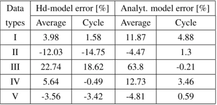
Table 2. Comparison of two models for adders
Data Hd-model error [%] Analyt. model error [%]
types Average Cycle Average Cycle
I 3.98 1.58 11.87 4.88
II -12.03 -14.75 -4.47 1.3
III 22.74 18.62 63.8 -0.21
IV 5.64 -0.49 12.73 3.46
V -3.56 -3.42 -4.81 0.59
normally composed of ’1’s and ’0’s randomly distributed in a signal-word with the bits that are switching also located at randomly distributed bit-positions. On the other hand, a counter-like signal has established bit positions of ’1’s and ’0’s and the bits that are switching are determined. Thus, applying the cycle-by-cycle power computation, barely im-proves the accuracy of the model.
The analytical model with cycle-by-cycle computation gives good results for all signals except in multipliers for types IV. We have observed that this is entirely due to the nature of the signals in the FDCT. As the bit switching activ-ity is distributed over the bit-positions in a random fashion, signal-word decomposition explained in Section 4, can not be performed in this case. This is the reason for equally poor performance when considering average distribution for the data set, as well as cycle-by-cycle signal distribution. It can be also noted that cycle-by-cycle computation improves the accuracy of the analytical model up to 60% for type III.
In the continuation, we extend the comparative analysis of the two high-level power estimation models with four additional aspects that try to establish the applicability of the approaches in real world situations.
The first aspect is the computational effort used for the model characterization and utilization. The number of sim-ulations needed for the Hd-model construction was 225
(ac-Table 3. Comparison of two models for com-ponent size different from input signal bit-width
Data Hd-model error [%] Analyt. model error [%] types Average Cycle Average Cycle
Mul.-II 56.73 55.18 3.24 -13.67
Mul.-III 41.83 33.94 47 -12.58
Add.-II 10.5 9.36 -4.44 1.33
Add.-III 36.88 34.2 63.9 -0.15
cording to (4)) for each component with specified operand sizes, while only 8 simulations were needed for the con-struction of the analytical model that can be then used for component of any operand sizes. It can be seen that the Hd-model is extremely dependent on the accuracy and time performance of the low-level simulation tool as it requires a large number of low-level simulations. The best accuracy is achieved when the model is characterized with on-board power measurements. FPGA power measurements need to be carefully prepared and processed in order to obtain sep-arate interconnect and logic power values, thus, making the automatization of the measurement process extremely dif-ficult. In the case of the analytical model, the number of simulations needed for model characterization is highly re-duced. Hence, it can be directly based on power measure-ments leading to a better accuracy.
There is also a difference in the computational effort re-quired by each model when cycle-by-cycle signal statistics are taken into account. In the Hd-model, for each pair of consecutive vectors, the parameters Hd and Sd have to be computed, meaning that the computation includes all the bits in each signal-word. In the analytical model, this num-ber is reduced to the numnum-ber of the most-significant bits that have the same value in both vectors. However, when equa-tion (9) is applied, the values ofPi are taken directly from the table or interpolated from the neighbouring table values in the case of Hd-model, while they need to be computed for the analytical model. When these two effects are both taken into account, the Hd-model has some advantage over the analytical model, although the difference is barely evi-dent as each estimatePionly takes a few miliseconds in the worst case.
the analytical approach shows a 4.77% mean relative er-ror for the cycle-by-cycle and a 20% erer-ror for the average model excluding data type IV.
The results in Tables 1 and 2 are given for components where the size of the input operand was adjusted to the input signal-word size. However, when resources are shared, it is often the case that smaller word-length input signals enter larger word-length component inputs. Thus, the third aspect is the model accuracy when resource sharing is considered. In this case, there will be no difference in the power estimate value from the analytical model, as the parts of the compo-nent that are not exhibiting any switching activity will not contribute to the total power. The Hd-model will also ac-count for this difference through the Hd andSd as they will decrease with respect to the full input length. However, the Hd-model is characterized assuming that the bits that are switching are located at randomly distributed bit positions, but in this case, the bits that are switching are all located at the LSB positions in the signal word. Hence, the Hd-model will tend to overestimate the power consumption. Table 3 shows the errors for the Hd-model and the analytical model when 8-bit signals of data type II and 13-bit signals of data type III are used as inputs of 16x16 multipliers and 16x16 adders. It can be seen that the Hd-model error in most cases increases significantly with respect to the values in Tables 1 and 2, while the analytical model maintains its accuracy.
The final aspect is the model construction for different component structures. The models used for the comparison presented here had the internal architecture of a row-adder tree multiplier and a carry-skip adder, as these structures are used for the implementation of cores in Xilinx FPGAs. The Hd-model methodology does not depend on the com-ponent structure, and as such can be easily adjusted to any given component. On the other hand, the component struc-ture is an important information for the switching activity computation in the analytical model. Thus, each time some component is replaced with the module of the same func-tionality, but different structure, the analytical computation method has to be specially adapted to the new features of the component internal architecture.
7. Conclusion
We have presented a comparison between two high-level power estimation models: the Hamming distance model and the analytical model, considering both average values of in-put data set statistics and cycle-by-cycle accuracy. Addi-tionally, the analytical power model has been improved to consider signal statistics between each two consecutive in-put vectors, which is a methodology inspired by the Ham-ming distance model. The experiments were performed on real-data applications and the results show that the accuracy of the analytical model is improved up to 60% when
cycle-by-cycle signal statistics are taken into account.
When comparing the two models, analytical model achieves better accuracy when considering highly-correlated signals, while the Hd-model gives better results when the switching activity of the input bits is distributed in a random fashion over the bit positions. Also, in practice, the analytical model needs significantly smaller number of low-level simulations for its characterization than the Hd-model, and achieves better accuracy when resource sharing is used. Still, when the operand word-length is ad-justed to the input word-length, for most of the applications the Hd-model is slightly more accurate than the analytical model, and it does not require any changes in its model characterization method for different component structures.
Acknowledgements: This work was supported in part by the Spanish Ministry of Education and Science under project TEC2006-13067-C03-03.
References
[1] S. Gupta and F. N. Najm. Power modeling for high level power estimation. IEEE Trans. On VLSI Systems, 8:18–29, February 2000.
[2] D. Helms, E. Schmidt, A. Schulz, A. Stammermann, and W. Nebel. An improved power macro-model for arithmetic datapath components. PATMOS’02, pages 16–24, Septem-ber 2002.
[3] R. Jevtic and C. Carreras. Analytical high-level power model for lut-based components.PATMOS’08, September 2008. [4] R. Jevtic, C. Carreras, and G. Caffarena. Switching activity
models for power estimation in fpga multipliers. ARC’07, LNCS (Springer), 4419:201–213, March 2007.
[5] T. Jiang, X. Tang, and P. Banerjee. Macro-models for high level area and power estimation on fpgas. Proc. on GLSVLSI’04, pages 26–28, April 2004.
[6] G. Jochens, L. Kruse, E. Schmidt, and W. Nebel. A new pa-rameterizable power macro-model for datapath components.
Proc. on DATE ’99, pages 29–36, March 1999.
[7] G. Jochens, L. Kruse, E. Schmidt, and W. Nebel. Power macromodelling for firm macros. Proceedings of the PAT-MOS’00, pages 24–35, September 2000.
[8] F. Klein, G. Araujo, R. Azevedo, R. Leao, and L. dos San-tos. On the limitations of power macromodeling techniques.
ISVLSI ’07, pages 395–400, May 2007.
[9] P. Landman and J. Rabaey. Architectural power analysis: The dual bit type method. IEEE Trans. On VLSI Systems, 3(2):173–187, June 1995.
[10] S. Ramprasad, N. R. Shanbhag, and I. N. Hajj. Analyti-cal estimation of signal transition activity from word-level statistics.IEEE Trans. on CAD, 16(7):718–733, July 1997. [11] A. Reimer, A. Schulz, and W. Nebel. Modelling
macromod-ules for high-level dynamic power estimation of fpga-based digital designs.ISLPED ’06, pages 151–154, Oct. 2006. [12] L. Shang and N. K. Jha. High-level power modeling of cplds