Effect of alkali doping on CIGS photovoltaic ceramic tiles
21
0
0
Texto completo
(2) efficiency relative to the standard (STD) solar cell sample chosen for comparative purposes. Keywords: CIGS solar cell; ceramic enamel; sodium; potassium.
(3) 1. Introduction Thin film technology have several potential advantages to Si for PV applications, such as better light absorption (10-110 times more efficient), allowing the use of very thin absorbers (ranging from 1.5 to 3 µm in contrast to hundred microns for Si) and thus less materials use for the fabrication of solar cells (El Chaar, et al. 2011; Park, et al. 2012; Todorov, et al. 2006; Todorov, et al. 2013; Jung, et al. 2010; Contreras, et al. 2006; Reinhard, et al. 2013). They can easily be integrated on several kinds of substrates as soda-lime glass (Zhang, et al. 2014; Furue, et al. 2013; Park, et al. 2011), light weight polymers (Reinhard, et al. 2015; Chirilă, et al. 2011; Caballero, et al. 2011), stainless steel (Pianezzi, et al. 2012; Liang, et al. 2016; Wuerz, et al. 2012) and ceramics (Fraga, et al. 2016; Calvet, et al. 2015; Fraga, et al. 2015; Calvet, et al. 2015). The Cu(In,Ga)(S,Se)2 chalcopyrites- based (CIGS) thin film technology had been already manufactured and demonstrates higher efficiencies than those achieved by polycrystalline Si (with record values of 22.1% and 22.3%, respectively) even their lower production costs. The addition of Na is an important feature for the CIGS thin film solar cells, since it directly affects to the crystallinity, morphology and opto-electronic properties of the PV device (Salomé, et al. 2015; Theelen and Daume 2016; Rudmann, et al. 2005; Eid, et al. 2015). Potential role of sodium (Na) doping for improvement of device efficiency have been already investigated, but not in details. So far, it have been reported that Na selfdifused from the glass substrate towards the absorber layer and benefits the cell properties. Thus, many authors starts to add it by dropping NaI into the absorber paste before or during CIGS growth or as Na post deposition treatment (PDT) after CIGS growth (He, et al. 2016; Hsu, et al. 2015; Moriwaki, et al. 2015; Wuerz, et al. 2011). Few studies on alkali elements such as potassium (K) have been also reported (Salomé,.
(4) et al. 2015; Reinhard, et al. 2015; Laemmle, et al. 2015). Althought, there are no clear information concerning the alkali effect on the cell proeperties, nighher any quantification of how many is needed to improve the photovotaic device. Here we are presenting, the influences of alkali elements (Na and K) on the CIGS solar cell properties. We have also tried to measure the minimum quantity necessary to provide efficiency improvements and to ascertain the doping mechanism comparing with device without any dopants. In this report, we are performing a discussion on PV ceramic tiles with CIGS absorber. Several ceramic supports have been selected for the study based on enamels with varying chemical compositions according the alkali content. The ceramic substrate for CIGS solar cells requires adequate adjustment. Thus, an introduction of extra layer based on enamel is necessary (Fraga, et al. 2015; Fraga, et al. 2016) and also simulates glass surface. The enamel acts as an intermediate barrier between Mo back contact coating and the substrate providing chemical stability simulating glass surface with no porosity. In addition, the enamel also prevents diffusions from the clayey support to the Mo and the absorber CIGS layer and acts as Na and K source (Lee, et al. 2015; Becerril-Romero, et al. 2016). The mechanism process and quantification of the alkali dopants have been investigated. The solar cells have been completed and fully characterised with comparison purposes.. 2. Experimental details 2.1.Ceramic substrate Porcelain stoneware tiles were made by traditional industrial ceramic method of preparation that includes pressing and further sintering of green bodies in a conventional roller kiln (Casasola, et al. 2011). The ceramic bodies were covered by different industrial enamels to protect the surface roughness and to provide Na and K.
(5) elements as dopants. Enamels are produced by frits. Frits are prepared from a mixture of raw materials (quartz, feldspar, kaolin, etc) and obtained by fusion and rapid cooling (Nandi, et al. 2015; Siligardi, et al. 2014). The enamels are formed by a vitreous structure (SiO2, B2O3 o P2O5), modifiers network elements (Li, Na, K, Ca, Ba, Mg, Pb, Sr o Zn) and stabilized (mainly Al2O3). Several samples have been studied in this report. First, standard enamel, referred as STD, was selected for comparison reason. The alkali elements in it composition are fixed as a minimum quantity necessary to prepare enamel with adequate physical and chemical properties. Stand on this, the rest of the samples are composed by different amount of alkalis (Table 1). An increasing in Na2O content is proposed for samples A, B, C and D (starting from 1% for the STD sample to 2% for A, 2% for B, 4% for C and 6.64 % for D sample). The difference between samples A and B are in the K2O content (Table 1). The K2O is complementary and act as compensating agent to the Na2O in the compositions. Thus, various percentages are tested in agreement with the enamel requirements (Table 1). In the literature has been reported that higher contain than 8% of Na2O could provide cracks and pinholes on the enamel surface (Becerril-Romero, et al. 2016), so this amount was selected as maximum alkali (Na2O + K2O) content in this work. It had to me mentioned that a “ceramic tile without enamel” had been prepared for comparative reason to display the role of the vitreous layer. This photovoltaic tile was made identically as the others in this paper, but without enamel, so the Mo back contact coating was directly deposited to the ceramic substrate followed by the absorber layer and the rest of the cell components.. 2.2.CIGS synthesis and deposition.
(6) CuIn0.7Ga0.3Se2 solid solution was synthesized using co-precipitation route and further deposited by doctor Blade technique according the procedure described in the literature (Martí, et al. 2015). In order to remove secondary phases, the absorbers were chemically etching with diluted KCN. Immediately, the solar cells were completed depositing CdS (60 nm) by chemical bath deposition (CBD) above the absorber layers. The i-ZnO layer with 50 nm thickness was deposited by the DC-pulsed sputtering deposition using ZnO target and Ar/O2 mixture as process gas. The cells were completed with the deposition of a conductive indium tin oxide (ITO). For the optoelectronic characterization 3x3 mm2 cells were scribed using a micro diamond scriber MR200 OEG.. 2.3.Characterization techniques Enamel composition has been studied by X-Ray Fluorescence (XRF), using a sequential spectrometer X-ray scattering wavelengths S4 Pioneer by Bruker with a Rh X-ray tube of 4 kW. The enamel surfaces were studied by Atomic Force Microscope (AFM) with a JSPM-5200 JEOL Scanning Probe Microscope operating in contact approach. The sheet resistance (Rsheet) of the molybdenum back contact layers was measured with the 4-point probe method. The crystal structure of enamels and the CIGS films were monitored by X-ray diffraction (XRD) using a D4 Endeavor, Bruker-AXS equipped with a Cu Kα radiation source. Data was collected by step-scanning from 10º to 80º with step size of 0.05º 2θ and 1 s counting time per step. Scanning Electron Microscopy (SEM) model JEOL 7001F attached with an energy dispersive X-ray analysis (EDX) was employed to study the morphology and elemental composition of the films. The layer thickness was valued from cross-section micrographs. The solar cells were optoelectronically characterized through I-V curves. A Sun 3000 class AAA solar simulator from Abet Technology.
(7) (uniform illumination area of 15x15 cm2) was used. Measurements were carried out after the calibration of the system with a reference Si solar cell under AM 1.5 illumination and fixing the temperature of the samples to 298 K. All solar cell parameters and efficiencies presented refer to the active area (0.087 cm2) of the devices..
(8) 3. Results Chemical analyses of alkali element detection in the enamels composition were determined by X-ray fluorescence (XRF). It has to be mentioned, that the enamels are commercials products and it exact chemical composition is a confidential issue. Thus, data referred only to Na2O and K2O content is exposed and discussed hereafter.. Table 1. Chemical analysis of the enamels performed by XRF. Sample reference/. STD. A. B. C. D. Na2O. 1. 2. 2. 4. 6.64. K2O. 1. 4.2 4.6 3.20 2.20. Na2O + K2O. 2. 6.2 6.6. alkali content (wt %). 7.2. 8.84. The X-ray diffraction spectra of studied enamels are exposed in Figure 1. The STD sample is a glass-ceramic type glaze and shows some typical reflections corresponding to ZrSiO4 (JCPDS 006-0266) crystalline phase at (2θ): 20.19º (101), 27.09º (200), 35.73º (112) and 53.55º (312) and SiO2 cristobalite (101) (JCPDS 39-1425) glass former at 21.87º. The samples A, B and D show amorphous structure, while C displays also slight glass-ceramic nature deduced from the ZrSiO4 existence..
(9) Figure 1. XRD data of the enamels.. Detailed surface morphological check is performed by AFM. The images are placed in Figure 2. Different surfaces can be observed in all samples. The lowest roughness is observed for samples STD and A (Ra=8 and 5 nm respectively), while the highest (Ra=41 nm) for sample D. Visually; the smoothest sample is A as less dispersed crystals are found on the surface. The trend is that higher amount of alkali elements in the enamel increases surface roughness. The Ra of sample C is ̴19 and the grains are homogeneously disperse on the surface, while sample D, with the highest Ra values, exhibit crystals heterogeneously distributed giving empty and mountains areas. It is challenging to perform adequate relation between the alkalis types present in the samples..
(10) Figure 2. AFM images of enamelled ceramic substrates.. Figure 3 shows the surface morphology of the enamels, but observed under SEM conditions. The STD sample shows heterogeneous surface with many pinholes and some crystallization in agreement with the XRD results (Fig. 1). The samples A, B and C have similar and homogeneous appearance with almost any variations. Finally, the sample D (with the highest amount of alkali in the composition) clearly differs from the others with deteriorated surface. Thus, it can be concluded that the alkali elements affect to the layer morphology and the maximum quantity that do not failed the surface morphology corresponds to the chemical composition of sample C (4% Na2O and 3.20% K2O)..
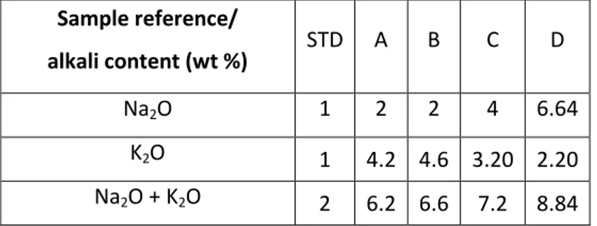
(11) Figure 3. SEM surface images of the enamels.. Figure 4. Enamelled ceramic substrate covered with molybdenum as back contact.. Molybdenum as back conductive contact was deposited on previously covered enamelled ceramic substrate using DC magnetron sputtering system (Alliance AC450). Figure 4 shown digital images of the different covered samples. These results are agreed with AFM and SEM images. Also, it can be observed visually the roughness increment with the alkali content. The different surface morphology of the ceramic substrates does.
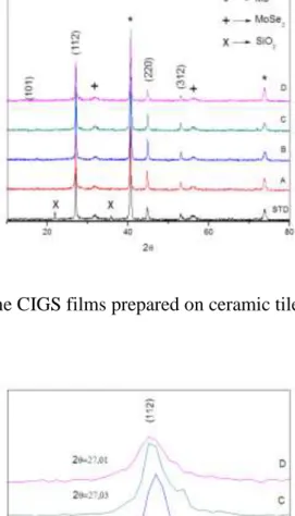
(12) not seem to harm the Mo back contact quality. The sheet conductivity was measured and exhibit Rsheet of 0.4 Ω/sq for all samples.. The XRD patterns shown in Figure 5 correspond to the synthesized absorber and confirms that the resulting layer contain the Cu(In0,7Ga0,3)Se2 compound (JCPDS 351102). The diffraction peaks labelled with hkl correspond to the CIGS phase, while Mo (JCPDS 42-1120) back contact reflections are indicated by stars. Extra peaks were also detected at 2θ: 31.82º and 53.07º that could be assigned to MoSe2 phase (JCPDS 200757). Reflections at 2θ = 21.8º, and 35.7º corresponds to SiO2 cristobalite (JCDPS 391425) coming from the enamel. Closer view of the CIGS main reflections (Fig.6), e.g. at ̴ 27º for hkl 112, show shifting towards higher 2θ degree with increasing of the alkali quantity in the composition (for samples B, C and D). These results is associated with contraction of the unit cell that could be due to the higher amount of Ga incorporation in the crystal lattice as rGa3+ (0.47Å) ˂ rIn3+ (0.62Å) tetrahedrally coordinated (Shannon et al., 1976) (Shannon 1976). So, it can be related that alkali doping favor the Ga insertion in the lattice. The sample A seems to be an exception from this declaration as the peaks shifts towards lower 2θ. We couldn´t explain this result. These outcomes, could be related with the alkali diffusion mechanism discussed in the literature as Na distribution along the grain boundaries (Salomé, et al. 2015). Recently, have been reported that K could also diffuses toward CIGS (Salomé, et al. 2015) and it is possible that other elements from the enamel might have the same behavior. It has been debated that K reduce the overall amount of Na and thus allowed a higher Cd diffusion into CdS without changing in microstructure of the CIGS layer and this increase the cell efficiency (Chirilă, et al. 2011). This statement settles the degree of.
(13) diffusion starting from the support, passing through the back contact and absorber coating and finally ending to the buffer layer (CdS).. Figure 5. XRD data of the CIGS films prepared on ceramic tile with applied enamels.. Figure 6. Zoomed section of XRD results..
(14) Figure 7. Cross section SEM images of CIGS device: STD, A, B, C and D. Figure 7 displays a cross section of the completed solar cells. The solar cells are composed by: enamel (bottom layer), followed by Mo coating (̴ 800nm), absorber CIGS layer (̴ 1,5µm), CdS buffer (̴ 20nm), zinc oxide (̴ 50 nm) and ITO window layer (̴ 400 nm). In all cases, dense and well attached homogeneous layers are observed. The lack of larger grains could be related with the use of amine compounds during the synthesis procedure and with the thermal treatment applied. It is demonstrated that the amine binders inhibit the crystal growth (Lee and Yong 2013), an undesirable effect for the solar cell morphology and thermal cycle with slopes and retention times is also advisable. Here, the amines are used to enhance the reduction process and further CIGS formation, an essential step in the proposed synthesis procedure. As a conclusion, it can be resumed that after thermal treatment do not appear any morphological differences as a function of the alkali content. In order to determine the dopant disuse mechanism, an EDX line profile was measured only for sample C (Fig. 8), selected as optimum. The results confirmed the presence of sodium and potassium in the enamel. The elemental detection corresponding of the rest of the layers was also correct. The diffusion of alkali elements from enamel towards the.
(15) CIGS absorber layer was not clear by the performed EDX analysis. This fact could be due to overlapping of the spectral lines of Na and Ga, and also K and In. So, the obtained result is ambiguous.. Figure 8. EDX line profile of the sample C.. The CIGS devices were optoelectronically characterized through current density-voltage (J-V) curves under AM1.5 global spectrum (Fig. 9). The photovoltaic behaviour is summarized in Table 2..
(16) Figure 9. Current density (mA/cm2) vs voltage (V).. Table 2. Summary of the optoelectronic parameters. Ceramic without enamel STD A B C D. Jsc (mA/cm2). Voc (mV). FF (%). Efficiency (%). 5.49. 89.5. 28.5. 0.1. 18.0 16.2 16.2 17.8 18.5. 319.3 320.8 332.1 344.3 323.9. 47.4 47.4 47.3 57.2 49.5. 2.7 2.5 2.6 3.5 3.0. The photovoltaic parameters for the investigated solar cells summarized in Table 2. In the Table a “ceramic tile without enamel” data is displays for comparative reason. It can be seen that 0.1 % conversion efficiency and inferior electrical parameters are obtained. It is evident that the enamel is compulsory cell component for the functionality of the photovoltaic tile. The best conversion efficiency is achieved for device C (Eff. = 3,5 %), which presents an improvement of 30 % in efficiency compared to STD sample. Also, the device performance parameters such as opencircuit voltage (Voc) and fill factor (FF) are improved, while the short-circuit current density (Jsc) is the same in both cases. Sample D present an improvement of 10 % in efficiency compared to STD sample and open circuit voltage and fill factor are slightly improved. The device B also showed a slight improvement in Eff, Voc and FF.
(17) parameters. Sample A shows very similar to the STD behavior. Only a slight improvement in the Voc is observed. As a conclusion, the combination of Na and K incorporation in the enamel has positive influence on optoelectronic properties of CIGS devices. Other groups also observed a significant increasing in Voc and FF when K was used (Jackson, et al. 2014; Adrian Chirilă 2013). Solar cell efficiencies and surface roughness were plotted vs % wt alkali concentration (Fig. 10). It can be observed the dependence of roughness with the alkali concentration. The trend is that efficiency increases with the concentration of alkaline until it reaches a maximum efficiency of 3.5% and a roughness of 18.9 nm. From this point, the efficiency begins to decrease.. Figure 10. Solar cell efficiencies vs enamel roughness and alkali content..
(18) 4. Conclusion The effect of alkali doping in the CIGS photovoltaic ceramic tile have been investigated. Several ceramic enamels with altered chemical composition in terms of amount of alkali metals have been tested and compared. It is demonstrated that enamel barrier layer is compulsory cell component for the functionality of the solar cell device. It was quantify the optimum amount of alkali (i.e 4% wt Na2O and 3.2 % wt. K2O) that provides the best conversion efficiency of 3.5 % for the CIGS solar cell. It was also observed that the alkali affect structurally by improving of Ga incorporation in the CIGS crystal lattice. The combination of both alkali (Na and K) increase an open-circuit voltage (Voc), fill factor (FF) and efficiency of the final device.. Acknowledgements The authors would like to acknowledge the financial support of the Spanish Ministry of Economy and Competitiveness under the program RETOS-COLABORACION (RTC2014-2294-3). We also appreciate the characterization assistance of Central Service of Scientific Instrumentation (SCIC) at the University Jaume I. We appreciate the Torrecid Group S.A. for the ceramic tiles supplying. The authors thank the group of A. Perez (Catalonia Institute for Energy Research-IREC) for the help in the solar cell assemble..
(19) References El Chaar, L., lamont, L.A., El Zein, N., 2011. Review of photovoltaic technologies. Renew. Sust. Energ. Rev. 15, 2165-2175. Park, S.-U., Sharma, R., Ashok, K., Kang, S., Sim, J.-K., Lee, C.-R., 2012. A study on composition, structure and optical properties of copper-poor CIGS thin film deposited by sequential sputtering of CuGa/In and In/(CuGa+In) precursors. J. Cryst. Growth 359, 1-10. Todorov, T.K., Cordoncillo, E., Sanchez-Royo, J.F., Carda, J., Escribano, P., 2006. CuInS2 Films for Photovoltaic Applications Deposited by a Low-Cost Method. Chem. Mater. 18, 31453150. Todorov, T.K., Gunawan, O., Gokmen, T., Mitzi, D.B., 2013. Solution-processed Cu(In,Ga)(S,Se)2absorber yielding a 15.2% efficient solar cell. Prog. Photovoltaics 21, 8287. Jung, S., Ahn, S., Yun, J.H., Gwak, J., Kim, D., Yoon, K., 2010. Effects of Ga contents on properties of CIGS thin films and solar cells fabricated by co-evaporation technique. Curr. Appl. Phys. 10, 990-996. Contreras, M.A., Romero, M.J., Noufi, R., 2006. Characterization of Cu(In,Ga)Se2 materials used in record performance solar cells. Thin Solid Films 511-512, 51-54. Reinhard, P., Buecheler, S., Tiwari, A.N., 2013. Technological status of Cu(In,Ga)(Se,S)2-based photovoltaics. Sol. Energ. Mat. Sol. C. 119, 287-290. Zhang, K., Yang, C.-l., Yin, L., Liu, Z., Song, Q.-m., Luo, H.-l., Xiong, Z.-y., Xu, M.-m., Xiao, X.-d., 2014. Fabricating highly efficient Cu(In,Ga)Se2 solar cells at low glass-substrate temperature by active gallium grading control. Sol. Energ. Mat. Sol. C. 120, 253-258. Furue, S., Ishizuka, S., Yamada, A., Iioka, M., Higuchi, H., Shibata, H., Niki, S., 2013. Cu(In,Ga)Se2 solar cells and mini-modules fabricated on thin soda-lime glass substrates. Sol. Energ. Mat. Sol. C. 119, 163-168. Park, S.J., Lee, E., Jeon, H.S., Ahn, S.J., Oh, M.-K., Min, B.K., 2011. A comparative study of solution based CIGS thin film growth on different glass substrates. Appl. Surf. Sci. 258, 120-125. Reinhard, P., Pianezzi, F., Kranz, L., Nishiwaki, S., Chirilă, A., Buecheler, S., Tiwari, A.N., 2015. Flexible Cu(In,Ga)Se2solar cells with reduced absorber thickness. Prog. Photovoltaics 23, 281-289. Chirilă, A., Buecheler, S., Pianezzi, F., Bloesch, P., Gretener, C., Uhl, A.R., Fella, C., Kranz, L., Perrenoud, J., Seyrling, S., Verma, R., Nishiwaki, S., Romanyuk, Y.E., Bilger, G., Tiwari, A.N., 2011. Highly efficient Cu(In,Ga)Se2 solar cells grown on flexible polymer films. Nat. Mater. 10, 857-861. Caballero, R., Kaufmann, C.A., Eisenbarth, T., Unold, T., Klenk, R., Schock, H.-W., 2011. High efficiency low temperature grown Cu(In,Ga)Se2 thin film solar cells on flexible substrates using NaF precursor layers. Prog. Photovoltaics 19, 547-551. Pianezzi, F., Chirilă, A., Blösch, P., Seyrling, S., Buecheler, S., Kranz, L., Fella, C., Tiwari, A.N., 2012. Electronic properties of Cu(In,Ga)Se2solar cells on stainless steel foils without diffusion barrier. Prog. Photovoltaics 20, 253-259. Liang, X., Zhu, H., Chen, J., Zhou, D., Zhang, C., Guo, Y., Niu, X., Li, Z., Mai, Y., 2016. Substrate temperature optimization for Cu(In, Ga)Se2 solar cells on flexible stainless steels. Appl. Surf. Sci. 368, 464-469. Wuerz, R., Eicke, A., Kessler, F., Paetel, S., Efimenko, S., Schlegel, C., 2012. CIGS thin-film solar cells and modules on enamelled steel substrates. Sol. Energ. Mat. Sol. C. 100, 132-137. Fraga, D., Stoyanova Lyubenova, T., Martí, R., Calvet, I., Barrachina, E., Carda, J.B., 2016. Ecologic ceramic substrates for CIGS solar cells. Ceram. Int. 42, 7148-7154. Calvet, I., Barrachina, E., Martí, R., Fraga, D., Stoyanova Lyubenova, T., Carda, J.B., 2015. Development of photovoltaic ceramic tile based on CZTSSe absorber. Mater. Lett. 161, 636-639..
(20) Fraga, D., Lyubenova, T.S., Rey, A., Calvet, I., Martí, R., Carda, J.B., 2015. Ceramic Enamels as New Back Contacts for Cu (In, Ga) Se2-Based Photovoltaic Tile. Int. J. Appl. Ceram. Tec. 12, 728-737. Calvet, I., Barrachina, E., Martí, R., Fraga, D., Lyubenova, T.S., Carda, J.B., 2015. Synthesis, deposition and crystal growth of CZTS nanoparticles onto ceramic tiles. Bol. Soc. Esp. Ceram. V. 54, 175-180. Salomé, P.M.P., Rodriguez-Alvarez, H., Sadewasser, S., 2015. Incorporation of alkali metals in chalcogenide solar cells. Sol. Energ. Mat. Sol. C. 143, 9-20. Theelen, M., Daume, F., 2016. Stability of Cu(In,Ga)Se2 solar cells: A literature review. Sol. Energy 133, 586-627. Rudmann, D., Brémaud, D., da Cunha, A.F., Bilger, G., Strohm, A., Kaelin, M., Zogg, H., Tiwari, A.N., 2005. Sodium incorporation strategies for CIGS growth at different temperatures. Thin Solid Films 480-481, 55-60. Eid, J., Usman, A., Gereige, I., Duren, J.V., Lyssenko, V., Leo, K., Mohammed, O.F., 2015. Ultrafast pump-probe reflectance spectroscopy: Why sodium makes Cu(In,Ga)Se2 solar cells better. Sol. Energ. Mat. Sol. C. 140, 33-37. He, X., Liu, J., Ye, Q., Luo, K., Jiang, Y., Liao, C., Ouyang, L., Zhuang, D., Mei, J., Lau, W., 2016. The role of Na incorporation in the low-temperature processed CIGS thin film solar cells using post deposition treatment. J. Alloy. Compd. 658, 12-18. Hsu, C.-H., Su, Y.-S., Wei, S.-Y., Chen, C.-H., Ho, W.-H., Chang, C., Wu, Y.-H., Lin, C.-J., Lai, C.-H., 2015. Na-induced efficiency boost for Se-deficient Cu(In,Ga)Se2solar cells. Prog. Photovoltaics 23, 1621-1629. Moriwaki, K., Nomoto, M., Ishizuka, S., Mukai, A., Sato, K., Kobayashi, H., Niki, S., 2015. Effects of alkali-metal block layer to enhance Na diffusion into Cu(in,Ga)Se2 absorber on flexible solar cells. Sol. Energ. Mat. Sol. C. 133, 21-25. Wuerz, R., Eicke, A., Kessler, F., Rogin, P., Yazdani-Assl, O., 2011. Alternative sodium sources for Cu(In,Ga)Se2 thin-film solar cells on flexible substrates. Thin Solid Films 519, 72687271. Reinhard, P., Bissig, B., Pianezzi, F., Avancini, E., Hagendorfer, H., Keller, D., Fuchs, P., Döbeli, M., Vigo, C., Crivelli, P., Nishiwaki, S., Buecheler, S., Tiwari, A.N., 2015. Features of KF and NaF Postdeposition Treatments of Cu(In,Ga)Se2 Absorbers for High Efficiency Thin Film Solar Cells. Chem. Mater. 27, 5755-5764. Laemmle, A., Wuerz, R., Powalla, M., 2015. Investigation of the effect of potassium on Cu(In,Ga)Se2 layers and solar cells. Thin Solid Films 582, 27-30. Lee, M., Lee, S.M., Jung, S., Ahn, S., Cho, J.-S., Park, J., Eh, Y., Gwak, J., Shin, K., Yoon, K., Cho, Y.S., Yun, J.H., 2015. Highly efficient flexible CuIn0.7Ga0.3Se2 solar cells with a thick Na/Mo layer deposited directly on stainless steel. Appl. Surf. Sci. 346, 562-566. Becerril-Romero, I., Giraldo, S., López-Marino, S., Placidi, M., Sánchez, Y., Sylla, D., PérezRodríguez, A., Saucedo, E., Pistor, P., 2016. Vitreous enamel as sodium source for efficient kesterite solar cells on commercial ceramic tiles. Sol. Energ. Mat. Sol. C. 154, 11-17. Casasola, R., Rincón, J.M., Romero, M., 2011. Glass–ceramic glazes for ceramic tiles: a review. J. Mater. Sci. 47, 553-582. Nandi, V.S., Raupp-Pereira, F., Montedo, O.R.K., Oliveira, A.P.N., 2015. The use of ceramic sludge and recycled glass to obtain engobes for manufacturing ceramic tiles. J. Clean. Prod. 86, 461-470. Siligardi, C., Lusvarghi, L., Giolli, C., Scrivani, A., Venturelli, D., 2014. Recycling in ceramic glazes of zirconia overspray from thermal barrier coatings manufacturing. J. Eur. Ceram. Soc. 34, 147-154. Martí, R., Oliveira, L., Lyubenova, T.S., Todorov, T., Chassaing, E., Lincot, D., Carda, J.B., 2015. Preparation of Cu(In,Ga)Se2 photovoltaic absorbers by an aqueous metal selenite coprecipitation route. J. Alloy. Compd. 650, 907-911..
(21) Shannon, R.D., 1976. Revised Effective Ionic Radii and Systematic Studies of Interatomic Distances in Halides and Chalcogenides. Acta Crystallogr. A32, 751-767. Lee, D., Yong, K., 2013. Non-vacuum deposition of CIGS absorber films for low-cost thin film solar cells. Korean J. Chem. Eng. 30, 1347-1358. Jackson, P., Hariskos, D., Wuerz, R., Wischmann, W., Powalla, M., 2014. Compositional investigation of potassium doped Cu(In,Ga)Se2solar cells with efficiencies up to 20.8%. Phys. Status Solidi (RRL) 8, 219-222. Adrian Chirilă, P.R., Fabian Pianezzi, Patrick Bloesch, Alexander R. Uhl, Carolin Fella, Lukas Kranz, Debora Keller, Christina Gretener, Harald Hagendorfer, Dominik Jaeger, Rolf Erni, Shiro Nishiwaki, Stephan Buecheler and Ayodhya N. Tiwari, 2013. Potassiuminduced surface modification of Cu(In,Ga)Se2 thin films for high-efficiency solar cells. Nat. Mater. 12, 1107–1111..
(22)
Figure


+6


Documento similar
In this respect, a comparison with The Shadow of the Glen is very useful, since the text finished by Synge in 1904 can be considered a complex development of the opposition
In the previous sections we have shown how astronomical alignments and solar hierophanies – with a common interest in the solstices − were substantiated in the
While Russian nostalgia for the late-socialism of the Brezhnev era began only after the clear-cut rupture of 1991, nostalgia for the 1970s seems to have emerged in Algeria
The concept of breakdown probability profile is useful to describe the break- down properties of any estimate obtained through resampling, not just the bagged median or the
1. S., III, 52, 1-3: Examinadas estas cosas por nosotros, sería apropiado a los lugares antes citados tratar lo contado en la historia sobre las Amazonas que había antiguamente
Abstract: Transepidermal water-loss (TEWL), stratum-corneum hydration (SCH), erythema, elas- ticity, pH and melanin, are parameters of the epidermal barrier function and
MD simulations in this and previous work has allowed us to propose a relation between the nature of the interactions at the interface and the observed properties of nanofluids:
Government policy varies between nations and this guidance sets out the need for balanced decision-making about ways of working, and the ongoing safety considerations
