Abstract—Hysteresis in power amplifiers is investigated in detail with the aid of an efficient analysis method, compatible with commercial harmonic balance. Suppressing the input source and using, instead, an outer-tier auxiliary generator, together with the Norton equivalent of the input network, analysis difficulties associated with turning points are avoided. The turning point locus in the plane defined by any two relevant analysis parameters is obtained in a straightforward manner, using a geometrical condition. The hysteresis phenomenon is demonstrated to be due to a nonlinear resonance of the device input capacitance under near optimum matching conditions. When increasing the drain bias voltage, some points of the locus degenerate into a large-signal oscillation that cannot be detected with a stability analysis of the dc solution. In driven conditions, the oscillation will be extinguished either through synchronization or inverse Hopf bifurcations in the upper section of the multivalued curves. For an efficient stability analysis, the outer-tier method will be applied in combination with pole-zero identification and Hopf bifurcation detection. Departing from the detected oscillation, a slight variation of the input network will be carried out so as to obtain a high efficiency oscillator able to start-up from the noise level. All the tests have been carried out in a Class-E GaN PA with measured 86.8% PAE and 12.4 W output power at 0.9 GHz.
Index Terms— Bifurcation, class-E, harmonic balance (HB), GaN, hysteresis, power amplifier, stability, UHF.
I. INTRODUCTION
LASS-E power amplifiers (PAs) have been receiving increased attention, due to their potential for simultaneously providing linear and efficient amplification when employed in bias- or load-modulation architectures [1]. However, it is not uncommon to observe instability phenomena in these amplifiers, some of which have been reported in [2-3]. Indeed, hysteresis can be found under near optimum input matching conditions, which gives rise to sudden transitions or jumps [2, 4-5] between different sections of the power-transfer curve when either increasing or
This paper is an expanded version from the IEEE MTT-S International Microwave Symposium, Phoenix, AZ, USA, 17-22 May 2015. Manuscript received July 01, 2015.
The authors are with the Communications Engineering Department, University of Cantabria, Escuela Técnica Superior de Ingenieros Industriales y de Telecomunicación (ETSIIT), 39005 Santander, Spain (e-mail: [email protected]; [email protected]; [email protected]).
decreasing the input power. From a geometrical viewpoint, the hysteresis is due to the presence of turning points or infinite-slope points [5-6] in the solution curve, which, in designs based on commercial harmonic balance (HB), have been detected [2,4,7] with the aid of an auxiliary generator (AG). However, there is little insight into the mechanism for the appearance of these turning points, often observed when approaching the intended operation conditions [2-3].
In the GaN HEMT-based Class-E power amplifier (PA) studied here, the nonlinear input capacitance resonates with the inductive input matching network, as will be demonstrated analytically. For an accurate prediction/suppression of the phenomenon, the outer-tier method presented in [8] will be adapted to the case of the PA with hysteresis, which will allow tracing the multivalued solution curves in an efficient manner, with no need for parameter switching [7,9-11]. This method will also enable a direct calculation of the turning point locus in terms of any practical analysis parameter, such as the gate bias voltage, the input matching capacitor or the input power, by simply imposing a geometrical condition [8].
The observation of the hysteresis phenomenon studied in detail in [3] is often empirically associated with the onset of oscillations under a relatively small variation of the circuit parameters or element values. This paper expands [3] by studying the relationship between these two phenomena, apparently quite different, which will be done through a detailed analysis of the impact of the drain bias voltage (VDS)
on the turning point locus. As will be shown, the turning point locus, which at zero drain bias voltage is solely due to the input nonlinear capacitance, spreads over lower input power values. From certain VDS, some discrete points of the locus
reach zero input power and degenerate into free-running oscillations that coexist with a stable dc solution. As will be demonstrated in this work, under most input matching conditions, this oscillation cannot be detected with any standard stability analysis, as it coexist with a stable dc regime even for gate bias voltages above conduction threshold. When injecting the input power, it will give rise to a stable self-oscillating mixer regime, coexisting with the stable periodic solution at the frequency of the input source. The oscillation will be extinguished either through synchronization [5,12], for input frequencies near the free-running oscillation frequency, or through inverse Hopf-type bifurcations [5-6,12].
This paper expands [3] with a detailed analysis of the oscillatory solution and the mechanisms for the oscillation extinction. Synchronization of an oscillation with an injection
Hysteresis and Oscillation in High Efficiency
Power Amplifiers
Jesús de Cos, Student Member, IEEE, Almudena Suárez, Fellow, IEEE, and José A. García, Member,
IEEE
source occurs at particular types of turning points, at which a local-global bifurcation takes place [5,12-13], also known as a limit cycle on saddle-node in the Poincaré map. Therefore, these bifurcations will belong to the turning point locus that is efficiently detected with the outer-tier method. Another contribution with respect to [3] is the derivation of a methodology for the Hopf bifurcations, which will be carried out combining this outer-tier method with a zero-amplitude oscillation condition, imposed with the aid of a small-signal AG [2,5,11]. Because the Hopf bifurcations may take place in any section of the multivalued curves, the combination of this limit-oscillation condition with the outer-tier method is very advantageous, since it avoids the need for a large-signal non-perturbing AG to sustain solutions in sections of the multivalued curve to which commercial HB does not converge by default. Another extension with respect to [3] will be the combination of the outer-tier methodology with pole-zero identification to obtain the whole evolution of the stability properties of the multivalued solution curve in a single sweep, with no need to perform any parameter switching.
The ease of application of the bifurcation detection methodologies will allow an in-depth investigation of the impact of the most relevant parameters, such as the gate bias voltage, the input matching capacitor and the input power, on the global stability of the PA. This will provide insight into the various instability mechanisms observed in the PA and the relationships between them. Another expansion of this work with respect to [3] is the derivation of an oscillator design methodology based on a controlled selection of the element values that should turn the Class-E PA into a highly efficient oscillator [14], able to start-up from the noise level. RF power oscillators may be of interest for the implementation of high power density and fast response resonant dc/dc converters [15], wireless power transmission links [16], etc.
The paper is organized as follows. Section II presents the study of the hysteresis using a high efficiency Class-E PA demonstrator. The stability of the resulting multivalued curves is analyzed in Section III, with the aid of the outer-tier method. In Section IV, the detected free-running oscillation is related to the hysteresis phenomenon. Finally, a high efficient RF power oscillator is presented.
II. STUDY OF HYSTERESIS A. Class-E power amplifier demonstrator
A power amplifier (PA) at 900 MHz was designed in [3] with the aim of obtaining a very high value of power-added efficiency (PAE). Among many choices, the high efficiency of Class-E operation was exploited, minimizing the switching loss associated with the transistor output capacitance. A CGH35030F GaN on SiC HEMT from Cree Inc. was selected as the switching element, due to the very low value of its on resistance times output capacitance product (Ron⋅Cout) and high
breakdown voltage (over 120 V).
Initially, the transistor was experimentally characterized in Arlon 25N substrate (εr = 3.38, h = 30 mil, t = 70 μm) for a
typical drain bias voltage VDS = 28 V, after verifying the peak
value of the voltage waveform, 3.562⋅VDS [17], would stay
below the process breakdown figure. The gate bias voltage was set slightly below pinch-off: VGS = −3.3 V, while the
output capacitance (Cout) and off-state resistance (Roff) were
estimated from the measured S22 parameter [3]. The measured values of on-state resistance, output capacitance and off-state resistance at 900 MHz are 0.6 Ω, 3.5 pF and 5.1 kΩ, respectively. An ideal dc voltage source, a capacitor and a resistance were added to the already accurate and reliable Cree's proprietary large-signal transistor model to finely adjust, respectively, the values of the gate threshold voltage, output capacitance and off-state resistance in simulations to the measured device parameters.
As a first approximation, the output network was designed based on the optimum or nominal conditions for a 50% switching duty cycle and maximum output power found by Raab [17]: 0.1836 0.2116 opt out opt out R C X C ω ω = = . (1)
Unfortunately, the required inductance value in the classic Class-E output network may be too large to be obtained with commercially available coils, as their self-resonant frequency could be below the most significant higher order harmonics to be properly terminated [18]. One not uncommon solution for lumped-element Class-E implementations at UHF band [19] is to take advantage of a high-Q coil with a self-resonant frequency in between the second and third order harmonics [20], so that a high enough impedance (either inductive or capacitive) is presented. Here, a slightly different strategy was adopted. A smaller inductor, Lout in the schematic of Fig. 1(a),
was selected, with an associated smaller equivalent series resistance at dc, trying to minimize its contribution to the circuit conduction loss [21]. In addition, advantage was taken from its higher self-resonant frequency at about the fifth order harmonic for properly terminating most of them. The optimum reactance value in (1) was adjusted with a section of microstrip transmission line, while the capacitor Cout to ground allowed
synthesizing the desired Ropt. The reflection coefficient of the
resulting output network, Γout, is represented in the Smith chart
in Fig. 1(b), together with the simulated load-pull contours for drain efficiency (solid line) and output power (dashed line). The contours were obtained at the fundamental frequency with ideal terminations (open circuit) to other harmonics.
a) Is Zo Zo Cin Lin Lout Cout Cbk Lck Rg VGS VDS Lck Cs s Γout 8.1º 22.6º b) fund 2nd 3rd 4th 5th 6th 7th 8th Γout 80% 85% 40 dBm 42 dBm L.E. Value Cin 13 pF Lin 1.65 nH Lout 5 nH Cout 2.4 pF || 2 pF Cs 100 pF Lck 150 nH c)
Fig. 1. (a) Schematic of the Class-E power amplifier demonstrator [3]. Values in the table are for Colcraft Air Core inductors and ATC 100B capacitors. (b) Simulated reflection coefficient of the output network and load-pull contours. (c) Photograph of the measurement setup.
A typical single low-pass section was used to match the input of the PA to increase the gain and thus the PAE. The experimental value of the input matching capacitor Cin was
10 pF, a bit lower than the one used in simulations. A resistance was introduced in the gate biasing path to improve stability at lower frequencies. Although not included in the schematic for simplicity, a bank of high-valued capacitors (1 nF, 10 nF, 100 nF, 1 μF and 10 μF) were added in the gate and drain dc lines. The employed measurement setup is shown in Fig. 1(c). As can be seen, two low-pass filters with cutoff frequency at 1 GHz are included just before the power sensor to exclude any possible contribution of harmonics different than the fundamental to the output power. Table I includes the measurement results and a comparison with other RF Class-E power amplifiers in the literature.
TABLEI
RFCLASS-E POWER AMPLIFIERS IN THE LITERATURE
Freq
(GHz) PAE (%) Pout (dBm) Gain (dB) Transistor type Reference
0.37 84 46.5 14 HEMT GaN [22]
0.434 78.6 36.9 >15 LDMOS [23]
0.8 80.6 46.9 16.3 HEMT GaN [24]
0.9 86.8 40.9 19.5 HEMT GaN This work
1 73 29.7 - MESFET GaAs [25]
1.99 82.1 22.8 >10 HEMT GaAs [26]
2 74 40.5 12.6 HEMT GaN [27]
2.14 74 40.8 14 HEMT GaN [28]
In Fig. 2, the power-added efficiency of the amplifier is represented versus the input power (Pin). When increasing Pin a
jump is observed for 10 dBm. When decreasing the input power there is no longer a jump at 10 dBm but at a lower value of about 7 dBm. This behavior is evidence of hysteresis. Looking at the simulated curve, two turning points or infinite slope points are found, responsible for the undesired
phenomenon. The multivalued curve has been traced with the method described in Subsection II-C. Note that default harmonic balance is unable to pass through the infinite slope points. 5 10 15 20 25 0 20 40 60 80 100 Input power (dBm) Power -added efficiency (%) S1 S2 S3
Fig. 2. Power-added efficiency of the Class-E PA versus input power. Solid lines are the results of a default simulation in commercial HB. The curve is completed (dashed line) with the method described in Subsection II-C. Symbols are measurements.
B. Study of the parametric hysteresis
The hysteresis phenomenon observed in the solution curve of Fig. 2 is caused by a nonlinear resonance of the device input capacitance (due to the gate-to-source and the input-reflected gate-to-drain Miller capacitances [29]) with the inductive impedance of the input network. An analytical study will be carried out short-circuiting the transistor drain and source terminals, and modeling the transistor input with only its nonlinear gate-to-channel capacitance, as depicted in Fig. 3(a). The input matching network considered is the one in the original design in Fig. 1(a), but neglecting the impact of the parasitics in the lumped elements, the transmission line and the RF choke. Is Zo Cin Lin Vs V Q(V) a) 0 5 10 15 0.5 1 1.5 2 2.5 3 3.5 4 Input power (dBm)
Gate voltage amplitude
(V ) T T T T Analytical Simulation b)
Fig. 3. (a) Circuit used to study the input network of the PA. (b) Comparison between the analytical result and HB simulation. The turning points have been marked.
A describing function of the corresponding nonlinear charge
q(t) will be used, assuming a sinusoidal input waveform
( ) cos( )
s s in
i t =I ω t+φ . This allows formulating the circuit at the fundamental frequency:
[
2 2 ( ) ( ) ( ) 0. j o s in in in o in in in in H V Z I e L Q V j Z C V L C Q V Q V φ ω ω ω ≡ − − + − + = (2)where a complex function H ≡0 has been defined. Calculating the derivatives of the real and imaginary part of (2) with respect to V and φ, the Jacobian matrix is
2 2 2 2 1 ' ( ' ') ( in in ) in o in in in in H in o in in in in in in L Q Z C L C Q Q J Z C V L C Q Q L Q V ω ω ω ω ω ω − − + = − + − (3) where Q dQ dV'= / . The singularity condition is
(
)(
)
2 2 2 2 2 det( ) ( ' 1)( ) ( ) ' ' 0. H in in in in in o in in in in in in in in J L Q L Q V Z C L C Q Q C V L C Q Q ω ω ω ω ω = − − − − − + − + = (4)The expression of the input power (in dBm) is obtained squaring and adding the real and imaginary parts of (2):
2 2 2 2 10 2 10 10log ( ) ( ) ( ) 30 10log (8 ). in in in in o in in in in o P V L Q Z C V L C Q Q Z ω ω ω = − + − + + − (5)
Results obtained with the analytical formulation (5) and with harmonic balance are compared in Fig. 3(b). As shown in the figure, the simplified analytical study of the input network is able to predict the existence of two turning points. Each of these two turning points fulfills the condition (4). Discrepancies come from contributions of the extrinsic parameters inside the transistor model, not considered when calculating the nonlinear charge in the frequency domain.
C. Analysis method
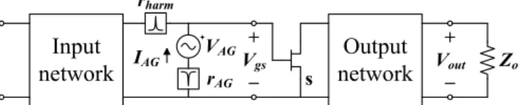
The multivalued solution curves will be obtained by adapting the outer-tier method, developed in [8] for injection-locked oscillators, to the case of PAs. The input generator is suppressed using, instead, an auxiliary generator (AG) [5,11] at the gate terminal, which operates at the input frequency (Fig. 4). This enables the calculation of the outer-tier admittance function Ygs =IAG,1/VAG, where IAG,1 is the current
through the AG at the fundamental frequency and VAG is the
AG amplitude. The admittance function Y will be combined gs with the Norton equivalent of the input network at the gate terminal, which can be calculated from its scattering matrix. The combination of both functions provides an outer-tier equation, which relates the gate voltage amplitude at the
fundamental frequency V (agreeing with VAGgs ) and the input generator current Is: s eq gs I = Y V , (6) where
[
11 22]
0[
11 22]
21 1 ( ) 1 ( ) 2 gs eq S S Y S S Y Y S − + ∆ − + − − ∆ − = .To obtain a power-transfer curve, VAG is swept, calculating
the function Ygs =IAG,1/VAG at each sweep step. The input generator current Is enabling each voltage VAG is determined
with (6). Note that the outer-tier equation (6) is combined with the full HB system, acting as an inner tier, so all the circuit variables are available at each sweep step. Therefore, relevant magnitudes such as the output power or efficiency can be calculated in a straightforward manner. The outer-tier method provides the multivalued solution curves with no need of parameter switching unlike previous works [5,30].
Input
network
network
Output
rharm rAG VAGV gs IAG s Vout Zo
Fig. 4. Circuit used for obtaining the outer-tier admittance function Ygs. The method has been applied to complete the solution curve in Fig. 2 and to trace the whole one in Fig. 3 in simulation. It has also been used to analyze the impact of the gate bias voltage (VGS) on the PAE curves (Fig. 5). It must be
emphasized that here a complete description of the input network is considered, including full models of passive components, the transmission line and the RF choke.
-100 -5 0 5 10 15 20 25 30 20 40 60 80 100 Input power (dBm) Power -added efficiency (%) -2.8 V -3 V -3.3 V -3.5 V -3.7 V -4 V Turning point locus VGS = -2.8 V -3 V -3.3 V -3.5 V -3.7 V -4 V
Fig. 5. Power-added efficiency of the Class-E PA versus input power for some values of the gate bias voltage. Solid lines are simulation results obtained with the outer-tier method. The dashed line superimposed is the turning point locus. Symbols are measurements.
The evolution of the hysteresis region versus a relevant parameter μ, affecting the nonlinear resonance, can be efficiently investigated by tracing the turning point locus in the plane defined by the particular parameter μ and the input power, following the method in [8]. One of these analysis
parameters (μ) is VGS, already considered in the analysis of Fig.
5, and the other is the input matching capacitance Cin. To
obtain the turning point locus one should consider the surface ( , )µVgs Y Veq gs
∑ = described by (6) on the plane defined by μ and V . The turning point locus is the set of points of Σ gs satisfying zero partial derivative with respect to V , that is, gs the zero-level contour:
{
( , ) 2: ( , ) / 0}
gs gs gs
T = µV ∈ ∂ ∑ µV ∂V = . (7)
The locus resulting from (7) when using VGS as parameter
has been superimposed on the solution curves of Fig. 5 in dashed line. As can be seen, the locus passes through all the turning points of the solution curves. Fig. 6 shows the same turning point locus represented in the plane defined by VGS and Pin. The hysteresis region decreases with VGS and vanishes to
zero near the pinch-off voltage Vp. Measurement points are
superimposed.
To get some insight into the reasons for the observation of the phenomena in the lower VGS range, one must take into
account that in these subthreshold conditions the transistor gain increases with the excitation amplitude. As a result, the conductance function, when looking into the circuit nonlinear section from the AG terminals (Fig. 4), initially increases with the excitation amplitude and then decreases as expected in any physical device. Because the frequency of each coexisting solution agrees with the frequency of the input source, the phase shift between the driving source and the AG excitation voltage is a relevant variable. Fig. 7 shows the contour plots of total conductance and total susceptance equal to zero in the plane defined by the AG phase and amplitude, when the input power is set to 8 dBm. The total conductance/susceptance functions include contributions from both the linear and nonlinear sections of the PA at the observation node. There is a steady-state solution for each intersection of the two contour plots, so three steady-state solutions S1, S2, S3 coexist for this Pin value, in agreement with the results of Fig. 2. The high dependence of the total admittance function on the excitation amplitude gives rise to two zero susceptance contours and a bending of the zero conductance contour. This favors the occurrence of three intersections, corresponding to the three solutions that coexist for the particular Pin value.
-7 -6 -5 -4 -3 -2 -10 -5 0 5 10 15 20 25 30
Gate bias voltage (V)
Input power
(dBm
)
Vp
Fig. 6. Turning point locus in the plane defined by the gate bias voltage and the input power. Square symbols are measurements (for the particular value VGS = −3.3 V, it was also measured when decreasing Pin).
Next, the impact of the matching capacitance Cin will be
analyzed. In [3], the turning point locus was represented in the plane defined by VGS and V for different values of Cings . This allowed to suppress the undesired phenomenon. The final measurements results for an experimental capacitor value of 8.2 pF are 85.4% of PAE, 16.1 dB of power gain and 12.3 W of output power. Here, the turning point locus is represented in the plane defined by Cin and Pin, for different values of the
drain bias voltage (VDS). For VDS = 0 V, one obtains the
small-size locus in Fig. 8, existing for capacitor values between 31.3 pF and 52.3 pF. This locus characterizes the hysteresis phenomenon that is solely due to the nonlinear input capacitance, as studied in Subsection II-B. For each constant
Cin value, the locus provides the input power values at which the hysteresis jumps are produced. When increasing VDS, there
is also an influence of the nonlinear transfer characteristic
IDS(VGS) [29], and the locus expands over larger intervals of Cin
and Pin. From a certain VDS value, the locus decays to zero
value and this will give rise to an oscillation phenomenon. For a detailed analysis, the typical drain bias voltage VDS = 28 V
will be considered, as this is the one selected for the high efficiency design. -2000 -180 -160 -140 -120 -100 -80 -60 -40 0.5 1 1.5 2 2.5 3 AG phase (deg) AG amplitude (V ) {GT = 0} {BT = 0} S1 S2 S3
Fig. 7. Zero-level contours of the total conductance (GT) and susceptance (BT) obtained when introducing an AG at the gate terminal for VGS = −3.3 V
corresponding solution curve of Fig. 2. Note the multivalued nature of the contours. 101 102 0 2 4 6 8 10 12 14
Input matching capacitor (pF)
Input power (mW ) 0 V 4 V 12 V 28 V 2·102 38.3 41.4 10.9 22 30.1
Quality factor of the input network
3·101 5·101
Fig. 8. Evolution of the turning point locus versus the drain bias voltage, represented in the plane defined by Cin and Pin. This diagram illustrates the
connection between the hysteresis and a free-running oscillation. The values in the upper axis correspond to the quality factor of the input network for each Cin value in the label.
Fig. 9(a) presents the turning point locus for VDS = 28 V. In
the results presented so far and in [3], a model of the input matching capacitor, including the parasitics, is used. For those analysis using Cin as parameter, a lower value is selected, for
which no hysteresis is found, and then an ideal capacitor ∆Cin
is connected in parallel. In this way, the value of the capacitance can be varied continuously. As can be seen in Fig. 9(a), there are two capacitor values for which the turning point locus reaches the axis (zero input power value). At these two particular points, Os and Ou, the locus should degenerate into
two free-running oscillations. An interesting fact is that the dc solution of the power amplifier is stable for all the capacitor values considered in Fig. 9(a), as the device is biased below pinch-off. In measurements, the dc solution was found stable for all the capacitor values tested, even when biasing the transistor above pinch-off. In simulations, the dc solution only becomes unstable in a very reduced region when biasing the transistor above pinch-off for large capacitor values. Therefore, the oscillations in Fig. 9(a) cannot be detected with a small-signal stability analysis of the PA. The relationship between the hysteresis and the oscillations obtained in Fig. 9(a) will be investigated with a stability analysis methodology adapted to the case of multivalued solutions.
101 102 0.7 0.75 0.8 0.85 0.9 0.95 1 Autonomous frequency (GHz ) 2·102 Os Ou Cin0 101 102 5 10 15 20 25 30 35 40 45
Input matching capacitor (pF)
Output power (dBm ) 2·102 Os Ou Cin0
Input matching capacitor (pF)
a) b) c) 101 102 0 2 4 6 8 10 12 14
Input matching capacitor (pF)
Input power (mW ) 2·102 Section 2 Section 3 Section 1 Os Ou CT CT CT CT
Fig. 9. Synchronization with free-running oscillations. (a) Turning point (solid line) and Hopf bifurcation (dashdotted line) loci: input power versus the input matching capacitor value. (b) Output power versus Cin in
free-running operation (Pin = 0 W). (c) Autonomous frequency versus Cin in
free-running operation. Note that the Cin values for which the autonomous
frequency is 0.9 GHz agree with the degenerate points of the turning point locus (Pin = 0 W). Stable (unstable) sections in solid (dashed) line. Square
symbols are measurements (attention was only paid to values close to Cin0).
III. STABILITY ANALYSIS THROUGH THE MULTIVALUED SOLUTIONS
The application of a complementary stability analysis through multivalued solution curves is demanding since HB will converge to the default solution, usually corresponding to
the one with the smallest output power, or will not converge at all. To cope with this problem, the outer-tier method will be combined with pole-zero identification [31-32] and bifurcation detection [2,5,11,30,33], as explained in the following.
A. Stability analysis
In the analysis of Fig. 4, the whole solution curve is traced suppressing the input source and using an AG to calculate the outer-tier admittance function considered in (6). Then, the curve is obtained by sweeping the AG amplitude VAG in HB.
The input power is calculated from VAG using the Norton
equivalent. Thus, turning points only result from the composition of any of the circuit state variables with the input power. In this way, the equivalent system (6) provides the same solutions that would be obtained with a suitably initialized HB system. Therefore, the stability can be analyzed with the AG connected to the circuit, instead of the driving source (Fig. 4). Note that unlike other previous methods the AG does not fulfil a non-perturbation condition. In the presence of this AG, a small-signal current source at the incommensurate frequency Ω is introduced at a sensitive circuit node (the gate terminal). This source is used to linearize the circuit about the large-signal periodic regime at each HB sweep step with the conversion-matrix approach [34-35]. The following calculation is performed:
( ) ( ) ( , ) ( , ) ( , ) s AG eq AG gs n AG o AG n AG I V Y V V V V H V I V = Ω Ω = Ω , (8)
where Vn is the gate node voltage and In is the current of the small-signal source. The stability analysis is performed applying pole-zero identification [31-32] to the function (8) obtained for each VAG value. For the stability analysis to work
properly, a difference with respect to [3] and [8] must be remarked: the filter r_harm should only stop the frequency of the input generator (0.9 GHz), allowing for a proper impedance termination at other harmonic mixing terms.
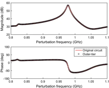
For validation, the stability analysis has been applied to the solution point S1 in Figs. 2 and 7. Note that it is a point to which the HB method converges by default, as gathered from the solid line simulation in Fig. 2. The transfer functions obtained with the original circuit and performing the topology change (suppression of the input source plus introduction of the outer-tier AG) are compared in Fig. 10. The results in the two different analysis conditions are overlapped.
0.8 0.85 0.9 0.95 1 1.05 1.1 20 30 40 50 60 Perturbation frequency (GHz) Magnitude (dB ) 0.8 0.85 0.9 0.95 1 1.05 1.1 -180 -90 0 90 180 Perturbation frequency (GHz) Phase (deg
) Original circuitOuter-tier
Fig. 10. Comparison between the transfer function obtained in the original circuit with the one obtained using the circuit of Fig. 4.
B. Hopf bifurcation detection
The degenerate points Os and Ou in the turning point locus
of Fig. 9(a) evidence the existence of a free-running oscillation for some capacitor values. In the presence of a relatively small input power, this oscillation will give rise to a quasi-periodic regime. Therefore, when injecting input power, one may expect the occurrence of Hopf bifurcations, leading to a transition between periodic and quasi-periodic regime or vice versa. In previous works [2,5,30], Hopf bifurcations are detected by introducing an AG at the oscillation frequency and solving the steady-state oscillation condition for oscillation amplitude tending to zero. Again, a problem arises when dealing with multivalued solution curves as the Hopf bifurcation may occur in the curve sections to which commercial HB does not converge by default. Here, the outer-tier method will be used to avoid the need of an extra AG to initialize/sustain these coexisting solutions.
Let a Hopf bifurcation leading to the generation/extinction of an oscillation at the frequency ωH be considered. The
oscillation amplitude tends to zero at the bifurcation point, so this bifurcation can be detected linearizing the circuit about the large-signal periodic solution at each HB sweep step with the conversion-matrix approach [34-35]. A small-signal current source at ωH is connected to a sensitive node of the circuit in
Fig. 4. Then, at each Hopf bifurcation, the following system of combined steady-state plus bifurcation equations must be fulfilled: ( ) ( ) ( , ) ( , ) 0 ( , ) s AG eq AG gs n AG H H AG H n AG H I V Y V V I V Y V V V ω ω ω = = = (9) where Vn is the sensitive node voltage and In is the current of the small-signal source. System (9) is solved through optimization of VAG and ωH. Note that the standard AG-based
procedure [11] would also require the optimization of the amplitude and phase of the extra AG that is used to achieve convergence to the upper section(s) of the solution curve and, therefore, it is a more demanding optimization process. Parameter switching in this extra AG would be needed for the calculation of the whole Hopf bifurcation locus versus two relevant parameters, such as Pin and Cin.
The Hopf bifurcation locus obtained with (9) has been superimposed in the plane defined by Cin and Pin in Fig. 9(a).
As can be seen, the Hopf locus is composed by three different sections. Section 1 corresponds to Hopf bifurcations in the lower sections of the multivalued curves. Section 2 corresponds to Hopf bifurcation in the upper sections of the multivalued curves and Section 3 to Hopf bifurcations obtained for capacitor values at which the solution curve is no longer multivalued. The accuracy of the Hopf bifurcation locus calculated with (9) has been validated through comparison with the one obtained with the previous method [11], which, by default, can only detect Hopf bifurcations in the non-multivalued sections of the curves. As shown in Fig. 11, the results of both methods are totally overlapped.
20 25 30 35 40 45 0 100 200 300 400 500 600 700 800 900
Input matching capacitor (pF)
Input power
(mW
)
Previous method Outer-tier
Fig. 11. Comparison between the Hopf bifurcation locus obtained with the previous method and with the new method.
In the next section, the described approach will be applied for a detailed investigation of the relationship between the hysteresis and the oscillatory phenomena detected in Fig. 9(a).
IV. RELATIONSHIP BETWEEN HYSTERESIS AND SELF -OSCILLATION
The turning point locus in Fig. 9(a) indicates the presence of free-running oscillations that cannot be detected with an ordinary stability analysis of the dc solution. This is because the periodic solution at the input drive frequency fin is stable
when the transistor is biased below pinch-off. The Cin interval
for which these oscillations exist will be analyzed using one of the two degenerate turning points at Pin = 0 W as an initial
value for a free-running oscillator analysis. Using an auxiliary generator [5], the free-running oscillation curve has been traced versus Cin at constant VGS = −3.3 V, in Fig. 9(b). As can
be seen, the solution curve exhibits a turning point at
Cin0 = 15.8 pF. For Cin < Cin0 there is no oscillatory solution.
For Cin > Cin0, there are two coexisting steady-state oscillations
for each Cin value. The infinite slope point at Cin0 implies that
a real pole passes through zero at this particular capacitor value [5]. Therefore, the two sections of the oscillation curve must exhibit different stability properties. As has been verified with pole-zero identification [31], applied through the oscillation curve, the upper section of this curve is stable and the lower section is unstable.
At each of the two points of the turning point locus in Fig. 9(a) obtained for Pin = 0 W, the PA solution degenerates into a
free-running oscillation, having approximately the same frequency as the input generator (0.9 GHz). In fact, there are two capacitor values for which the free-running frequency agrees with this precise value, as gathered from Fig. 9(c). Each of them is responsible for one of the two degenerate points in the turning point locus of Fig. 9(a).
With the Cin values considered in the measurements and
under a full variation of VGS, the dc solution was always stable,
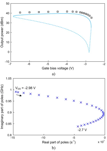
so dc solutions were physically obtained in the whole bias voltage range going from −8 V to −2.3 V. Despite this fact, a free-running oscillation coexists with each dc solution, which in measurements could only be observed by injecting input power up to a certain level and then decreasing this power to zero. The described situation prevents the detection of this oscillation when performing a stability analysis of the dc solution. As an example, Fig. 12(a) presents the closed oscillation curve obtained for Cin = 18 pF versus VGS. The
oscillation amplitude does not decay to zero for any VGS value,
so there are no Hopf bifurcations in dc regime. This is why this oscillation does not start-up from the noise level. Arguably, the oscillation in Fig. 9(b) should arise at a Hopf bifurcation from dc regime, obtained versus the gate bias voltage for some combinations of the capacitor Cin and other circuit element
values. Fig. 12(b) presents the variation of the dominant poles of the dc solution versus the gate bias voltage. The poles approach the imaginary axis but do not cross this axis, which prevents the detection of the coexisting high amplitude oscillation of the PA. As already stated, to obtain this oscillation in measurements it was necessary to inject the circuit with enough input power from the driving source and then reduce Pin to zero for a particular value of VGS. Once
oscillating, VGS can be varied to obtain the measurement
points. The measurement points obtained in this way are superimposed in Fig. 12(a). The reason why the input power is able to start the oscillation will be understood after a thorough stability analysis of the periodic solution curves obtained versus the input power.
The impact of the free-running oscillation in Fig. 12(a) on the stability properties of the PA power-transfer curves will be analyzed considering variations in the capacitor Cin, which
directly affects the input matching and oscillation conditions, as gathered from Fig. 9. This capacitor will be varied from 12 pF to 23 pF. Fig. 13 presents the turning point and Hopf bifurcation loci, calculated with (7) and (9), respectively, in
the plane defined by the input power and the capacitance Cin.
The Cin values (starting at Cin0 = 15.8 pF) that give rise to a
free-running oscillation, as detected from the solution curve in Fig. 9(b), are indicated with a thick vertical line at Pin = 0 W.
For these capacitor values when increasing Pin from zero, the
oscillation associated will give rise to a self-oscillating mixing regime coexisting with the periodic stable solution. This quasi-periodic regime has never been observed experimentally when increasing the input power from zero. Once the circuit is operating in the upper section of a given periodic solution curve, it is observed when reducing the input power. Then, there is a transition from a periodic regime at fin to a
self-oscillating mixer solution. This solution is mathematically extinguished at certain input power, so it only exists in the lower input power range. Depending on the input frequency value, it can be extinguished in two different manners: through synchronization or through an inverse Hopf bifurcation.
-7 -6 -5 -4 -3 -2 -10 0 10 20 30 40 50
Gate bias voltage (V)
Output power (dBm ) a) -15 -10 -5 0 x 107 0.8 0.85 0.9 0.95 1 1.05
Real part of poles (s-1)
Imaginary part of poles
(GHz
)
VGS = -2.98 V
-2.7 V
b)
Fig. 12. (a) Output power versus gate bias voltage for Cin = 18 pF in
free-running operation. Stable (unstable) sections are in solid (dashed) line. Square symbols are measurements. (b) Stability analysis of the dc solution versus the gate bias voltage.
Synchronization will occur for capacitor values such that the free-running oscillation frequency is close enough to the frequency of the input generator fin. Because of the similarity
of the two frequencies, the input source will have a significant influence over the self-oscillation. Therefore, the synchronization will take place for rather low input power
values. Inverse Hopf bifurcations will be obtained for capacitor values such that the free-running oscillation frequency is farther away from fin. Because of the larger
frequency difference, a higher input power will be required for extinction of the oscillation. As described in the following, the parameter region for the occurrence of each of the two phenomena is easily determined from inspection of Fig. 13.
0 2 4 6 8 10 12 14 11 16 21 26 Input power (mW)
Input matching capacitor
(pF ) 30 Os CT CT Section 1 Section 2 12 pF Cin0 13 pF 16 pF 23 pF
Fig. 13. Turning point (solid line) and Hopf bifurcation (dashdot line) loci represented in the plane defined by Pin and Cin. The capacitor values giving
rise to a free-running oscillation have been marked with a thick solid line. The Cin values analyzed in Fig. 14 are marked.
As already stated, a stable free-running oscillation will exist for all the capacitor values in the thick solid line in Fig. 13. In the neighborhood of the degenerate point Os, the transition to
periodic regime will take place when crossing the turning point locus as the input power is increased. In fact, turning points do not always indicate jump phenomena, but may also correspond to synchronization (limit cycle on a saddle-node in the Poincaré map), as described in [6,12].
As a general rule, turning points near the free-running oscillation, having no Hopf bifurcations in the neighborhood, will correspond to synchronization [5]. In the diagram of Fig. 13, this will be the case for Cin values between 15.8 pF and
20.8 pF. Oscillation extinction through an inverse Hopf bifurcation takes place for a higher difference between fin and
the original free-running value. In the diagram of Fig. 13, this occurs when Section 2 of the Hopf bifurcation locus is crossed when increasing the input power. This is the case for capacitor values Cin > 20.8 pF. It is important to emphasize that the
free-running oscillation in Fig. 13 cannot be detected with a small-signal stability analysis.
Section 1 of the Hopf locus corresponds to Hopf bifurcations in the lower section of the multivalued curves. Their implications on the circuit solution will be better understood when superimposing the Hopf bifurcation locus on the power-transfer curves obtained for different Cin values.
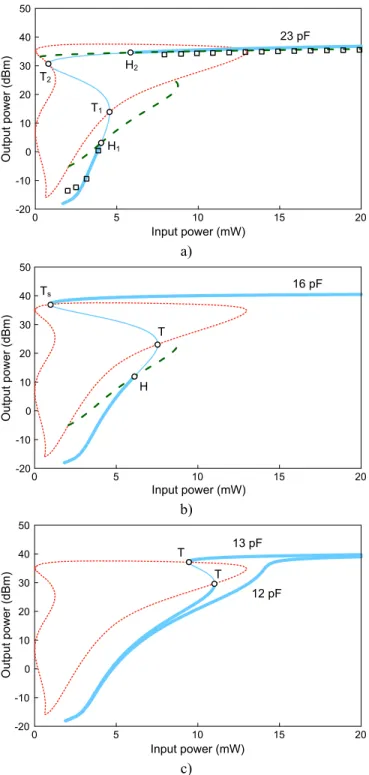
Fig. 14(a-b) presents the power-transfer curves obtained for
Cin = 23 pF and Cin = 16 pF, respectively. The turning point
locus obtained with (7) passes through all the infinite-slope points of the solution curves (marked in the figure with T), as can be verified through simple inspection. On the other hand, the Hopf locus obtained with (9) passes through all the Hopf
bifurcaton points (marked with H), as will be validated later with pole-zero identification.
0 5 10 15 20 -20 -10 0 10 20 30 40 50 Input power (mW) Output power (dBm ) H1 H2 23 pF T1 T2 a) 0 5 10 15 20 -20 -10 0 10 20 30 40 50 Input power (mW) Output power (dBm ) Ts 16 pF H T b) 0 5 10 15 20 -20 -10 0 10 20 30 40 50 Input power (mW) Output power (dBm ) T T 13 pF 12 pF c)
Fig. 14. Periodic solution curves of the PA: output power versus input power for different values of Cin. The stable sections are highlighted. The turning
point (dashed line) and Hopf bifurcation (dashdot line) loci, together with the bifurcations points, have been included. (a) Cin = 23 pF. Square symbols are
measurements. (b) Cin = 16 pF. (c) Cin = 13 pF and 12 pF.
The case of Cin = 23 pF will be initially considered. The
lower section of the power-transfer curve, up to the point H1, is stable. This is because, when injecting the input power, it emerges from a stable dc regime. At the Hopf bifurcation, a quasi-periodic regime is generated, which should be extinguished from certain input power, due to the natural
reduction of the negative resistance with the input amplitude. When the oscillation is extinguished, a jump takes place to the upper section of the periodic curve, with stable behavior. Now, reducing the input power, the circuit remains in the stable periodic solution up to the Hopf bifurcation H2, where an oscillation is generated. Note that when increasing the input power from zero, the self-oscillation [due to the existence of free-running solutions in Fig. 9(b)] is extinguished at this same bifurcation. However, because of the coexistence of the stable periodic solution with this oscillatory regime, it will be rare to observe this oscillation when increasing the input power from zero. The upper section of the periodic curve is unstable between the turning point and the Hopf bifurcation, so the potential jump point T2 is never reached physically.
In the case of Cin = 16 pF, when increasing Pin from zero,
the periodic solution curve will be stable up to the Hopf bifurcation point H. In a manner similar to the previous case, a transition to quasi-periodic regime will occur at this point and then to the upper section of the periodic curve, with stable behavior. When decreasing the input power, the upper section of the curve keeps stable up to the turning point TS, which is, in fact, a synchronization point. The reason for the different behavior is that the input frequency 0.9 GHz is quite close to the free-running oscillation frequency obtained for Cin = 16 pF,
so the transition to quasi-periodic regime is through a loss of synchronization.
For Cin = 13 pF, there is no longer a free-running oscillation,
as gathered from Fig. 9(b), so, as can be expected, there is no Hopf bifurcation in the lower section of the periodic solution curve in Fig. 14(c), in agreement with Fig. 13. The two turning points will give rise to jumps between different sections of the multivalued periodic curve (hysteresis). For Cin = 12 pF, a
regular curve showing gain expansion, with neither oscillation nor jumps, is obtained.
As gathered from the bifurcation loci in Fig. 13, there can be Hopf bifurcations in the lower section of the curves (Section 1 of the Hopf bifurcation locus) even when there are no free-running oscillations. The quasi-periodic regime generated at these points should exhibit a turning point when increasing the input power (as those reported in [5,11]) and be extinguished in a saddle-connection bifurcation in the Poincaré map [12]. This is a global bifurcation [12] that requires the presence of a saddle point, such as those in the intermediate section of the multivalued solution curves. The saddle-connection bifurcation is also associated with co-dimension two bifurcations, at which the turning point and the Hopf bifurcation loci merge, such as the ones indicated with CT in Figs. 9(a), 13.
The accuracy of the Hopf bifurcation detection has been validated with pole-zero identification. Fig. 15 shows the evolution of the critical poles of the solution curve corresponding to Cin = 23 pF. The pole locus indicates that the
lower section is stable up to Pout = 4 dBm, where the poles
cross to the right-hand side of the complex plane (RHP), giving rise to a Hopf bifurcation from periodic regime. The
poles merge and split into two real poles, and for
Pout = 14.7 dBm one of the real poles crosses to the left-hand side of the complex plane (LHP) at a turning point in the solution curve. This real pole crosses again to the RHP at
Pout = 30.9 dBm giving rise to the second turning point in the solution curve. When further increasing the input power, the two real poles merge on the RHP and split into two pairs of complex-conjugate poles (associated with a same pair of Floquet multipliers [5-6,36]). At Pout = 34.6 dBm, the poles
cross to the LHP giving rise to an inverse Hopf bifurcation from which the periodic solution curve becomes stable. The pole analysis is in total agreement with the results of the bifurcation analysis in Fig. 13 and Fig. 14(a).
-2 -1 0 1 2 3 4 x 10⁸ 0.75 0.8 0.85 0.9 0.95 1 1.05
Real part of poles (s-1)
Imaginary part of poles
(GHz ) Pout = -16.5 dBm 4 dBm 30.9 dBm 14.7 dBm 34.6 dBm 34.6 dBm Pout = -16.5 dBm 4 dBm
Fig. 15. Pole locus of the solution curve in Fig. 14(a) obtained for Cin = 23 pF.
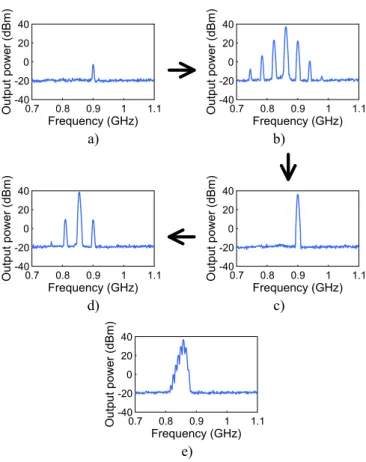
The PA measurements for an input matching capacitor of 12 pF have been superimposed in Fig. 14(a). The capacitor value is significantly lower in measurements that the one used in simulations. As mention in Subsection II-A, the capacitor value that best matched the input of the PA in measurements was already lower than the one used in simulations. The shift in the capacitor value is attributed to modeling inaccuracies. One must take into account also that the Cin value used in the
simulations was a combination of a lower capacitor value and an ideal capacitor connected in parallel, to be able to vary the capacitance continuously, as explained in Subsection III-A. Even under this unavoidable accuracy limitations, the qualitative behavior and power levels are reproduced satisfactory. The measured spectra at different input power values are shown in Fig. 16. At low input power, the spectrum is periodic, as shown in Fig. 16(a). When continuously increasing the input power, a Hopf bifurcation is obtained at
Pin = 6.8 dBm, which gives rise to the quasi-periodic spectrum in Fig. 16(b). When further increasing the input power, the self-oscillation vanishes due to a turning point in the quasi-periodic solution curve, so a jump takes place at Pin = 8.6 dBm
to the upper section of the periodic solution curve. Fig. 16(c) shows the spectrum obtained for Pin = 14.7 dBm. Now, when
reducing the input power, the PA keeps behaving in periodic regime up to the input power Pin = 8 dBm, at which the circuit
undergoes a Hopf bifurcation. Below Pin = 8 dBm, the circuit
operates in a quasi-periodic regime [Fig. 16(d)] that is never observed when increasing the input power from zero. The results are in total agreement with the two Hopf bifurcation points that were detected with (9) and displayed in Fig. 13 and Fig. 14(a).
With the discrete capacitor values available during the experimental tests it was not possible to observe a synchronization phenomenon with the input frequency
fin = 0.9 GHz. This is because for those capacitor values the frequency of the free-running oscillation that coexists with the dc solution is too different from fin = 0.9 GHz. To validate the
existence of the phenomenon, a small shift was applied to the input frequency, using, instead, the value fin = 0.866 GHz,
together with the capacitor Cin = 12 pF. With these parameter
values, synchronization could be measured. The typical near-synchronization spectrum, with a triangular shape [37], is shown in Fig. 16(e).
0.7 0.8 0.9 1 1.1 -40 -20 0 20 40 Frequency (GHz) Output power (dBm ) 0.7 0.8 0.9 1 1.1 -40 -20 0 20 40 Frequency (GHz) Output power (dBm ) 0.7 0.8 0.9 1 1.1 -40 -20 0 20 40 Frequency (GHz) Output power (dBm ) 0.7 0.8 0.9 1 1.1 -40 -20 0 20 40 Frequency (GHz) Output power (dBm ) 0.7 0.8 0.9 1 1.1 -40 -20 0 20 40 Frequency (GHz) Output power (dBm ) a) b) d) c) e)
Fig. 16. Sequence of output spectra measured for Cin = 12 pF. (a) When
increasing the input power from very low value it is periodic (Pin = 5.9 dBm).
(b) Jump to a quasi-periodic solution (Pin = 7.5 dBm). (c) Jump to the
periodic solution (Pin = 14.7 dBm). (d) Now, when decreasing the input
power a quasi-periodic solution, resulting of the mixing with the free-running oscillation, is observed (Pin = −5.1 dBm). Synchronization with this last one
is obtained reducing the input frequency. (e) Adler spectrum near synchronization (fin = 0.866 GHz).
As previously shown, the input power is able to start an oscillation in the PA which persists when reducing the power to zero, even when the dc solution is stable in the whole range considered. In the next subsection, the above study will allow turning the PA into a highly efficient free-running power oscillator.
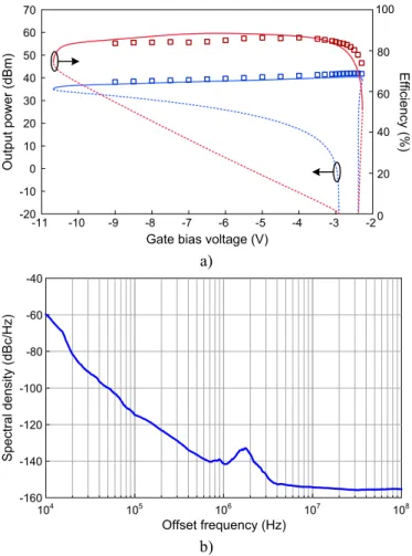
A. High efficiency RF Class-E power oscillator
In simulation, a shift of the pole locus in Fig. 12(b) to the right is observed when suppressing the 50-Ohm load of the input source. This gives rise to an interval of VGS values for
which the dc solution becomes unstable, allowing the oscillation to start-up from the noise level. Fig. 17(a) presents the free-running oscillation curve obtained for the original capacitor value Cin = 13 pF in the design of Fig. 1(a). Note that
the oscillation persists in a large gate bias voltage interval. The Hopf bifurcation from dc regime is subcritical [5,12,38], so the oscillation amplitude grows for decreasing values of VGS. In
measurements, the value of VGS for which the oscillation starts
up (−2.8 V) agrees with the Hopf bifurcation point obtained in simulation. The evolution observed versus VGS is in total
agreement with the predicted results.
-11 -10 -9 -8 -7 -6 -5 -4 -3 -2 -20 -10 0 10 20 30 40 50 60 70
Gate bias voltage (V)
Output power (dBm ) 100 80 60 40 20 0 Efficiency (%) a) 104 105 106 107 108 -160 -140 -120 -100 -80 -60 -40 Offset frequency (Hz) Spectral density (dBc /Hz ) b)
Fig. 17. (a) Output power and efficiency of the RF Class-E power oscillator, represented versus the gate bias voltage. Square symbols are measurements. (b) Phase noise spectral density measured at VGS = −3.3 V.
In comparison with other configurations, requiring an accurate synthesis of a feedback network [38], the oscillator topology is greatly simplified. Indeed, the feedback path is here provided by the device gate-to-drain capacitance (CGD).
In Fig. 17(a), the efficiency variation has also been represented versus the gate bias voltage. A peak value as high as 86.4% was measured for VGS = −4 V, staying above 80% for VGS ≤ −2.5 V. The gate bias voltage provides a simple way to
control the oscillation frequency. For the voltage interval considered in Fig. 17(a), it varies between 0.826 GHz and 0.98 GHz.
Finally, the phase noise spectral density was captured for several oscillation frequencies and no noticeable difference was appreciated. In Fig. 17(b), it is represented at
VGS = −3.3 V. Phase noise values of −114.8 dBc/Hz and −141.4 dBc/Hz were estimated for frequency offsets of 100 kHz and 1 MHz, respectively, in the ranges reported in the literature for GaN HEMT based oscillators [39].
V. CONCLUSION
An in-depth investigation of hysteresis in a Class-E power amplifier has been presented, demonstrating that it is due to a nonlinear resonance of the transistor input capacitance with the inductive input matching network. The different set of circuit parameters and operating conditions that give rise to turning points in the solution curves are efficiently detected with an outer-tier method, under a geometrical condition for infinite slope. Under an increase of the drain bias voltage, the locus evolves so as to give rise to a free-running oscillation that for the most usual circuit element values cannot be detected with any standard stability analysis, even under an exhaustive variation of the bias voltages. Under input power injection, this oscillation will give rise to an undesired self-oscillating mixer regime, extinguished either through synchronization or inverse Hopf bifurcations. The Hopf bifurcations in the multivalued curves can be efficiently detected combining the outer-tier method with a limit-oscillation condition imposed with the aid of a small-signal auxiliary generator. The great flexibility in the bifurcation analysis has enabled a thorough investigation of the circuit stability properties under extensive variations of bias voltages, input power and circuit element values. In this way, it has been possible to modify the original PA design, close to the state-of-the-art for the UHF band, so as to make a practical use of the oscillation originally associated with the degenerated turning points. It has been possible to obtain a high efficiency Class-E oscillator with a slight variation of the input network, providing 154 MHz of frequency coverage with an efficiency figure above 80%.
ACKNOWLEDGMENT
The authors would like to thank M.N. Ruiz, University of Cantabria, for her assistance with measurements, J.Mª. Salmón (retired) for kindly crafting the aluminum carriers for the PA, S. Pana, University of Cantabria, for her help with the fabrication of the prototype and R. Baker, Cree Inc., for the support provided.
REFERENCES
[1] F.H. Raab, P. Asbeck, S. Cripps, P.B. Kenington, Z.B. Popovic, N. Pothecary, J.F. Sevic, and N.O. Sokal, “Power amplifiers and transmitters for RF and microwave,” IEEE Trans. Microw. Theory Techn., vol. 50, no. 3, pp. 814–826, Mar. 2002.
[2] Jeon, A. Suárez, and D.B. Rutledge, “Analysis and elimination of hysteresis and noisy precursors in power amplifiers,” IEEE Trans. Microw. Theory Techn., vol. 54, no. 3, pp. 1096–1106, Mar. 2006. [3] J. de Cos, A. Suárez, and J.A. García, “Parametric hysteresis in power
amplifiers,” IEEE MTT-S Int. Microwave Symp. Dig., 2015, pp. 1–4. [4] N.-Ch. Kuo, P.-S. Chi, A. Suárez, J.-L. Kuo, P.-Ch. Huang, Z.-M. Tsai,
and H. Wang, “DC/RF Hysteresis in Microwave pHEMT Amplifier Induced by Gate Current—Diagnosis and Elimination,” IEEE Trans. Microw. Theory Techn., vol. 59, no. 11, pp. 2919–2930, Nov. 2011. [5] A. Suárez, Analysis and Design of Autonomous Microwave Circuits.
Hoboken, New Jersey: John Wiley & Sons, 2009.
[6] T. S. Parker and L. O. Chua, Practical Numerical Algorithms for Chaotic Systems. New York: Springer-Verlag, 1989.
[7] E. Palazuelos, A. Suárez, J. Portilla, and F.J. Barahona, “Hysteresis prediction in autonomous microwave circuits using commercial software: application to a Ku-band MMIC VCO,” IEEE J. Solid-State Circuits, vol. 33, no. 8, pp. 1239–1243, Aug. 1998.
[8] J. de Cos and A. Suárez, “Efficient simulation of solution curves and bifurcation loci in injection-locked oscillators,” IEEE Trans. Microw. Theory Techn., vol. 63, no. 1, pp. 181–197, Jan. 2015.
[9] D. Hente and R. H. Jansen, “Frequency-domain continuation method for the analysis and stability investigation of nonlinear microwave circuits,” IEE Proc., vol. 133, pt. H , no. 5, pp. 351–362, Oct. 1986.
[10] L. O. Chua and A. Ushida, “A switching-parameter algorithm for finding multiple solutions of nonlinear resistive circuits,” Int. J. Circuit Theory Applicat., vol. 4, no. 3, pp. 215–239, Jul. 1976.
[11] A. Suárez, J. Morales, and R. Quéré, “Synchronization analysis of autonomous microwave circuits using new global-stability analysis tools,” IEEE Trans. Microw. Theory Techn., vol. 46, no. 5, pp. 494– 504, May 1998.
[12] J. Guckenheimer and P. Holmes, Nonlinear Oscillations, Dynamic Systems, and Bifurcations of Vector Fields. New York: Springer-Verlag, 1983.
[13] S. Wiggins, Introduction to Applied Nonlinear Dynamical Systems and Chaos. New York: Springer-Verlag, 1990.
[14] J. Ebert and M. Kazimierczuk, “Class E high-efficiency tuned power oscillator,” IEEE J. Solid-State Circuits, vol. 16, no. 2, pp. 62–66, Apr. 1981.
[15] H. Hase, H. Sekiya, J. Lu, and T. Yahagi, “Resonant DC/DC converter with class E oscillator,” IEEE Int. Symp. Circuits Syst., 2005, pp. 720– 723.
[16] A.N. Laskovski and M.R. Yuce, “Class-E oscillators as wireless power transmitters for biomedical implants,” in Int. Symp. Applied Sciences Biomed. Comm. Tech., 2010, pp. 1–5.
[17] F.H. Raab, “Idealized operation of the class E tuned power amplifier,” IEEE Trans. Circuits Syst., vol. 24, no. 12, pp. 725–735, Dec. 1977. [18] F. H. Raab, "Class-E, Class-C, and Class-F power amplifiers based upon
a finite number of harmonics," IEEE Trans. Microw. Theory Techn., vol. 49, no.8, pp.1462-1468, Aug 2001.
[19] J.A. García, R. Marante, and M.N. Ruiz, “GaN HEMT Class E2 Resonant Topologies for UHF DC/DC Power Conversion,” IEEE Trans. Microw. Theory Techn., vol. 60, no. 12, pp. 4220–4229, Dec. 2012. [20] R. Negra and W. Bächtold, “Lumped-element load-network design for
class-E power amplifiers,” IEEE Trans. Microw. Theory Techn., vol. 54, no. 6, pp. 2684–2690, Jun. 2006.
[21] N.O. Sokal and A. Mediano, “Redefining the optimum RF Class-E switch-voltage waveform, to correct a long-used incorrect waveform,” IEEE MTT-S Int. Microwave Symp. Dig., 2013, pp. 1–3.
[22] N. D. Lopez, J. Hoversten, M. Poulton, and Z. Popovic, “A 65-W high-efficiency UHF GaN power amplifier,” IEEE MTT-S Int. Microwave Symp. Dig., 2008, pp. 65–68.
[23] J. Cumana, A. Grebennikov, G. Sun; N. Kumar, and R.H. Jansen, “An Extended Topology of Parallel-Circuit Class-E Power Amplifier to Account for Larger Output Capacitances,” IEEE Trans. Microw. Theory Techn., vol. 59, no. 12, pp. 3174–3183, Dec. 2011.
[24] A. Al Tanany, A. Sayed, and G. Boeck, “Broadband GaN switch mode class E power amplifier for UHF applications,” IEEE MTT-S Int. Microwave Symp. Dig., 2009, pp. 761–764.
[25] T.B. Mader, E.W. Bryerton, M. Markovic, M. Forman, and Z. Popovic, “Switched-mode high-efficiency microwave power amplifiers in a free-space power-combiner array,” IEEE Trans. Microw. Theory Techn., vol. 46, no. 10, pp. 1391–1398, Oct. 1998.
[26] Y.Qin, S. Gao, P. Butterworth, E. Korolkiewicz, and A. Sambell, “Improved design technique of a broadband class-E power amplifier at 2GHz,” in Europ. Microwave Conf., 2005, pp. 4–6.
[27] H.G. Bae, R. Negra, S. Boumaiza, and F.M. Ghannouchi, “High-efficiency GaN class-E power amplifier with compact harmonic-suppression network,” in Europ. Microwave Conf., 2007, pp. 9–12. [28] M.P. van der Heijden, M. Acar, and J.S. Vromans, “A compact 12-watt
high-efficiency 2.1-2.7 GHz class-E GaN HEMT power amplifier for base stations,” IEEE MTT-S Int. Microwave Symp. Dig., 2009, pp. 657– 660.
[29] L. C. Nunes, P.M. Cabral, and J.C.Pedro, “AM/AM and AM/PM Distortion Generation Mechanisms in Si LDMOS and GaN HEMT Based RF Power Amplifiers,” IEEE Trans. Microw. Theory Techn., vol. 62, no. 4, pp. 799–809, Apr. 2014.
[30] A. Suárez and R. Quéré, Stability Analysis of Nonlinear Microwave Circuits. Boston, MA: Artech House, 2003.
[31] J. Jugo, J. Portilla, A. Anakabe, A. Suárez, and J. M. Collantes, “Closed-loop stability analysis of microwave amplifiers,” Electron. Lett., vol. 37, no. 4, pp. 226–228, Mar. 2001.
[32] N. Ayllon, J.M. Collantes, A. Anakabe, I. Lizarraga, G. Soubercaze-Pun, and S. Forestier, “Systematic Approach to the Stabilization of Multitransistor Circuits,” IEEE Trans. Microw. Theory Techn., vol. 59, no. 8, pp. 2073–2082, Aug. 2011.
[33] S. Jeon, A. Suárez, and D.B. Rutledge, “Global stability analysis and stabilization of a class-E/F amplifier with a distributed active transformer,” IEEE Trans. Microw. Theory Techn., vol. 53, no. 12, pp. 3712–3722, Dec. 2005.
[34] J. M. Paillot, J. C. Nallatamby, M. Hessane, R. Quéré, M. Prigent, and J. Rousset, “A general program for steady state, stability, and FM noise analysis of microwave oscillators,” IEEE MTT-S Int. Microwave Symp. Dig., 1990, pp. 1287–1290.
[35] V. Rizzoli, F. Mastri, and D. Masotti, “General noise analysis of nonlinear microwave circuits by the piecewise harmonic-balance technique,” IEEE Trans. Microw. Theory Techn., vol. 42, no. 5, pp. 807–819, May 1994.
[36] J. M. Collantes, I. Lizarraga, A. Anakabe, and J. Jugo, “Stability verification of microwave circuits through Floquet multiplier analysis,” in Proc. IEEE Asia–Pacific Circuits Syst., 2004, pp. 997–1000. [37] R. Adler, “A study of locking phenomena in oscillators,” Proc. IEEE,
vol. 61, no. 10, pp. 1380–1385, Oct. 1973.
[38] S. Jeon, A. Suárez, and D.B. Rutledge, “Nonlinear design technique for high-power switching-mode oscillators,” IEEE Trans. Microw. Theory Techn., vol. 54, no. 10, pp. 3630–3640, Oct. 2006.
[39] M. Horberg, L. Szhau, T. N. T. Do, and D. Kuylenstierna, “Phase noise analysis of a tuned-input/tuned-output oscillator based on a GaN HEMT device,” in Europ. Microwave Conf., 2014, pp. 1118–1121.
Jesús de Cos (S’15) was born in Santander, Spain.
He received the Telecommunications Engineering degree and the MsC degree from the University of Cantabria, Santander, Spain, in 2010 and 2011, respectively. He is currently working towards his Ph.D. degree at the University of Cantabria. His research interests include stability analysis, bifurcation theory and circuit simulation techniques applied to microwave circuits.
Mr. de Cos was a finalist in the International Microwave Symposium Student Paper Competition in 2015.
Almudena Suárez (M’96–SM’01–F’12) was born
in Santander, Spain. She received the Electronic Physics degree and Ph.D. degree from the University of Cantabria, Santander, Spain, in 1987 and 1992, respectively, and the Ph.D. degree in electronics from the University of Limoges, Limoges, France, in 1993.
She is currently a Full Professor with the Communications Engineering Department,
University of Cantabria. She coauthored Stability analysis of nonlinear microwave Circuits (Artech House, 2003) and authored Analysis and design of autonomous microwave circuits (IEEE-Wiley, 2009).
She is a member of the Technical Committees of the International Microwave Symposium (IMS) and the European Microwave Conference. She was an IEEE Distinguished Microwave Lecturer during the period 2006– 2008. She has been a member of the board of directors of the European Microwave Association (EuMA) since 2012 and is the Editor in Chief of International Journal of Microwave and Wireless Technologies.
José A. García (S’98–A’00–M’02) was born in
Havana, Cuba. He received the Telecommunications Engineering degree from the Instituto Superior Politécnico “José A. Echeverría” (ISPJAE), Havana, Cuba, in 1988, and the Ph.D. degree from the University of Cantabria, Santander, Spain, in 2000. From 1988 to 1991, he was a Radio System Engineer with a high-frequency (HF) communication center, where he designed antennas and HF circuits. From 1991 to 1995, he was an Instructor Professor with the Telecommunication Engineering Department, ISPJAE. From 1999 to 2000, he was with Thaumat Global Technology Systems, as a Radio Design Engineer involved with base-station arrays. From 2000 to 2001, he was a Microwave Design Engineer/Project Manager with TTI Norte, during which time he was in charge of the research line on SDR while involved with active antennas. From 2002 to 2005, he was a Senior Research Scientist with the University of Cantabria, where he is currently an Associate Professor. During 2011, he was a Visiting Researcher with the Microwave and RF Research Group, University of Colorado at Boulder. His main research interests include nonlinear characterization and modeling of active devices, as well as the design of power RF/microwave amplifiers, wireless powering rectifiers and RF dc/dc power converters.
![Fig. 1. (a) Schematic of the Class-E power amplifier demonstrator [3]. Values in the table are for Colcraft Air Core inductors and ATC 100B capacitors](https://thumb-us.123doks.com/thumbv2/123dok_es/6873100.287801/3.918.74.449.75.316/schematic-class-amplifier-demonstrator-values-colcraft-inductors-capacitors.webp)