Abstract— A rigorous analysis of noise effects in super regenerative oscillators (SRO), operating in both linear and nonlinear mode, is presented. For operation in linear mode, two different analysis methods are presented. One is based on the calculation of linear-time variant (LTV) transfer function with respect to the input signal and the noise sources. The second method is based on a compact semi-analytical formulation of the pulsed oscillator under the effect of the quench signal. The compact formulation also enables the analysis of the SRO in nonlinear mode. It constitutes a fully new mathematical description of SROs, with general applicability, as it is not restricted to a particular oscillator topology. It relies on a numerical nonlinear black-box model of the standalone free-running oscillator, extracted from harmonic-balance simulations. This model is introduced into an envelope-domain formulation of the SRO at the fundamental frequency. Both the method based on LTV transfer functions and the semi-analytical formulation take into account the cyclostationary nature of the SRO response to the noise sources. In nonlinear mode, the variances of the amplitude and phase are calculated linearizing the formulation about the pulsed steady-state solution. The particular time variation of the phase variance is explained in detail, and related with the onset and extinction of the oscillation in the presence of an RF input signal. The new analysis methods have been validated with both independent circuit-level simulations and measurements.
Index Terms—Noise, stability, superregenerative oscillator. I. INTRODUCTION
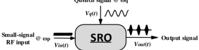
Superregenerative oscillators (SROs) use the exponential growth of an oscillation signal to obtain high gain amplification, which has been applied to replace amplifier chains in receivers [1], [2] and, more recently, to implement active transponders [3], [4]. The oscillation is controlled by a quench signal (Fig. 1) that periodically switches the oscillator on and off, by shifting the critical pair of complex-conjugate poles from the left-hand side of the complex plane (LHS) to the right-hand side (RHS) and then back to the LHS. The SRO is sensitive to the input signal only during a fraction of the quench-signal period, about the time value at which the critical pair of complex-conjugate poles crosses to the RHS. The signal grows as long as this critical pair of poles is located on the RHS, so the maximum value of the output signal is obtained when the poles cross again to the LHS [1], [2]. Thus, the SRO responds
This paper is an expanded version from the IEEE MTT-S International Microwave Symposium (IMS 2019), Boston, MA, USA, June 2-7, 2019. This work was supported by the Spanish Ministry of Economy and Competitiveness and the European Regional Development Fund (ERDF/FEDER) under the research project TEC2017-88242-C3-1-R.
with an oscillation pulse, controlled by the quench signal, Vq(t). In the absence of an input signal, the oscillation starts from the noise level, whereas in the presence of an RF input signal (above the noise level) it starts from a higher amplitude. In fact, when operating in linear mode, the amplitude of the oscillation pulse is proportional to that of the input signal, as shown in [1]. On the other hand, when operating in nonlinear mode, the active device or devices are sensitive to the oscillation amplitude, and may reach a saturated value [1],[5],[6]. In the so-called logarithmic mode, the area under the envelope of the oscillation pulse is proportional to the input-signal amplitude.
Fig. 1. Schematic representation of the SRO operation.
Under an amplitude modulation, the SRO should operate in linear mode, and each oscillation pulse must depend only on the RF signal Vin(t) introduced during its corresponding sensitivity period, avoiding hangover effects [1]. However, the SRO also responds to noise perturbations, which under the commonly used on-off keying modulation [1], [5], may give rise to detectable output pulses in the absence of an input signal. Thus, for a proper operation, a sufficiently high signal-to-noise ratio (S/N) is necessary. On the other hand, SROs can also operate under phase and frequency modulations [7]-[10]. For instance, very performant QPSK receivers have been presented in [7], [11], where the symbol rate agrees with the quench-signal frequency. As shown in [7], the SRO can follow the variations of the input phase in both linear and nonlinear mode, and the nonlinear one enables a broader choice of quench-signal parameters. In nonlinear mode, one can expect the inherent oscillation noise to have an impact on the output pulses. The dominant contribution is the phase noise, due to the invariance of the oscillator solution versus phase translations, which, in the presence of noise sources, gives rise to an accumulation of phase perturbations [12],[13].
Most of the previous works [14], [15] on SRO noise analysis consider a simplified Van der Pol model of the oscillator circuit
The authors are with Dpto. Ingeniería de Comunicaciones, Universidad de Cantabria., Av. Los Castros 39005, Santander, Spain (e-mail: [email protected], [email protected], [email protected]).
SRO
Quench signal @ ωq
Small-signal
RF input @ ωp Output signal
Vq(t)
Vin(t) Vout(t)
Noise Analysis of Superregenerative
Oscillators in Linear and Nonlinear Modes
Sergio Sancho, Member, IEEE, Silvia Hernández, Student Member, IEEE, Almudena Suárez, Fellow, IEEE
and focus on the S/N calculation in linear regime. The aim of this work is to present a generic noise analysis of SROs in both linear and nonlinear modes. In [16], the analysis in linear mode was carried out using linear-time-variant (LTV) transfer functions [17], [18] directly extracted from circuit-level envelope-transient simulations [19], [20]. However, it is not possible to extend this kind of representation to nonlinear mode. In [6], a single time-variant Volterra kernel in the envelope domain [21] was defined, but this nonlinear model is only applicable when the input-amplitude levels are known and a proper timing of the input-amplitude variations is used.
To cover the noise analysis in both linear and nonlinear mode, a second method is presented, based on a compact semi-analytical formulation of the pulsed oscillator under the effect of the quench signal. It relies on a numerical nonlinear black-box model of the standalone free-running oscillator, extracted from harmonic-balance (HB) simulations and introduced into an envelope-domain formulation of the SRO at the fundamental frequency. The semi-analytical formulation considers the amplitude and phase as state variables, enabling the stochastic analysis of the influence of each of these variables on the global noise behavior.
For RF input amplitudes and quench signals, such that the SRO operates in linear mode, the calculation through the new semi-analytical formulation is equivalent to the one resulting from an LTV transfer function, defined at the analysis port. Although the equation from which the stochastic analysis departs is different when using LTV transfer functions and when using the semi-analytical formulation, the stochastic analysis is analogous in the two cases. It is based on the calculation of the Fourier series expansion of the cyclostationary autocorrelation function, with the quench frequency as fundamental and time-varying harmonic terms. When using the LTV transfer functions, one calculates the autocorrelation of the complex output voltage, whereas in the case of the semi-analytical formulation, one calculates separately the autocorrelation of the amplitude and phase variables to analyze their stochastic properties.
When using the semi-analytical formulation, the variances of the amplitude and phase, in the presence of noise perturbations, will be calculated linearizing the formulation about the pulsed steady-state solution. The particular time variation of the phase variance will be explained in detail, and related with the onset and extinction of the oscillation. The prediction capabilities of formulation will be tested under highly nonlinear behaviour and irregular envelopes
The paper is organized as follows. Section II provides a summary of the method to calculate the signal-to-noise ratio in linear regime, presented in [16], and relying on the use of LTV transfer functions. Section III describes the new reduced-order envelope-domain formulation of the SRO, valid for linear and nonlinear operation. Section IV describes the whole stochastic analysis of the SRO amplitude and phase in the presence of noise sources.
II. NOISE ANALYSIS IN LINEAR MODE BASED ON LTV
TRANSFER FUNCTIONS
The analysis in this section is intended to be applied using linear-time variant (LTV) transfer functions [17], [18],
extracted from circuit-level envelope-transient simulations [19], [20]. The method is applicable only when the SRO operates in linear mode.
A. LTV Transfer Functions with Respect to the Noise Sources The envelope-domain analysis of the SRO is performed, taking the oscillator free-running frequency p 2fp as the
carrier frequency. Then, the SRO output due to noise is expressed as:
( ) ( ) cos ( ) Re ( ) j pt
out out p out out
n t N t t t N t e (1) In turn, the independent noise sources are expressed as
( ) j pt m
N t e , where m = 1 to M, and M is the number of noise sources. These noise sources are assumed white, since, in linear mode, there is no up conversion of low-frequency noise. To calculate the LTV transfer function [17]-[18] with respect to the noise source Nm( )t , this source is replaced with an auxiliary deterministic small-signal source, having the general representation j( p )t
Ge , where the constant envelope G may correspond to either a voltage or current. The LTV transfer function associated to this source is given by [18]:
( , ) ( , ) /
m
p out p
H t V t G (2)
where Vout is the envelope of the output voltage. The above function is calculated sweeping in j( p )t
Ge and performing a circuit-level envelope-transient analysis at each step. The frequency Ω is swept about the free-running frequency of the stand-alone oscillator. The sweep-frequency interval must be wide enough to cover the whole resonance bandwidth, as shown in [18].Because the quench signal is periodic, m( , )
p H t is periodic too, with the same period Tq.
B. Stochastic Analysis of the SRO Output
Let a noise source with the envelope N(t) be considered, where the superscript m has been dropped for notation clarity. The output signal due to this noise source is calculated [18] as:
/ 2 / 2 1 ( ) ( , ) ( ) 2 B j t out p B N t H t N e d
(3)where N( ) Nr( ) jNi( ) . For simplicity, the integration frequency interval about p is assumed to be symmetrical and B is the noise bandwidth. To obtain the power spectral density (PSD) of the process Nout( )t , one must first calculate the correlation function ( , )R t , with a double time dependence. In the case of the white-noise source N(t), this is obtained as:
1 2 1 * / 2 / 2 (( ) ) 1 2 1 2 1 2 / 2 / 2 2 * 1 2 1 2 ( , ) ( ) ( ) ( , ; , ) ( - ) , ( , ; , ) ( , ) ( , ) / 2 out out B B j t H B B H p p R t E N t N t R t e d d R t H t H t
(4)where E N (1) (N 2)* ( 1 2)and is the constant
PSD. Operating the delta function, the above equation simplifies as: 2 / 2 * / 2 1 ( , ) ( , ) ( , ) 2 B j p p B R t H t H t e d
(5)Due to the time periodicity of H t( , p), for each Ω, this
function can be expanded in a Fourier series:
( , ) ( ) jk qt, 2
p k q q
k
H t
H e T (6) Replacing (6) into (5) one obtains [22]:* , ( , ) ( ) ( ) ( ) , ( ) ( ) q js t out out s s s k l k l s R t E N t N t R e R U
(7)where the components Uk l,( ) are given by:
/ 2 ( ) * , 2 / 2 ( ) ( ) ( ) 2 q B j k k l k l B U H H e d
(8)From (7), ( , )R t satisfies:R t( , ) R t( Tq, ) , and, due to the
periodicity of H t( , p), the time average satisfies
out( )
out( q)E N t E N tT . The fulfilment of these two properties indicates that Nout( )t is a cyclostationary stochastic process. Then, as shown in [22], [23], the PSD of this process can be calculated using the term R0( ) of the Fourier series
expansion (7) of the correlation function:
2 0 ( ) ( ) ( ) j out S N R e d
(9)This is because, as demonstrated in [22], [23], only the term with s of summation (7) contributes to the PSD of the 0 cyclostationary process. Comparing (7) and (8), the term R0( )
is:
0 , 2 2 ( ) ( ) ( ), 2 ( ) ( ) q N P jk k k k k N k P j k k R U e g g H e d
(10)where it has been assumed that H for k( ) 0 B/ 2. Introducing (10) in (9), the PSD of the output noise is [16]:
2 2 ( ) ( ) 2 P k q k P S H k
(11)The contribution of each component H is shifted to the k( ) k-th harmonic of the quench frequency . In the case of M q
white-noise sources, with the spectral densities m, where m = 1…M, the analysis should be carried out in the same way as (3)-(11), producing a total output-noise spectral density of
the form , , ( ) m n( ) m n S
S , where , ( ) m nS are the terms arising from the correlation between the m-th and n-th noise sources.
C. Signal to Noise Ratio
The calculation of the signal-to-noise ratio is exemplified considering a single white-noise source with the spectral density . The expression for the noise power is derived using the result (11) for the output noise PSD [11]:
2 2 2 2 ( ) ( ) 2 1 1 ( ) ( ) 2 2 2 out out n H N t n t P R R S d d R R
(12)where (1) has been applied and H2( ) H t( , p)2 is the time average of the square value of the LTV transfer function. On the other hand, the signal power is obtained considering a single RF input tone, which will fulfill
0
( ) ( )
in
V A , where represents a frequency offset 0 from the carrier at . Using the black-box model in [18], the p
signal power is [16]: 2 2 2 0 2 2 0 ( ) 1 = ( , ) 2 2 2 1 ( ) 2 2 i out i s p H V t A P H t R R A R (13) where i( , ) p
H t is the LTV transfer function with respect to the input signal. Finally, the signal-to-noise (S/N) ratio is calculated using (12) and (13) as:
2 2 0 2 ( ) ( ) i H s H A S N P P d
(14)D. Application to a FET-based SRO
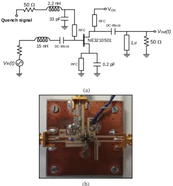
The analysis will be applied to the FET-based SRO of Fig. 2, which is the same circuit considered in [18]. The FET model used in the circuit-level simulations is EE_HEMT1_Model (EEsof Scalable Nonlinear HEMT Model). The drain to source bias voltage is VDS = 0.7 V. The quench signal is η(t) = VGS(t) = Vdc + Vpcos(ωqt), with Vdc = ‒1.583 V, Vp = 1.06 V, and quench-signal frequency fq = 8 MHz. The oscillation frequency fp =2.7 GHz. In small-signal conditions, the drain current consumption is ID = 64 mA. The main white-noise contributions are due to the input 50 Ohm resistor, modeled with a voltage source N1, and the transistor noise,
modelled with an equivalent drain-to-source current source N2.
Thus, the number of noise sources is M = 2. The PSD of the input noise source is 1 = 8.10-19 V2/Hz and that of the transistor
current source, fitted experimentally, is 2 = 4.10-20 A2/Hz. Two
envelope-domain LTV transfer functions m( , ) p
H t , where m = 1, 2, are calculated with respect to these two noise
sources. Fig. 3(a) presents the Fourier components 2 ( ) k
H ,
where k = 0, 1, 2, of the transfer function with respect to the drain noise source, which is the dominant contribution. The PSD of the output noise due to N2 has been calculated through
(11) with P = 32 components, with the result of Fig. 3(b). To illustrate, Fig. 4 presents output voltage paths obtained in simulation and measurements, in the absence of an input signal. It shows the capability of noise perturbations to start low-amplitude oscillation pulses and enables a comparison of the variation ranges and amplitude levels. Fig. 4(a) shows the envelope-transient simulation performed during a time interval of 12 s. It exhibits oscillation pulses of small amplitude, arising from the noise perturbations in the SRO sensitivity interval. This simulation has been used to obtain Nout( )t 2 . Fig. 4(b) presents the experimental measurements during a time interval of 12 s.
To illustrate the calculation of S/N, an input signal of power Pin = -60 dBm and frequency offset 0 ≈ 0 is considered. The
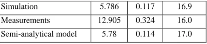
values of P, Ps and S/N obtained using (12)-(14) are shown in Table I. In both circuit-level envelope-transient simulations and measurements, the signal-to-noise ratio is calculated as
2 2
( ) ( )
out out
S N V t N t . In Table I, the results are successfully compared with the predictions of the new method.
Fig. 2. Schematic and photograph of the FET-based SRO. The frequencies of the oscillation and quench signals are fp = 2.7 GHz and fq = 8 MHz, respectively.
(a)
(b)
Fig. 3. Calculation of the output noise PSD. (a) Fourier coefficients H k( ) of ( , p)
H t , for k = 0, 3, 5. (b) PSD of the output signal due to a white-noise current source N2. The PSD of the source is 2 = 4.10-20 A2/Hz.
Fig. 4. Output voltage paths in the presence of noise perturbations only. (a) Envelope-transient simulation. (b) Measurements.
Table I. Signal to noise ratio calculation. Ps(µW) P(µW) S/N (dB) Eq.(12)– Eq. (13) 5.789 0.107 17.3 (a) (b) NE3210S01 0.2 pF RFC RFC RFC 15 nH DC-Blo ck 50 2.2 nH 33 pF DC-Blo ck Ld 50 Vout(t) VDS Vin(t) Quench si gnal (b) Time (us) 0 2 4 6 8 10 12 0 0.01 0.02 0.03 0.04 0.05 N o u t ( V ) Envel ope-transient (a) Time (us) 0 2 4 6 8 10 12 0 0.01 0.02 0.03 0.04 0.05 Measurements N o u t ( V )
Simulation 5.786 0.117 16.9
Measurements 12.905 0.324 16.0
Semi-analytical model 5.78 0.114 17.0
III. SEMI-ANALYTICAL MODEL OF THE SRO
This section presents a compact model of the SRO, valid in both linear and nonlinear operation modes. It is of general application to any SRO circuit, regardless of its topology, since it is based on the extraction of a numerical nonlinear model of the oscillator circuit from HB simulations. The aim of the model is to enable an analysis of the oscillator signal, as well as its stochastic properties, which, in general, exhibit a limited dependence on the observation node. This is because the main noise contribution in oscillator circuits is phase noise, due to the invariance of the oscillator solution with respect to constant time shifts [12], [13]. Under the noise effects, phase perturbations accumulate, following certain stochastic properties. The phase noise associated with the time-shift invariance equally affects all the circuit variables. Since the circuit variables are complex in the frequency domain, at each node, there is an additional contribution from the noise perturbations of the corresponding phasor. However, this contribution is generally much smaller.
The new reduced-order model will be used in Section IV for the calculation of the SRO noise in linear and nonlinear mode. A. Extraction of the Oscillator Model
The oscillator model must be a realistic and general one, and will be extracted through a HB simulation of the oscillator circuit in static conditions, that is, using a dc bias voltage instead of a periodic quench signal ( )t . To extract the model, the amplitude of RF input source is set to zero, since the SRO nonlinear operation with respect to this source will be considered in the semi-analytical formulation presented in Section III.B. Instead, the oscillator is forced with an auxiliary generator (AG) [24]-[26], introduced into the oscillator circuit at the output node of the input network (Fig. 5), since, in the semi-analytical formulation, the input excitation will be represented with its Norton equivalent [27].
For the model extraction, three consecutive sweeps are carried out in , the AG frequency and the AG amplitude V, extracting a nonlinear admittance function, calculated as the ratio between the AG current and voltage, which depends on the three variables: Y V( , , ) . This function provides a static
numerical nonlinear model of the oscillator admittance, valid for excitation frequencies, amplitudes and quench-signal values comprised in the respective sweep intervals.
Fig. 5. Calculation of the nonlinear admittance functionY V( , , ) . Connection of the AG at the selected analysis node.
B. Formulation of the SRO.
In the presence of the time-varying quench signal (t), the SRO is formulated with an envelope-domain equation at the fundamental frequency f p, where is the fundamental p
frequency of the RF input signal. The state variable is the time-varying voltage phasor ( ) j ( )t
V t e at the node where the numerical nonlinear model Y V( , , ) is extracted. The
equation is: ( ) 1 ( ), ( ), / ( ) 0 p j j t p in I Y V t t s j V t e G e (15) where s is the time-derivative operator and Gin,
p are the magnitude and phase of the Norton equivalent of the first harmonic component of the RF signal at the observation node [19].Since the time-varying nature of the components in (15) is dictated by the slow-varying quench signal
( )t , equation (15) can be approached by the following first-order ODE:
0 1 ( ) ( ), ( ) ( ) ( ), ( ) j p 0 in a V t t V t a V t t V jV G e (16)where the a Vk( , )
terms are numerically calculated as follows: ( , , ) 1 ( , ) k p k k k Y V a V j (17) The Taylor series expansion in terms of s is required to obtain a differential equation in V and . This procedure is analogous to the one standardly followed in piecewise envelope-transient formulations [19], where it allows coping with the implicit frequency dependence of the passive linear matrixes. Note that unlike other semi-analytical formulations [24], [25], no Taylor-series expansion has been carried out in (16) with respect to either the oscillation amplitude V or the parameter . Instead, a global dependence of both quantities is considered in the nonlinear admittance model Y V( , , ) .Finally, the complex ordinary differential equation (ODE) (16) can be rewritten as a two-dimensional system in the state variables x
V,
:
1 1( , ) 0( , ) , ( ) x A V
A V
xg f x
t (18) where: 1 1 1 1 1 0 0 0 ( , ) ( , ) ( , ) , ( , ) ( , ) ( , ) 0 ( , ) , ( , ) 0 cos( ) sin( ) r i i r r i p in p a V Va V A V a V Va V Va V A V Va V g G (19) Active device Y(V, η, ω) dc signal η Vout (t) Filter Input network Output network AG SRO 50 ΩThe solution x t0( ) to the system x f x( , ( )) t in (18) is
obtained through numerical integration. For this integration, the time axis will be divided in intervals In nTq, (n1)Tq, whose length corresponds to one period of the quench signal. C. Application to a FET-based SRO
The SRO model based on the semi-analytical equation (18) has been applied to the FET-based SRO of Fig. 2. The objective is to test its prediction capabilities when addressing challenging situations, with highly nonlinear behaviour and irregular envelopes. The input-signal power is Pin = ‒ 53 dBm and the input-signal frequency fp = fo ‒ 90 MHz. The quench signal is (t) = VGS(t) = Vdc + Vpcos(ωqt), with Vdc = ‒1.3 V, Vp = 0.9 V, and quench frequency fq = 7 MHz. The drain to source bias voltage is VDS = 0.7 V. In large-signal conditions, the drain current consumption is ID = 61 mA.
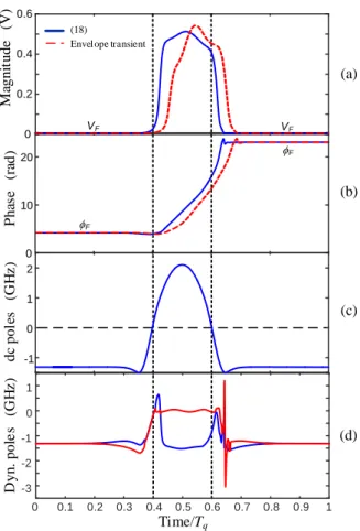
The results obtained when integrating system (18) are shown in Fig. 6(a) and Fig. 6(b), where a single time interval
n
I has been analysed. The nonlinear behaviour of the SRO is easily gathered from the shape of the pulse amplitude. When the pulse is on, the slope of the phase variable agrees with the beat frequency fofp, since the autonomous oscillation
contains the two frequency components. This beat frequency gives rise to small undulations at the top of the pulse, which will be more noticeable in the next example. The results from (18) are compared with those obtained through circuit-level envelope-transient simulations. There are some small discrepancies, attributed to a high sensitivity of the oscillator about the quench-signal parameters Vdc = ‒1.3 V, Vp = 0.9 V. As will be shown, discrepancies are smaller in our next experiment, for different quench-signal values.
The pulse in Fig. 6(a) can be related to the stability properties of the dc solution (obtained when suppressing the input source and replacing
( )t with a variable dc voltage), and with the dynamic poles, calculated through the periodic pulse. Using (18), the stability of the dc solution can be determined replacing the quench signal with a time-constant parameterGS V
and leading the system to linear regime, by reducing the amplitude of the input source Gin. Setting the fundamental frequency of system (15) to the frequency of the small-signal source, the forced solution will be time constant in the envelope-domain system (18) and given by xF, where the subscript F indicates forced operation. According to the averaging theorem [28], the stability properties of the small-signal solution xF agree with those of the dc solution (with Ig = 0). The stability of xF is determined by the eigenvalues ofthe constant Jacobian matrix f x V( F, GS) x, denoted as “dc poles”. According to this analysis, the dc solution is stable for
0.577 GS
V V. Beyond VGS 0.577V, the solution is unstable with a pair of complex-conjugate poles at about the oscillation frequency p.
Fig. 6(c) presents the variation of the dc poles through the excursion of the quench signal. As seen in Fig. 6(a) and Fig. 6(b), for stable dc poles, the solution amplitude exhibits
negligible value VF and the phase
( )t exhibits a constant shift F
with respect to the RF source phase . When the poles p 0 are on the right hand-side of the complex plane (RHS), there is a growth of the oscillation pulse until the saturation amplitude is reached. In fact, the dc poles cannot provide any information on the dynamics of the oscillation pulse when the pulse amplitude is large enough to excite the system nonlinearities. However this amplitude decays quickly when the dc poles return to the left hand side (LHS), as shown in Fig. 6(a). One should emphasize the consistency between the results of the envelope-domain equation (18) and the stability analysis of a small signal solution based on the same equation.The above analysis of the dc poles can be complemented with a linearization of system (18) through the oscillatory solution. In the neighbourhood of each point xq x t( )q of the pulsed oscillation, the trajectory will be expressed as
(q ) q ( )
x t t x x t . Then, the dynamics of the small deviation x t( ) can be approached as:
( ) ( ), (0) 0 , ( ) , ( ) , q q q q q q q q q x t f Df x t x f x t f f x t Df x (20)And the solution of linear time-invariant (LTI) system (20) has the form: 1( ) 2( ) 1 2 ( ) ( )( tq t 1) ( )( tq t 1) q q x t C t e C t e (21)
where 1( )tq and 2( )tq are the eigenvalues of the matrix Dfq and C t1( )q ,C t2( )q are vector coefficients determined by
0( )
q q
x x t and xq x t0( )q . When reaching the saturated amplitude, one of the eigenvalues becomes negative and the other one approaches a zero value, in consistency with the invariance of a free-running oscillation versus time shifts.
To illustrate further the prediction capabilities of the new formulation, a different implementation of the quench signal
( )t VGS( )t
will also be considered, with a quench frequency fq = 4 MHz. This quench signal has a larger period Tq, giving rise to a more pronounced nonlinear effect, since the system spends a longer time in the unstable region. In Fig. 7(a) and Fig. 7(b) the amplitude and phase obtained with (18) are compared with the ones resulting from circuit-level envelope-transient simulations. As stated, the local maxima and minima at the top of the waveform are due to the beat frequency, since the system remains long enough in saturated regime for this frequency to be observed. Fig. 7(c) shows the experimental measurements of the SRO signal, carried out with a Keysight Infiniium DSO90804A digital storage oscilloscope. The top of the pulse exhibits the same local maxima and minima observed in simulation.Fig. 6. Nonlinear semi-analytical formulation applied to a FET-based SRO, considering the input-signal power Pin = ‒53 dBm and frequency
fp = fo ‒ 90 MHz. The quench signal is (t) = VGS(t) = Vdc + Vpcos(ωqt), with
Vdc = ‒1.3 V, Vp = 0.9 V and fq = 7 MHz. (a) Magnitude of the SRO obtained with (18). The circuit-level envelope-transient simulation is superimposed. (b) Phase of the SRO obtained with (18). (c) Real part of dc poles of solutionxF versus time when considering static conditions. (d) Real part of dynamical poles calculated through the linearization of (18) about the oscillatory solution in (a) and (b).
Fig. 7. Prediction capabilities of (18), considering the input-signal power Pin = ‒ 53 dBm and frequency fp = fo ‒ 90 MHz.. The quench signal is (t) = VGS(t) = Vdc + Vpcos(ωqt), with Vdc = ‒1.3 V, Vp = 0.9 V and fq = 4 MHz, giving rise to a more pronounced nonlinear effect. (a) Magnitude of the SRO. Because the system trajectory remains more time in the unstable region, the beat frequency can be observed, producing multiple minima and maxima with small excursions at the top of the pulse. (b) Phase of the SRO. Magnitude and phase of the circuit-level envelope-transient simulations are superimposed in (a) and (b). (c) Experimental measurements of the SRO signal, carried out with a Keysight Infiniium DSO90804A digital storage oscilloscope.
IV. COMPACT NOISE ANALYSIS IN LINEAR AND NONLINEAR MODES
The main purpose of the semi-analytical model of Section III is to enable a stochastic characterization of the SRO in both linear and nonlinear mode. Here, the noise analysis is carried out.
A. Noise Analysis in Linear Mode
The envelope model (2) can be derived particularizing the semi-analytical formulation (15) to the linear-operation mode. The LTV transfer function H t( , p) will be calculated by replacing the RF source in (15) by an equivalent noise current source n t( )N t e( ) j(p)t
, at the analysis node. This equivalent source must account for all the circuit noise sources. Following the procedure explained in Section II.A to calculate the LTV transfer function, the noise source is replaced with an auxiliary deterministic small-signal source j( p )t
Ge . The resulting equation is the following:
1 ( ), p / 1( )
I Y t s j X t G (22) where G is the small magnitude of the equivalent noise source and X t1( ) is the first harmonic perturbation response to
this source. This component is related to the input source through the LTV transfer function:
1( ) ( , p)
X t H t
G (23) Note that, in the linear case, the amplitude variable is very small, so the dependence of the admittance function on V t( )has been neglected in (22). Applying the time derivative operator s, equation (22) provides:
( ), ( , ) ( ), ( , ) 1 p p p p Y t H t jY t H t (24)
In Fig. 8, the LTV transfer function H t f( , ) calculated from the semi-analytical formulation (24) is compared with the obtained with the circuit-level envelope transient method that was applied in Section II.D to the FET-based SRO of Fig. 2. Now, using the LTV transfer function calculated from (24), one can directly apply the whole stochastic characterization of the SRO in linear mode derived in Section II.
The S/N predicted with the semi-analytical formulation (24) , for the same operation conditions considered in Section II, is shown in Table I, where it can be compared with the one obtained with the LTV transfer functions.
0 10 20 0 0.2 0.4 0.6 0 1 2 -1 Time/Tq dc po le s (G H z ) M agni tude (V ) (a) (c) P ha se (ra d ) (b) (18)
Envel ope transient
0 0.1 0.2 0.3 0.4 0.5 0.6 0.7 0.8 0.9 1 -3 -2 -1 0 1 D yn . pol e s ( G H z ) (d) VF VF F F (a) (b) Time/Tq 0 0.4 0.8 1.2 1.6 2 0 0.1 0.2 0.3 P ha se (ra d) 10 30
50 (18)Envel ope transient
A m pl it ud e (V ) 0.2 0.4 0.6 (18)
Envel ope transient
0 M ea sure d A m pl it ude (V ) (c)
Fig. 8. Semi-analytical model. Magnitude of the harmonics H k( ) defined in (6) for k=0,3,5 of the LTV transfer function H t f versus the ( , ) frequency f. A quench signal of fq = 8 MHz has been applied. Comparison of the results of equation (24) (semi-analytical) with those of the circuit-level envelope transient simulation.
B. Noise Formulation in Nonlinear Mode
Let the solution of the SRO in nonlinear mode be denoted
0 ( ) ( )
x t x t . In the presence of noise sources, the system solution undergoes a perturbation of the form
0
( ) ( ) ( )
x t x t x t . Taking into account the small amplitude of the noise sources, the system governing the perturbation component x t( ) can be obtained through a linearization of system (18) about the unperturbed solution x t0( ), which
provides: 0 0 ( ) ( ) ( ), ( , ( )) ( , ( )) ( ) , ( ) x A t x B t n t f x t f x t A t B t x n (25)
where n t( ) is the vector containing the time-varying phasors of the noise sources. The solution of linear time-variant (LTV) system (25) is given by:
0
( ) ( , 0) (0) ( , ) ( ) ( )
t
x t t x t s B s n s ds
(26)where ( , )t s is the fundamental-solution matrix of system (25), fulfilling ( , )t s A t( ) ( , )t s and ( , )s s I, where I is the identity matrix. For ts, each column of this matrix provides the response of each state variable of system (25) to an impulse in ts. Since T is much bigger than the q
oscillation period 1/p, for each time value t, the components of ( , )t s become negligible for s . Due to the initial t Tq
condition, the oscillation envelope undergoes a transient of one cycle. After this transient, system (26) can be approached by:
( ) ( , ) ( ) ( ) q t t T x t t s B s n s ds
(27)Then, the correlation matrix of the vector process x t( )is given by: 1 1 1 1 2 2 1 2 ( ) ( ) ( ) ( , ) ( ) ( ) ( ) ( ) ( , ) ( , ) ( ) ( ) ( , ) q q q t t t t t t t T t T t t t t T C t x t x t t s B s n s n s B s t s ds ds t s B s B s t s ds
(28) where ( ) ( )1 2 (1 2) tn s n s s s . The diagonal components
of matrix C t( ) are the amplitude and phase variances V2( )t and 2
( )t
. Due to the periodic behavior of the SRO, the phase process is cyclostationary, with the periodic variance ( )t
2 ( )t
. Taking into account the theory of cyclostationary processes described in Section II.B, one can also calculate the noise power associated with the phase process. The correlation of the phase process is expressed in a Fourier series, with the quench frequency as fundamental:
( , ) ( ) ( ) ( ) jk qt
k k
R t t t
R e (29) And the variance fulfils 2( )t R t( , 0)
. The term k 0 of the series (29) enables the calculation of the power spectral density (PSD) of the phase process as [22]-[23]:
0 ( ) ( ) j S R e d
(30)From equation (30), the component R0( )
can be related to the
phase PSD using the inverse Fourier transform as:
0( ) ( ) j R S e d
(31)Finally, the noise power associated with the phase process is:
2 0 0 0 1 1 ( ) (0) ( , 0) ( ) q q T T q q P S d R R t dt t dt T T
(32)Equation (32) shows that the phase noise power in the whole quench interval is given by the mean value of the periodic variance 2( )t
. However, in practice, the only relevant noise power is the one generated during the interval [Ta, Tb] of the quench signal period in which the circuit oscillates:
2 2 , 1 ( ) ( ) b a T osc osc q T P t t dt T
(33)In most cases, the noise power resulting from the phase variance will dominate the one resulting from the amplitude variance. This will be shown in the following examples.
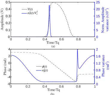
The analysis in B will be illustrated through its application to the Van der Pol-type SRO of Fig. 9, with element values shown in the caption. For R 33.3 , this circuit exhibits an oscillation at the frequency fo ≈ 1.6 GHz. The quenching action is implemented with a time-varying resistance R(t) = R0 + R1cos(ωqt). The quench frequency has been set to fq = 1 MHz, and an input current source has been considered, at the frequency fp = fo + 7 MHz. The PSD of the input white noise source is = 10-22 A2/Hz.
In Fig. 10(a) the normalized amplitude variance V2( ) /t Vo2,
where Vo = 0.5 V is the saturated oscillation amplitude, has been represented in the time interval [0, Tq]. This variance can be compared with the amplitude of the SRO pulse in the absence of noise sources. As gathered from the figure, the amplitude noise will have a stronger impact during the fast amplitude transient of V t( ) towards the autonomous oscillation. In Fig. 10(b), the phase variance 2( )t
have been represented in the time interval [0, Tq], where it can be compared with the instantaneous variation of the pulse phase, in the absence of noise sources. As can be seen, in this case, the phase variance is larger than the normalized amplitude variance. Note that, in nonlinear mode, the circuit self-oscillation is due to the sensitivity of each pulse to the remnant of the previous pulses, which are not fully extinguished [1], [6]. Thus, the amplitude and phase perturbations keep evolving in the quenched intervals, which will have an effect on the noise behavior in the “on” intervals. In fact, the amplitude and phase variables are continuous functions of time.
As shown in Fig. 10(a), the amplitude is more sensitive to the noise sources during the fast growing transient. On the other hand, the phase variance 2( )t
[Fig. 10(b)] is much larger when the oscillation is off, which is due to the small amplitude of the forced solution xF. The forced amplitude VF is very small and its phase is very sensitive to the noise perturbation. In the particular case of Gin=0 (absence of RF signal), this amplitude is VF=0, making the phase perturbation grow unboundedly.
However, when the oscillation is turned on, the variance
2( )t
decreases to a nearly constant value. The variation of
2( )t
is monotonous when the oscillation starts and exhibits a resonant peak when it is extinguished. This behaviour is consistent with the phase variation shown in the same figure, since the peak coincides with the fast phase transient of
( )t towards the forced solutionxF. In a manner similar to the amplitude behaviour shown in Fig. 10(a), the SRO phase is very sensitive to the noise sources during its fast transients.Fig. 9. Parallel-resonant Van der Pol-type oscillator, with L = 1 nH, C = 10 pF. The negative resistance is provided by a cubic nonlinear current source
3
( )
I v Av Bv , where A = ‒0.03 A/V and B = 0.01 A/V3. The quench signal
has been modelled by a time-varying resistance R t( )R0R1cosqt, where
0 31
R , R 1 4 , giving rise to the oscillation at R 34 . The quench frequency has been set to fq = 1 MHz, and the amplitude of the RF current source is Ig = 0.1A.
Fig. 10. Noise analysis of the Van der Pol-type SRO considering the particular input-signal power Pin = ‒ 93 dBm, when fp = fo + 7 MHz for the quench frequency fq = 1 MHz. (a) Normalized amplitude variance V2( )t in the time
interval [0, Tq], where Vo = 0.5 V. (b) Phase variance
2 ( )t
in the time interval [0, Tq]. The magnitude and phase in the absence of noise sources have also been represented in (a) and (b) respectively. The phase noise power generated during
the oscillation interval is 2 2
,osc ( )osc 0.1195 rad
P t .
It is interesting to note that the resonant peak in 2( )t
takes place when there is a significant difference between the phase at the end of the oscillation and the phase of the forced solution
F
. Whereas in the amplitude variance V2( ) /t Vo2 this resonantpeak will always exists because of the exponential growth at the beginning of the pulse, the peak in the phase variance 2
( )t
will not always be observed. This is illustrated in Fig. 10, showing the amplitude and phase variance when fp = fo + 10 MHz. Under this new condition, the phase difference at the end of the pulse is reduced and the resonant peak in 2( )t
no longer exists [Fig. 11(b)].
As already stated, the reduction of the phase variance 2 ( )t
is due to the increase in the signal amplitude when the oscillation is on. A non-oscillatory circuit with comparable signal amplitude would exhibit a much lower phase variance. To illustrate this, a constant resistor R = 31.5 has been considered in the circuit of Fig. 9, for which there is no oscillation. The input-source amplitude has been set to Ig = 1 mA, which provides a node-voltage amplitude of 0.35 V, in the order of that of the SRO. In these conditions, the phase variance is constant and given by 2 8.3 10 rad9 2
, many orders of magnitude below that of the SRO.
On the other hand, as gathered from Fig. 10 and Fig. 11, under a sufficiently high quench frequency, flicker noise
R(t) L C v I(v) ig(t) n(t) 0 0.2 0.4 0.6 0.8 1 0 0.1 0.2 0.3 0.4 0.5 0 5 10 15 20 25 Time/Tq A m pl it ude ( V ) N orm . A m pl it ude va ri anc e ( x 10 -3) V(t) σV2(t)/Vo 2 0 0.2 0.4 0.6 0.8 1 -6 -4 -2 0 2 4 0 0.4 0.8 1.2 1.6 2 Time/Tq P ha se ( ra d ) P ha se v ari anc e (ra d 2 ) (t) σ2(t) (a) (b)
sources will not have any impact on the SRO behavior. Note that phase-noise perturbations do not accumulate when the oscillation is quenched. This is because, in the quenched time intervals, the circuit behaves as a forced one, following the independent input source. During these intervals, the phase variable is restored to the value forced by the RF generator, and, therefore, the phase perturbation does not accumulate. This effect can be observed in Figs. 6(b), 7(b), 10(b) and 11(b), where the phase variable takes the same value (in 2π-module) in the initial and final quenched time intervals. The accumulation of the phase perturbation can only have an effect during oscillation pulses. However, due to the low frequency spectrum of the flicker noise source, under most practical values of the quench frequency fq, it will not have a significant impact during the short oscillation pulses.
Fig. 11. Noise analysis of the Van der Pol-type SRO considering the particular input-signal power Pin = ‒ 93 dBm, when fp = fo + 10 MHz for the quench frequency fq = 1 MHz. (a) Normalized amplitude variance V2( ) /t Vo2 in the
time interval [0, Tq]. (b) Phase variance
2 ( )t
in the time interval [0, Tq]. The phase gap at the end of the pulse is negligible, thus the resonant peak has been removed. The phase noise power generated during the oscillation interval is
2 2
,osc ( )osc 0.3174 rad
P t .
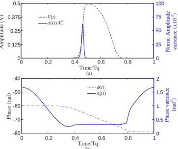
D. FET-based SRO in Nonlinear Mode
The noise analysis in Subsection B will also be applied to the FET-based SRO of Fig. 2, using the realistic admittance model extracted from HB simulations. An equivalent white noise source, accounting for the circuit noise contributions, is considered at the analysis port, having the spectral density = 10-22 A2/Hz. Fig. 12 shows the amplitude and phase
variances, V2( ) /t Vo2 and 2( )t
respectively, behaving as predicted in Subsection C, i.e., 2
( )t
decreases in the time interval where the system is oscillating. The phase noise power generated during the oscillation interval is
2 2
,osc ( ) osc 0.0033 rad
P t . This result has been
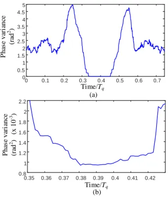
experimentally validated. To determine the phase variance of the experimental prototype, the output of the SRO was obtained with a Keysight Infiniium DSO90804A digital storage
oscilloscope. For this purpose, the period Tk of each RF cycle
was extracted from the measured output of the SRO. Then, this period was used to generate the random variable TpTk, where
p
T is the period of the input RF signal. Finally, taking into account that Tp Tq, the phase variance is approached by:
2 2 1 ( ) , 2 1 1 , 2 1 n k k i k i n n k i p p k i k k i i n t n T T n
(34)where tk is the time value at which the period Tk is measured,
and 2n + 1 is the number of samples about each tk considered
in the averaging. Fig. 13 shows the measured phase variance, and the phase noise power generated during the oscillation
interval is 2 2
,osc ( ) osc 0.0013 rad
P t , with good
qualitative agreement with the solution obtained from the noise formulation in Subsection A.
Fig. 12. Noise analysis of the FET-based SRO considering the particular input-signal power Pin = ‒ 60 dBm and frequency fp = fo ‒ 90 MHz. The quench signal is (t) = VGS(t) = Vdc + Vpcos(ωqt), with Vdc = ‒1.3 V, Vp = 0.9 V and fq = 4 MHz. (a) Normalized amplitude variance 2 2
( ) /
V t Vo
in the time interval [0, Tq]. (b) Phase variance
2 ( )t
in the time interval [0, Tq]. Note that
2 ( )t
decreases in the time interval where the system is oscillating, as predicted by the noise formulation in Subsection B. The phase noise power generated during
the oscillation interval is 2 2
,osc ( )osc 0.0033 rad
P t . Time/Tq 0 0.2 0.4 0.6 0.8 1 0 0.125 0.25 0.375 0.5 0 100 25 50 75 A m pl it ude ( V ) N orm . A m pl it ude va ri anc e ( x 10 -3) V(t) σV2(t)/Vo (a) 0 0.2 0.4 0.6 0.8 1 -80 -70 -60 -50 -40 0 1 2 Time/Tq P ha se ( ra d ) 0.5 1.5 P ha se va ri anc e (ra d 2 ) (t) σ2(t) (b) 2 0 0.1 0.2 0.3 0.4 0.5 0.6 0.7 0 0.05 0.1 0.15 0.2 0.25 0.3 0.35 A m pl it ude (V ) (a) N orm . A m pl it ude va ri anc e ( x 10 -3 ) 0 0.1 0.2 0.3 0.4 0.5 0.6 0.7 0.8 0.9 1 Time/Tq 0 0.1 0.2 0.3 0.4 0.5 0.6 0.7 0.8 0.9 1 0 10 20 30 0 10 20 30 P ha se ( ra d ) P ha se v ari anc e ( ra d 2 ) (x 10 -3 ) Time/Tq (b) 40 40 V(t) σV2(t)/Vo2 (t) σ2(t)
Fig. 13. Noise analysis of the FET-based SRO. Experimental results corresponding to the case simulated in Fig. 11. (a) Measured phase variance of the SRO in Fig. 2. (b) Zoomed view showing good qualitative agreement with the solution obtained from the noise formulation in Subsection B. The phase noise power generated during the oscillation interval is
2 2
,osc ( )osc 0.0013 rad
P t .
V. CONCLUSION
Methodologies for the noise analysis of SROs in linear and nonlinear modes, applicable to oscillators of arbitrary topology, have been presented. The analysis in linear mode is based on the calculation of one or more linear time-variant (LTV) transfer functions with respect to the noise source. These transfer functions are extracted from envelope-transient simulations at circuit level of the SRO, under small-signal sinusoidal excitations. Then, a stochastic analysis is carried out, taking into account the cyclostationary nature of the autocorrelation function of the output signal. This enables a straightforward determination of the output noise power spectral density and the signal-to-noise ratio. A second methodology is intended for a compact analysis of the SRO in both linear and nonlinear mode. It is based on a new reduced-order semi-analytical formulation of the SRO in the envelope domain. This relies on numerical nonlinear model of the oscillator circuit, extracted from harmonic-balance simulations, by replacing time-varying quench signal with a variable dc voltage. The formulation has been tested under a demanding nonlinear operation of the SRO, with irregular pulse shapes. A linearization of this formulation in the presence of noise sources enables the calculation of the variances of the oscillation amplitude and phase. The complex variation of the phase variance through the quench period has been investigated in detail and related to the time variation of the oscillation phase. The results have been
successfully compared with the variance obtained from experimental measurements.
REFERENCES
[1] F. X. Moncunill-Geniz, P. Pala-Schonwalder and O. Mas-Casals, "A generic approach to the theory of superregenerative reception," in IEEE Trans. Circuits Syst. I, Reg. Papers, vol. 52, no. 1, pp. 54-70, Jan. 2005. [2] H. Ghaleb, P. V. Testa, S. Schumann, C. Carta and F. Ellinger, "A
160-GHz Switched Injection-Locked Oscillator for Phase and Amplitude Regenerative Sampling," in IEEE Microw. Compon. Lett, vol. 27, no. 9, pp. 821-823, Sept. 2017.
[3] M. Vossiek and P. Gulden, "The Switched Injection-Locked Oscillator: A Novel Versatile Concept for Wireless Transponder and Localization Systems," IEEE Trans. Microw. Theory Techn., vol. 56, no. 4, pp. 859-866, Apr., 2008.
[4] M. Vossiek, T. Schafer and D. Becker, "Regenerative backscatter transponder using the switched injection-locked oscillator concept," 2008 IEEE MTT-S Int. Microwave Symp. Dig., Atlanta, GA, 2008, pp. 571-574. [5] J. Bonet-Dalmau, F. X. Moncunill-Geniz, P. Pala-Schonwalder, F. del Aguila-Lopez and R. Giralt-Mas, "Frequency Domain Analysis of Superregenerative Receivers in the Linear and the Logarithmic Modes," in IEEE Trans. Circuits Syst. I, Reg. Papers, vol. 59, no. 5, pp. 1074-1084, May 2012.
[6] S. Hernández and A. Suárez, "Analysis of Superregenerative Oscillators in Nonlinear Mode," IEEE Trans. Microw. Theory Techn., vol. 67, no. 6, pp. 2247-2258, June 2019.
[7] P. Palà-Schönwälder, J. Bonet-Dalmau, F. X. Moncunill-Geniz, F. del Águila-López and R. Giralt-Mas, "A Superregenerative QPSK Receiver," IEEE Trans. Circuits Syst. I, Reg. Papers, vol. 61, no. 1, pp. 258-265, Jan. 2014.
[8] P. Palà-Schönwälder, J. Bonet-Dalmau, A. López-Riera, F. X. Moncunill-Geniz, F. del Águila-López and R. Giralt-Mas, "Superregenerative Reception of Narrowband FSK Modulations," IEEE Trans. Circuits Syst. I: Reg. Papers, vol. 62, no. 3, pp. 791-798, March 2015.
[9] J. Ayers, K. Mayaram and T. S. Fiez, "A Low Power BFSK Super-Regenerative Transceiver," 2007 IEEE Int. Symp. Circuits Syst., New Orleans, LA, 2007, pp. 3099-3102.
[10] P. Pala-Schonwalder, F. X. Moncunill-Geniz, J. Bonet-Dalmau, F. del-Aguila-Lopez and R. Giralt-Mas, "A BPSK superregenerative receiver. Preliminary results," 2009 IEEE Int. Symp. Circuits Syst., Taipei, 2009, pp. 1537-1540.
[11] A. López-Riera, P. Palà-Schönwälder, J. Bonet-Dalmau, F. X. Moncunill-Geniz, F. del Águila-López and R. Giralt-Mas, "A proof-of-concept superregenerative QPSK transceiver," 2014 21st IEEE Int. Conf. on Electronics, Circuits and Systems (ICECS), Marseille, 2014, pp. 167-170.
[12] F. X. Kaertner, "Analysis of white and f-α noise in oscillators," Int. Journal of Circuit Theory and Applications, vol. 18, pp. 485-519, 1990 [13] A. Demir, "Phase noise and Timig Jitter in oscillators with colored noise
sources," IEEE Trans. Circuits Syst. I. Fundam. Theory Appl., vol. 49, pp. 1782-1791, December. 2002
[14] P. E. Thoppay, C. Dehollain and M. J. Declercq, "Noise analysis in super-regenerative receiver systems," 2008 Ph.D. Research in Microelectronics and Electronics, Istanbul, 2008, pp. 189-192. [15] D. Lee and P. P. Mercier, "Noise Analysis of Phase-Demodulating
Receivers Employing Super-Regenerative Amplification," IEEE Trans. on Microw. Theory Techn., vol. 65, no. 9, pp. 3299-3311, Sept. 2017. [16] S. Hernández, S. Sancho, A. Suárez, “Cyclostationary Noise Analysis of
Superregenerative Oscillators”, 2019 IEEE MTT-S Int. Microwave Symp. Dig., Boston, MA, 2019.
[17] L. A. Zadeh, "Frequency Analysis of Variable Networks," in Proceedings of the IRE, vol. 38, no. 3, pp. 291-299, March 1950. [18] S. Hernández and A. Suárez, "Envelope-Domain Analysis and Modeling
of Super-Regenerative Oscillators," in IEEE Trans. Microw. Theory Techn., vol. 66, no. 8, pp. 3877-3893, Aug. 2018.
[19] E. Ngoya and R. Larcheveque, "Envelop transient analysis: a new method for the transient and steady state analysis of microwave communication circuits and systems," IEEE MTT-S Int. Microwave Symp. Dig., San Francisco, CA, USA, 1996, vol.3, pp. 1365-1368. [20] K. S. Kundert, "Introduction to RF simulation and its application," in
IEEE J. Solid-State Circuits, vol. 34, no. 9, pp. 1298-1319, Sep 1999.
0 0.1 0.2 0.3 0.4 0.5 0.6 0.7 0 0.5 1 1.5 2 2.5 3 3.5 4 4.5 5 Time/Tq P ha se va ri anc e (ra d 2 ) (a) 0.35 0.36 0.37 0.38 0.39 0.4 0.41 0.42 0.8 1 1.2 1.4 1.6 1.8 2 2.2 P ha se va ri anc e (ra d 2 ) ( x 10 -3 ) Time/Tq (b)
[21] E. Ngoya and A. Soury, “Envelope Domain Methods for Behavioral Modeling”, Fundamentals of Nonlinear Behavioral Modeling for RF and Microwave Design. Artech House, 2005.
[22] J. Roychowdhury, D. Long and P. Feldmann, “Cyclostationary Noise Analysis of Large RF Circuits with Multitone Excitations”, IEEE J. Solid-State Circuits, vol. 33, no. 3, March 1998
[23] T. Ström and S. Signell, “Analysis of periodically switched linear circuits,” IEEE Trans. Circuits Syst., vol. CAS-24, pp. 531–541, Oct. 1977.
[24] A. Suárez, Analysis and Design of Autonomous Microwave Circuits. IEEE-Wiley, Hoboken, (NJ) Jan. 2009.
[25] F. Ramirez, M. Ponton, S. Sancho, and A. Suarez, "Phase-noise analysis´ of injection-locked oscillators and analog frequency dividers," IEEE Trans. Microw. Theory Tech., vol. 56, no. 2, Feb. 2008.
[26] S. Sancho, A. Suarez and F. Ramirez, "General Phase-Noise Analysis From the Variance of the Phase Deviation," IEEE Trans. Microw. Theory Tech., vol. 61, pp. 472-481, 2013
[27] J. de Cos and A. Suárez, "Efficient Simulation of Solution Curves and Bifurcation Loci in Injection-Locked Oscillators," IEEE Trans. Microw. Theory Techn., vol. 63, no. 1, pp. 181-197, Jan. 2015.
[28] S. Wiggins, Introduction to Applied Nonlinear Dynamical Systems and Chaos, Springer-Verlag, New York, 1990.
Sergio Sancho (A’04–M’04) received the degree in Physics
from Basque Country University in 1997. In 1998 he joined the Communications Engineering Department of the University of Cantabria, Spain, where he received the Ph.D. degree in Electronic Engineering in February 2002. At present, he works at the University of Cantabria, as an Associate Professor of its Communications Engineering Department. His research interests include the nonlinear analysis of microwave autonomous circuits and frequency synthesizers, including stochastic and phase-noise analysis.
Silvia Hernández (S’17) was born in the Canary
Islands, Spain. She received her M.S. degree in Telecommunication Engineering from the University of Las Palmas de Gran Canaria, Canary Islands, Spain, in 2015. The same year, she entered the Institute for the Technological Development and Innovation in Communications, University of Las Palmas de Gran Canaria, as a research assistant. In 2016, she joined the Communications Engineering Department, University of Cantabria, where she is currently working towards her Ph.D. degree.
Her research interests include stability analysis and the study of new methods for the analysis and design of nonlinear microwave circuits.
Almudena Suárez (M’96-SM’01-F’12) was born in
Santander, Spain. She received the degree in electronic physics and the Ph.D. degree from the University of Cantabria, Santander, Spain, in 1987 and 1992, respectively, and the Ph.D. degree in electronics from the University of Limoges, France, in 1993. At present, she is a Full Professor at the University of Cantabria, and a member of its Communications Engineering Department. She has authored the book Analysis and design of autonomous microwave circuits for the publisher IEEE–Wiley and co–authored the book Stability analysis of microwave circuits for the publisher Artech–House. She belongs to the technical committees of the IEEE International Microwave Symposium and European Microwave Conference. She was an IEEE Distinguished Microwave Lecturer for the period 2006–2008. She is an associate editor of the IEEE Microwave Magazine. She is a member of the Board of Directors of EuMA and the Editor in Chief of International Journal of Microwave and Wireless Technologies from Cambridge University Press.