Desing and Implementation of a CMOS Interface for Non Invasive Optical Biosensors Edición Única
76
0
0
Texto completo
(2) INSTITUTO TECNOLOGICO Y DE ESTUDIOS SUPERIORES DE MONTERREY MONTERREY CAMPUS GRADUATE PROGRAM IN MECHATRONICS AND INFORMATION TECHNOLOGIES The members of the thesis committee hereby approve the thesis of Eduardo Andres Barredo Ochoa as a partial fulfillment of the requirements for the degree of Master of Science with major in Electronic Engineering (Electronic Systems) Thesis Committee.
(3) DESIGN AND IMPLEMENTATION OF A CMOS INTERFACE FOR NON-INVASIVE OPTICAL BIOSENSORS BY EDUARDO ANDRÉS BARREDO OCHOA THESIS PRESENTED TO THE GRADUATE PROGRAM IN MECHATRONICS AND INFORMATION TECHNOLOGIES THIS THESIS IS A PARTIAL REQUIREMENT FOR THE DEGREE OF MASTER OF SCIENCE WITH MAJOR IN. ELECTRONIC ENGINEERING (ELECTRONIC SYSTEMS). INSTITUTO TECNOLÓGICO Y DE ESTUDIOS SUPERIORES DE MONTERREY MONTERREY CAMPUS. DECEMBER, 2009.
(4) To my parents who are always supporting me. To my sisters who have been giving all I need all these years. To all my friends who are in Ecuador making my holidays worth. To all does people that I have met in the last six year in Mexico making my instance great..
(5) Acknowledgements I w o u l d like to express my sincere gratitude to my advisor Professor Sergio O m a r M a r t i n e z for his a t t e n t i o n , k n o w l e d g e , and professional advises and friendship over these y e a r s . I a d m i r e his objectivity and patience to give the best advises. I a m truly thankful w i t h Professor G r a c i a n o Dieck for his friendship and his teaching experience in my professional career as my career director and as a f r i e n d , colleague and t e a c h e r in my master studies.. I w a n t to express my thanks to Professor A l f o n s o Avila for his. friendship all these years as a t e a c h e r and as my master director. I w a n t to say thanks to Luis Ernesto Saracho and A l f r e d o Farid for his f r i e n d s h i p , teaching and motivation at " L a b M E M S " , w i t h o u t their k n o w l e d g e this w o r k w o u l d n ' t be finish. I w a n t to give a special thanks t o Agustin Carvajal for his f r i e n d s h i p , help and support a r o u n d these years. Also, I w a n t to say thanks to all the p e o p l e at " L a b M E M S " and "La C u e v a " for their friendship and s u p p o r t . I w a n t t o give my most sincere thankful to all my friends that wasn't w i t h me at L a b M E M S but w e r e always supporting me out of the s c h o o l , especially A n d r e a Herrera and R o m m e l V a l e n c i a . Thanks to all my friends f r o m Ecuador w h o was always c o n c e r n e d about me. Finally, I want to express my gratitude to my family for their never-ending support. This work is a result of all your love and comprehension. Eduardo Andres Barredo Ochoa Instituto Tecnologico y de Estudios Superiores de Monterrey Dec, 2009. i.
(6) ii.
(7) DESIGN AND IMPLEMENTATION OF A CMOS INTERFACE FOR NON-INVASIVE OPTICAL BIOSENSORS Eduardo A n d r e s Barredo O c h o a , M.S. Instituto T e c n o l ó g i c o y de Estudios Superiores de M o n t e r r e y , 2009 Thesis Advisor: Sergio O m a r M a r t i n e z Chapa, Ph.D.. Abstract In this thesis, I propose an o p t o e l e c t r o n i c interface as those required in non-invasive micro sensors. The interface w a s i m p l e m e n t e d on a 0.35u.m C M O S t e c h n o l o g y a n d consists of a p h o t o d i o d e t o capture a n d t r a n s f o r m light into a current, a n d an amplifier to convert this current into a voltage level. I have designed t h r e e different p h o t o d i o d e s . Because of their structures, they are called p+/nwell,. n+/p-substrate,. nwell/p-substrate. photodiodes.. Additionally,. I. have. i m p l e m e n t e d t h e spatially m o d u l a t e d t e c h n i q u e in o r d e r t o increase the p h o t o d i o d e s b a n d w i d t h . The required ring t o avoid interference a n d t o protect the input pads had also been i n c o r p o r a t e d in the layout. I have r e v i e w e d m a t h e m a t i c a l a p p r o x i m a t i o n s that describe t h e p h o t o c u r r e n t in t h e f r e q u e n c y d o m a i n . These a p p r o x i m a t i o n s c o u l d be used in later studies a i m e d t o characterize p h o t o d i o d e . Finally, the amplifier consists on a current t o voltage c o n v e r s i o n , a b a n d w i d t h expansion m o d u l e a n d a voltage amplifier. The amplifier has s h o w e d a t r a n s i m p e d a n c e of 47 ^/ j[, a frequency b a n d w i d t h of 8 5 2 M H z a n d a g a i n - b a n d w i d t h of 2GHz. m. iii.
(8) iv.
(9) Contents Acknowlegments. i. Abstract. iii. 1. Introduction. 1. 1.1.. Problem Statement. 2. 1.2.. Objectives. 3. 1.3.. Thesis outline. 3. 2. State of the art 3. Photodiode with a CMOS technology. 4 11. 3.1.. Introduction. 12. 3.2.. Ideal photodiode. 13. 3.3.. Absorption light in silicon. 13. 3.3.1. 3.4.. Photodiode design. 3.4.1. 3.5.. An easy approach of the photocurrent. 15 16. Photodiodes main variants. 17. Bandwidth of photodiodes in CMOS. 19. 3.5.1.. Nwell/p-substrate, high resistance and twin well technology. 19. 3.5.2.. Nwell/p-substrate photodiode with low-resistance substrate and twin technology. 26. 3.5.3.. Nwell/p-substrate photodiode with high-resistance substrate and separated wells. 28. 3.5.4.. N+/p-substrate with high-resistance substrate and separated wells. 29. 3.5.5.. P+/Nwell/p-substrate with low-resistance substrate and adjoined wells. 29. 3.6.. Scope and limitations of CMOS photodiodes. 30. 3.6.1.. Wavelength limitations. 31. 3.6.2.. Bandwidth and responsivity comparison. 31. 3.6.3.. Parasites comparison. 33. 4. Simulation and design of an optoelectronic interface 4.1.. P+/nwell photodiode design in a 0.35^m CMOS technology. 4.1.1. 4.1.2.. Designed blocks Node designs of the p+/nwell photodiode. 34 35 36 36.
(10) 4.1.3. 4.2.. Guard bands design. Nwell/p-substrate photodiode design. 4.2.1.. Node designs of the nwell/p-substrate photodiode. 38 39 40. 4.3.. N+/p-substrate photodiode design. 42. 4.4.. Spatially modulated photodiode designs. 43. 4.5.. Ring design. 44. 4.6.. High bandwidth amplifier design. 46. 4.6.1.. Transimpedance amplifier. 47. 4.6.2.. Current source. 50. 4.6.3.. Analog equalizer. 51. 4.6.4.. Voltage amplifier. 56. 4.6.5.. Simulation results. 56. 5. Conclusions and futures work. 60. 5.1.. Conclusions. 60. 5.2.. Future works. 61. Bibliography. 62.
(11) List of Figures Figure 1.1: Electric diagram of an optical sensor. Figure 1.2: Control system of the glucose level. Figure 2.1: Diagram of the miniature CMOS optical biosensing system. Figure 2.2: P+/nwell Yu-Wei's photodiode. Figure 2.3: Yu-Wei's circuit amplifier. Figure 2.4: Spatially modulated light detector Figure 2.5: Bode diagram of the SML-detector electron current response compared to the conventional CMOS detector (dashed line). Figure 2.6: Structure of Complementary APS architecture. Figure 2.7: Layout of a complementary APS with a 0.25u.m CMOS technology. Figure 2.8: SPS general structure. Figure 2.9: Possible SPS implementation. Figure 2.10: Photodiode backup circuit. Figure 2.11: Differential photodiode pair. Figure 2.12: Amplifier for a differential photodiode. Figure 2.13: Proposed hybrid structure of CMOS/PD/VCSEL. Figure 3.1: Electromagnetic spectrum. Figure 3.2: Characteristic curve of the photodiode. Figure 3.3: Absorption coefficient 3 versus wavelength. Figure 3.4: Responsivity of Si, Ge and InGaP photodiode. Figure 3.5: Cross view of 0.35u.m CMOS technology layers. Figure 3.6: Finger nwell/p-substrate photodiode structure with high resistance substrate and twin-wells in standard CMOS technology. Figure 3.7: Finger nwell/p photodiode structure with low-resistance substrate and twinwells in standard CMOS technology. Figure 3.8: A finger nwell/p-substrate photodiode structure with high resistance substrate and separate-wells standard CMOS technology. Figure 3.9: Finger n+/p-substrate photodiode with high-resistance substrate Figure 3.10: Finger p+/nwell/p-substrate photodiode structure with low-resistance substrate and adjoined-wells. Figure 3.11: The boundary conditions for hole densities inside nwell. Figure 3.12: Amplitude of the double Fourier series of the nwell diffusion current for the vertical and the lateral nwell direction. Figure 3.13: Phase of the double Fourier series of the nwell diffusion current for the vertical and the lateral nwell direction Figure 3.14: The total amplitude and phase of the nwell diffusion current. Figure 3.15: Frequency response of the substrate diffusion current Figure 3.16: The calculated total photocurrent response of nwell/p-substrate photodiode with high-resistance substrate in a twin-well technology: 2 u.m (solid lines) and 10 u.m nwell size (dashed lines) for X = 850 nm. Figure 3.17: The calculated amplitude response of nwell/p-substrate photodiode with. 1 2 5 5 5 6 6 7 7 8 8 8 9 9 10 12 13 14 16 16 17 18 18 18 19 20 21 22 22 24. 26 27.
(12) low-resistance substrate in a twin-well technology: 2 u.m (solid lines) and 10 u.m nwell size (dashed lines) for X = 850 nm. Figure 3.18: The measured DC photocurrent of nwell/p-substrate photodiode Figure 3.19: The measured (line) and calculated (dashed) responses of a nwell/psubstrate photodiode with 2 u.m nwell-size, X = 850 nm. Figure 3.20: The response of nwell/p-substrate photodiode with high-resistance substrate in a separate-wells technology: 2 um (solid lines) and 10 um nwell size (dashed lines) for X = 850 nm. Figure 3.21: The boundary conditions for the hole density inside the nwell for the double-photodiode. Figure 3.22: The response of p+/nwell/p-substrate photodiode with lowresistance substrate in an adjoined-wells technology: 2 um (solid lines) and 10 um nwell size (dashed lines) for X = 850 nm Figure 3.23: Photodiode equivalent circuit. Figure 4.1: P+/nwell photodiode. Figure 4.2: P+ fingers of p+/nwell photodiode. Figure 4.3: Pnode connection of p+/nwell photodiode. Figure 4.4: Nnode connection of p+/nwell photodiode. Figure 4.5: Guard bands of p+/nwell photodiode. Figure 4.6: Internal ring connection. Figure 4.7: Nwell/p-substrate photodiode. Figure 4.8: NTUB+DIFF layers of the Nnode connection. Figure 4.9: NTUB+DIFF+CONT layers of the Nnode connection. Figure 4.10: NTUB+DIFF+CONT+MET1 layers of the Nnode connection. Figure 4.11: NNODE connection of nwell/p-substrate. Figure 4.12: Pnode connection of nwell/p-substrate. Figure 4.13: N+/p-substrate photodiode. Figure 4.14: A Nwell/P-substrate spatially modulated photodiode in 0.35u.m CMOS technology. Figure 4.15: A N+/P-substrate spatially modulated photodiode in 0.35u.m CMOS technology. Figure 4.16: Ring design. Figure 4.17: Photodiodes with ring. Figure 4.18: Block diagram of a high bandwidth amplifier. Figure 4.20: Schematic representation and ideal model of the transimpedance amplifier. Figure 4.21: Common-Gate circuit as a transimpedance amplifier. Figure 4.22: Improved circuit for transimpedance amplifier. Figure 4.23: Common source as a transimpedance amplifier. Figure 4.24: TIA design. Figure 4.25: Threshold current reference. Figure 4.26: Analog equalizer. Figure 4.27: Inductive peaking schematic. Figure 4.28: Inductive peaking design. Figure 4.29: CMOS inverter design.. 28 28. 29 30. 30 33 35 37 37 38 39 39 40 40 41 41 42 42 43 43 44 45 46 46 47 48 48 48 49 50 51 52 52 54.
(13) Figure Figure Figure Figure Figure Figure Figure. 4.30: Source degeneration circuit. 4.31: Voltage amplifier. 4.32: DC analysis 4.33: AC analysis. 4.34: Transient analysis. 4.35: A closed view of the transient analysis. 5.1: Input current instrumental amplifier.. 55 56 57 58 59 59 61.
(14) Chapter 1 Introduction. A non-invasive sensor is the one which does not produce any perturbation in the measured system. In the case of biological systems, this perturbation is related to pain or infection. Light provides a useful technique to get information about physiological parameters. Biosensors using light are considered non-invasive. The optical interface of this kind of sensor consists of two blocks, a photodiode and an amplifier. An electric diagram of an optical sensor is shown in the Figure 1.1. In this figure, the triangular block represents the amplifier, and the resistance Rf the amplifier factor.. Figure 1.1: Electric diagram of an optical sensor.. 1.
(15) It is a challenge to make a long lasting non-invasive biosensor. Researchers believe that miniaturizing the biosensor can reduce costs and obtain higher device longevity. One step to miniaturize the optical biosensor is miniaturizing the phototransistor or photodiode. It can be done by using Complementary Metal and Oxide Semiconductors (CMOS) technology (1). It would be very useful because transistors can be made with the same process. This means that the same integrated circuit contains the photodiode and the amplifier. Near-Infrared Spectroscopy (NIRS) are used to analyze the signal frequency behavior when the incident light is close to the near infrared range. That means when the wavelength range is 800nm-2.5μm.. 1.1. Problem Statement The BioMEMS Research Group at Instituto Tecnologico y de Estudios Superiores Monterrey (ITESM), Monterrey Campus is developing an insulin supply system. Therefore, it will be very useful an optical biosensor to watch and control the glucose levels in diabetes patients. Control the glucose level and automate the supply of insulin would be very helpful for the patients who suffer diabetes because this way they can optimize the use of insulin and they could supply insulin whenever is needed. To close the closed-loop control system it is necessary a biosensor which sense the glucose level. The control system can be represented as shown in Figure 1.2.. Figure 1.2: Control system of the glucose level.. The biosensor has to be sensible to the concentration of molecules of glucose to give an electronic signal which represent this concentration.. 2.
(16) 1.2. Objectives The main objective of this thesis is to design a miniaturized optical sensor with CMOS technologies, and the electronic circuit needed to sense an optical signal. The sensor will be needed by the B i o M E M S Research Group to develop the glucose control in diabetes patients. The specific objectives of this thesis are: Research the photodiode behavior in order to find a way to simulate its operation. Understand its limitations due to a technology and process constraint. Research photodiode layout techniques. Design different photodiodes layouts. Incorporate the layouts of the pads in order to fabricate photodiodes. Research the main characteristics of the amplifier that will to sense the photocurrent. Look for different topologies of the amplifier to obtain high bandwidth. Capture and simulate the amplifier.. 1.3. Thesis outline This thesis is organized in five chapters. The distribution of these chapters is as follow. Chapter 1 presents an overview of the problem, introduction of the most important concepts; and the main and specifics objectives. Chapter 2 describes the state of the art of optoelectronic interfaces. This chapter shows the previous work related with the optical electronic interfaces. Chapter 3 describes the way to implement photodiodes with a CMOS technology. This chapter also reviews mathematical approximations that describe the photocurrent in the frequency domain. Chapter 4 shows the design of the optoelectronic interface captured and simulated. The first part shows three different kinds of photodiodes with all the layers needed. The second part shows the design of the amplifier with the equations, considerations and specifications. The chapter also includes simulations of the amplifier stage. Chapter 5 has the conclusions and future works related with this thesis.. 3.
(17) Chapter 2 State of the art This chapter presents some previous investigations related with this thesis. The applications optoelectronic interfaces in a sensor are many, but they can be divided in two approaches: Those interfaces that are related to spectrometry and those related to image capture. Concerning the first approach, the objective is to get the spectrum of a signal in the frequency domain. Concerning the second approach, the goal is to obtain different readings or scans of luminance and chrominance in space domain. Yu-Wei Chang et al (2) have designed a high-sensitivity CMOS-Compatible system. They designed a complete optoelectronic interface to sense physiological parameters like H2O2, histamine and glucose. A diagram of the CMOS optical biosensing system is shown in the Figure 2.1. Chang et al (2) has designed a p+/nwell photodiode with two rings used to keep it out of noise. The Figure 2.2 and Figure 2.3 show the photodiode layout and the amplifier schematic. A better explanation of the p+/nwell photodiode design is shown in the next chapter 4.. 4.
(18) 5.
(19) Jan Genoe et al (3) designed a spatially modulated light detector (SML-detector). It consists in a nwell/p-substrate photodiode with a extra layer of metal over the half of nwell's fingers. Figure 2.4 shows the SML-detector. The graphic on the right of the Figure 2.4 shows the normalized responsivity as a function of the bit-rate. A flat I-D curve is obtained up to 500 Mb/s.. Figure 2.4: Spatially modulated light detector. Figure 2.5 shows the bandwidth of the SML-detector. The bandwidth is much higher than the conventional CMOS photodiode.. Figure 2.5: Bode diagram of the SML-detector electron current response compared to the conventional CMOS detector (dashed line).. 6.
(20) Cheng Xu et al (4), shows the design of an Active Pixel Sensor (APS) using a CMOS technology of 0.25u.m. In order to capture an image, a matrix of APS is needed. The Figure 2.6 shows the schematic circuit of one pixel. Pixel cell Rs. Figure 2.6: Structure of Complementary APS architecture (4).. A layout of the APS designed by Cheng Xu et al is appears in Figure 2.7. The fill factor (the relation between the entire APS and the photodiode) is 30%.. Figure 2.7: Layout of a complementary APS with a 0.25^m CMOS technology.. 7.
(21) Alexander Fish et al (5), designed a selft-powered CMOS Active pixel sensor (SPS) architecture. The idea is to use a photodiode for self power generation. The element to provide the power to the system is called power generation photodiode (PGPd). A schematic diagram of a SPS general architecture is shown in Figure 2.8.. Figure 2.8: SPS general structure (5).. An implementation of a possible SPS is shown in Figure 2.9. In this photodiode application a backup circuit is necessary because the power photodiode depends on illumination levels. A. Fish (5) designed a backup circuit which appears in Figure 2.10.. Figure 2.9: Possible SPS implementation (5).. Figure 2.10: Photodiode backup circuit (5).. 8.
(22) Markus Grözing et al (6) designed a front-end amplifier for integrated differential photodiodes. The technology used by them was a 0.18µm CMOS technology. The differential photodiode consist of a pair n+/nwell/p-substrate photodiodes connected together having a metal shading mask over one of the two photodiodes. The Figure 2.11 shows a diagram with the pair of photodiodes.. Figure 2.11: Differential photodiode pair (6).. A schematic of the differential amplifier appears in Figure 2.12. The circuit consists of a lownoise transimpendace amplifier (TIA) connected to a high-gain limiting amplifier (LIA). The output driver reduces the output impedance. The TIA converts the current to voltage, the LIA amplifies the voltage signal and the driver provides low output impedance.. Figure 2.12: Amplifier for a differential photodiode (6).. As was explained before, spectroscopy is very useful to obtain information about different parameters. But unfortunately the silicon does not have a good performance for wavelength higher than 0.95µm. This limitation has found new interest in researchers to find other semiconductors such as GaAs (Gallium Arsenide) to provide better performances at higher wavelengths.. 9.
(23) Tatsushi Nakahara et al (7) proposed an hybrid photodiode which consists of using both, a silicon CMOS, and a GaAs wafers. To integrate both wafers, a polyimide layer is used as shown in Figure 2.13.. Figure 2.13: Proposed hybrid structure of CMOS/PD/VCSEL (7).. CMOS technologies are very popular for designing optoelectronic interfaces mainly because the cost of the integrated circuit. Moreover, CMOS technologies allow a monolithic solution incorporating photodiodes and circuits in the same chip. CMOS sensors became very popular for image capture. Nowadays, they are incorporated in video cams. Concerning spectrometry, the silicon is limited to wavelengths in the range from 400nm to 1um. Anyway, it is possible to design high bandwidth optoelectronic devices using silicon. It is also important to mention that photodiodes could be used to design autonomous devices by generating. some electrical micro power from light. This will allow further. device. miniaturization by eliminating batteries. Finally, researchers are investigating hybrid Si/GaAs optoelectronic interfaces. The importance of this approach is to have the best of two different technologies, from CMOS the cost and compatibility and from GaAs the wavelength response of the photodiode.. 10.
(24) Chapter 3 Photodiode with a CMOS technology. This chapter shows different photodiodes that can be made using a Standard CMOS technology. There are several alternatives of photodiode designs and each one has advantages and disadvantages. The chapter is divided in two main parts: First, the diode is analyzed as an ideal device. This allows the characterization of the most important device parameters having the light source as an input and the photodetector as the sensor/processor of information. In the second part, CMOS photodiodes are presented. Some parameters are discussed in detail such as the bandwidth, photodiode capacitance, input impedance and frequency response. Most of the contents of this chapter has been synthesized from the book Phodiodes in Standard CMOS. Technology"(8).. 11. "High-Speed.
(25) 3.1.. Introduction. The light is only a part of the electromagnetic (EM) spectrum. The difference in radiation can be measured using quantities such as wavelength, frequency of the EM wave and energy of photons. Depending on which part of the spectrum is analyzed, a different light quantity is considered in more detail. In optics, the most commonly used light quantity is wavelength, measured in micrometers or nanometers. The Figure 3.1 shows the EM spectrum with the wavelength in each range.. Figure 3.1: Electromagnetic spectrum.. A light beam can be seen as a sinusoidal wave than travel in space with certain speed. In fact, this speed is the light speed and it is equal to c = 2 9 9 , 7 9 2 , 4 5 8 m / s « 3 x 1 0 m / s . 8. The wavelength is the displacement of the wave in a period, and it is inversely proportional to the frequency of this wave:. 12.
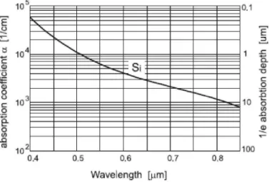
(26) 3.2. Ideal photodiode In general, a photodiodes is a solid state transducer used for converting light energy into electrical energy. The main requirements of the ideal photodiodes are: To detect all incident photons. Bandwidth is larger than the one of an input signal. To have noise immunity. The photodiodes work in the diode reverse biased zone. They work with a fix inverse bias voltage (VB) on their terminals and the photocurrent will be modulated by the incident light. The Figure 3.2 shows the photocurrent as a function of voltage for three different levels.. Figure 3.2: Characteristic curve of the photodiode.. Note that the photodiode delivers a current even when no light is available. That current is called "dark current".. 3.3. Absorption light in silicon In the process of light absorption, part of the photons is absorbed into the material. The lightintensity (I) decrease exponentially with distance into the material: (9) (3.2). Where /? is the absorption coefficient that depends upon of the wavelength (X) of silicon (10). (3.3) and A is given in micrometers [u.m].. 13.
(27) Photodiodes designed with a CMOS technology are sensitive only for a particular wavelength range. In silicon at large wavelengths, A > 9 5 0 nm, the photon energy is not high enough to create an electron-hole pair. On the other hand, for low wavelength, A < 4 0 0 nm, excess carries are generated very close to the photodiode surface. Another parameter of interest is the depth when the intensity of the light decay to / 1. incident-light. This depth is named / 1. e. e. of the. absorption depth and is equal to. Figure 3.3 shows the absorption coefficient a and / 1. absorption depth as a function of the. e. wavelength of the incident light.. 0.4. 0.5. 0.6 Wavelength. 0.7. 0,8. [j.im]. Figure 3.3: Absorption coefficient P versus wavelength.. Once the light reaches the surface, it decreases exponentially:. Now we can define G(x) as the carrier generation rate with the following equation.. Where O is the photon flux and it can be expressed as: 0. P. in. is the incident power at the surface, h is the Plank constant, v is the frequency of the. photon and r is the reflection coefficient (9).. 14.
(28) 3.3.1. An easy approach of the photocurrent p.. In order to determinate the current generated by the incident light, we can define the term -. i 2 L. hn. as the numbers of photons arrived for a given v frequency. The number of generated carrie p.. pairs is closed to p.. toije. where r\ is the quantum efficiency. Finally the photocurrent is closed. where e is the electron charge (9).. Now we define the photodiode responsivity, it is the average photocurrent per unit of incident power:. To find an equation of responsivity in terms of the wavelength use equation 3.1 and make/ = v, therefore:. Where X is in um. It is important not to lose the interest of this approach allow us to find an easy equation for the photocurrent. The photocurrent, therefore, can be obtained simply multiplying the responsivity by the incident power at the surface as follows:. Analyzing the Equation 3.9, we expect higher levels of current using higher wavelengths. But the quantum efficiency also depends on the wavelength and the semiconductor type. A typical value for the quantum efficiency in a CMOS photodiode is about 40%-70% (8). Figure 3.4 shows the responsivity as a function of the wavelength for three different semiconductors.. 15.
(29) Figure 3.4: Responsivity of Si, Ge and InGaP photodiode.. 3.4. Photodiode design To understand the structures of the different CMOS photodiodes, we need to explain the CMOS technology. Figure 3.5 shows the different layers of a CMOS technology having 0.35µm as a minimum feature size using in the design of Metal and Oxide Semiconductor Field Electric Transistors (MOSFET) (11) . The objective of this section is to describe the process of fabrications of CMOS photodiodes and transistors. In designing photodiodes, the available IC layers are the same as in CMOS transistor design.. Figure 3.5: Cross view of 0.35μm CMOS technology layers.. 16.
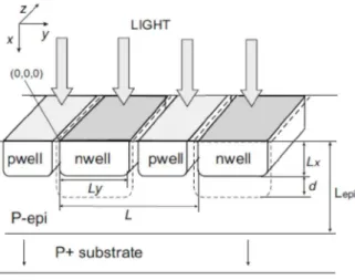
(30) 3.4.1. Photodiodes main variants A photodiode consists of a PN junction made from different layers of the CMOS technology. The alternative designs are: >. Nwell/p-substrate. >. N+/p-substrate. >. P+/nwell/p-substrate. >. P+/nwell. Two different topologies are available in a standard CMOS technology with well implantation: >. Twin-well with adjoined wells. >. Triple-well with separate wells. Basically, the fist scheme consists of two different wells to form two sort of transistors (PMOS and NMOS). The second scheme consist of one well, normally a nwell, and it is used to form the PMOS transistor. In the NMOS transistor the substrate functions as the well where the device is built. Considering the substrate, two different photodiode design schemes are available (8): > >. High resistance substrate Low resistance substrate. The low resistance substrate consists of a p+substrate under the p-epi layer, as shown in Figure 3.7 and Figure 3.10. Otherwise, the substrate is considering as "high resistance substrate". Some of these variations are shown in the Figure 3.6, Figure 3.7, Figure 3.8 and Figure 3.9.. Figure 3.6: Finger nwell/p-substrate photodiode structure with high resistance substrate and twin-wells in standard CMOS technology.. 17.
(31) Figure 3.7: Finger nwell/p photodiode structure with low-resistance substrate and twin-wells in standard CMOS technology.. Figure 3.8: A finger nwell/p-substrate photodiode structure with high resistance substrate and separate-wells standard CMOS technology.. Figure 3.9: Finger n+/p-substrate photodiode with high-resistance substrate. 18.
(32) Figure 3.10: Finger p+/nwell/p-substrate photodiode structure with low-resistance substrate and adjoined-wells.. In designing the photodiodes, L , L are selected to maximize the bandwidth. Nevertheless, y. L , d, L x. epi. are technology dependent parameters which can not be changed.. There are two main different geometries: > >. Minimal nwell/n+ width Lymin. Typically for standard CMOS, the minimal width is twice the nwell/n+ depth: Lymin=2u.m. Nwell/n+ width much larger than the nwell/n+ depth: Ly=10 u.m.. 3.5. Bandwidth of photodiodes in CMOS Inside the photodiode the carriers can move either by drift (inside the depletion region) or by diffusion (outside the depletion region). The photodiode current response is the sum of the drift current Idrift. plus the diffusion currents Idiffk. (8):. The currents of the different photodiode regions are calculated by taking the Laplace Transform of the diffusion equation in time domain (3). To obtain an estimated frequency domain behavior, the Discrete Fourier series in space domain is applied to the Laplace expression.. 3.5.1. Nwell/p-substrate, high resistance and twin well technology This section presents a frequency structure. In this case, Idiff +and n. representation of the nwell/p-substrate photodiode. Idiff +are p. zero because n+ nor p+ material are used. A. representation of this structure was presented in the Figure 3.6. The first current to find will be the nwell diffusion current Idiff. nwell. the method explained before to the diffusion equation (12): 19. . This current is found using.
(33) (3.12) Where p (t, x,y)is n. the excess minority carrier concentration inside the nwell, D is the diffusion p. coefficient of the holes in the n-doped layer and x is the lifetime of the minority-carrier. p. G(t,x,y). can be expressed as follow: (3.13). Where [1 is given by the equation 3.3 and <& (t) by the equation 3.6. 0. To solve the equation 3.12, four boundary conditions for the hole-profile are required, two in each direction, x and y. The Figure 3.11 shows those boundary conditions:. Figure 3.11: The boundary conditions for hole densities inside nwell.. Using those boundary conditions and applying Laplace Transform and Discrete Fourier series, the final expression for the nwell diffusion current is:. Applying some simplifications like in (3), the -3dB bandwidth frequency can be approximated with:. (3.15). 20.
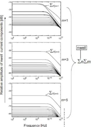
(34) L. p. is the diffusion length of the holes. Typically L is much larger than L or p. y. L , for that reason, x. the contribution of third term in brackets is very small. Equation 3.15 shows that the bandwidth can be large at higher wavelengths. But the quantum efficiency will decay if silicon is used. To develop a high speed circuit, for example in NIR range, silicon is not the best material. Perhaps Ge or InGaAsP will perform better in terms of high bandwidth and speed. The Figure 3.12 and Figure 3.13 show the amplitude and the phase as a function of the frequency for each term of the equation 3.14. The Figure 3.14 shows the result of the double sums for the amplitude and phase as a function of the frequency.. Figure 3.12: Amplitude of the double Fourier series of the nwell diffusion current for the vertical and the lateral nwell direction.. 21.
(35) 22.
(36) The next step in order to find the complete bandwidth result is to find the high-resistance substrate current. f . . J J p—subs. L. i f. ui. The substrate current is the photocurrent resulting from generated charge below wells and between them. But the contribution of generated charge below wells is dominant. Therefore, the sidewall effects are neglected. This current can be calculated by using a one-dimensional diffusion equation explained in (12):. Where n (t, x)is the excess electron concentration inside the substrate is, D is the diffusion p. n. coefficient of the electrons and x is the minority-carrier lifetime and G(t,x)is n. given by the. following equation (8):. Once again,. are given by the equation 3.3 and equation 3.6 and d is the depletion. region length (see Figure 3.6). The boundary conditions in this case are:. Lf. nt. is the depth where the light is almost completed absorbed (99%). In this case, for. X = 8 5 0 n m , Lf. nt. = 60/OTI (8).. Solving the equation 3.16 with a similar procedure like before, J. subs. can be express as:. The Figure 3.15 shows the amplitude and phase of the equation above for each term of the sum and the complete sum.. 23.
(37) Figure 3.15: Frequency response of the substrate diffusion current. Finally, the last term of the equation 3.11 has to be found. The drift current. Idrift. is directly. related to the depletion volume in which carriers are generated (8):. Where. A ffi e. at. and. A ff e. v e r. are the effective lateral and vertical depletion region areas in. comparison with the total photodiode area. A. t o t a. i.. The transit time of the holes and electrons inside depletion region is:. 24.
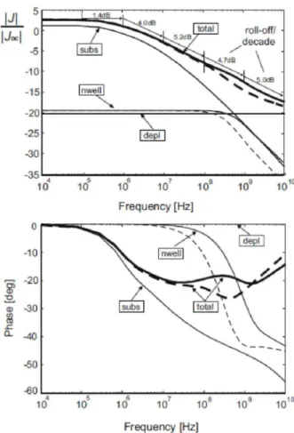
(38) Table 3.1: List of parameters.. Using equation 3.22 to equation 3.26, the cutoff frequency can be calculated as (13):. For a standard CMOS technology of 0.18u.m, f. p. = 10.S2GHz. and f. n. = 46.3GHz.. Those. frequencies are higher than the others two cutoff frequencies (see Figure 3.14 and Figure 3.15). For that reason the drift current will be taken as a constant in frequency domain. The Figure 3.16 shows the three currents as a function of the frequency and the sum of them (8). The only different between using a 10u.m nwell or 2u.m nwell is the nwell current curve. Notice that the maximal roll-off value is about 57 dB/decade for L = 10/OTI and 5.2 dB/decade for y. L. y. = 2\im. 25.
(39) Figure 3.16: The calculated total photocurrent response of nwell/p-substrate photodiode with high-resistance substrate in a twin-well technology: 2 urn (solid lines) and 10 urn nwell size (dashed lines) for \ = 850 nm.. 3.5.2. Nwell/p-substrate photodiode with low-resistance substrate and twin technology This section will analyze a photodiode with a low-resistance substrate. To keep in mind, the designers can choose between low or high resistance substrate. The section before analyze a photodiode but with high resistance substrate. The Figure 3.7 shows a representation of this photodiode. The only difference between this photodiode and the previous one is the substrate current response. Once again, this response can be found by using one-dimensional diffusion equation. But in this case, because there are two "p" layers, there will be two equations in order to describe the movement of the minority electrons:. 26.
(40) Where L. e p i. is the depth of the p-epi layer. The procedure to find the current response is the. same as the section before, but there have to be two more boundary conditions. The boundaries conditions for this problem are:. Using low resistance substrate instead high resistance will improve the bandwidth response, but the responsivity will decay. In others words, the photocurrent is lower but it can sense at higher frequencies. The Figure 3.17 shows the current response as a function of the frequency for a low resistance substrate (8).. Figure 3.17: The calculated amplitude response of nwell/p-substrate photodiode with low-resistance substrate in a twin-well technology: 2 um (solid lines) and 10 um nwell size (dashed lines) for X = 850 nm.. 27.
(41) The roll-off behavior in this case is 1-2 db/decade lower than in the previous section. Radovanovic et al, used a semiconductor parameter analyzer (SPA) HP4146B to provide the supply and bias voltage. With the SPA sensed the DC photocurrent and the frequency response of the same photodiode (Nwell/p-substrate, low-resisntance substrate, twin technology). The Figure 3.18 shows the DC behaviour and the Figure 3.19 the frequency response (8). 10-. 4. < a> '.. ~. £ id. 5. o. CL. o. Q. average input optical power [dBm]. Figure 3.18: The measured DC photocurrent of nwell/p-substrate photodiode for \ = 850 nm.. Figure 3.19: The measured (line) and calculated (dashed) responses of a nwell/p-substrate photodiode with 2 nm nwell-size,. 3.5.3. Nwell/p-substrate photodiode with high-resistance substrate and separated wells This section and the next one have a particular interest because these kind of photodiodes can be designed at LabMEMS (laboratory of micro-electromechanical systems) at ITESM, Monterrey Campus, place where I did all my investigations and simulations. CMOS of 0.35u.m technology. 28.
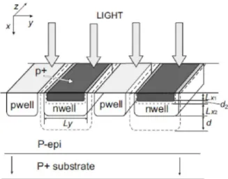
(42) with separated wells and high-resistance substrate is available there, this technology was presented before by Figure 3.5. This photodiode structure is shown in the Figure 3.8. The lateral depletion region between nwells in significantly increased. For that reason, the amplitude of the drift current response is higher. But at higher frequencies, this photodiode's roll-off is 1-2dB lower than the one with twin well technology. The Figure 3.20 shows the frequency response of this photodiode (8).. Frequency [Hz]. Figure 3.20: The response of nwell/p-substrate photodiode with high-resistance substrate in a separate-wells technology: 2 um (solid lines) and 10 um nwell size (dashed lines) for X = 850 nm. 3.5.4. N+/p-substrate with high-resistance substrate and separated wells. This photodiode structure is shown in the Figure 3.9. The response of the n+ region is obtained by changing the values of the diffusion length L and diffusion coefficient D . p. n. The maximum frequency response is determinate mainly by the depth of the n+ region. Since this depth is much smaller than the nwell one, the bandwidth will be smaller (8).. 3.5.5. P+/Nwell/p-substrate with low-resistance substrate and adjoined wells. This kind of photodiode is formed by two photodiodes: p+/nwell and nwell/p-substrate. The structure of this photodiode is shown in the Figure 3.10. Because of its structure, this kind of photodiodes is often referred as double photodiode. For this problem, first the p+/nwell junction has to be solved. To find an expression to the current, the same equation for nwell/p-substrate, only changing the values of the diffusion coefficients, diffusion lengths and junction depth is used. The boundary conditions for the "second" photodiode (nwell/p-substrate) are shown in the Figure 3.21.. 29.
(43) Figure 3.21: The boundary conditions for the hole density inside the nwell for the double-photodiode.. The total response at the frequency of this photodiode is shown in the Figure 3.22.. F r e q u e n c y [Hz]. Figure 3.22: The response of p+/nwell/p-substrate photodiode with lowresistance substrate in an adjoined-wells technology: 2 nm (solid lines) and 10 urn nwell size (dashed lines) for \ = 850 nm. The bandwidth of this photodiode is higher than the nwell/p-substrate photodiode, but the responsivity is lower. That means that the photocurrent will be lower and the circuit connected to amplify the current has objectives more difficult to reach.. 3.6. Scope and limitations of CMOS photodiodes This section discuses CMOS photodiodes considering the wavelength range, bandwidth and the impedance needed to have a good impedance match to the amplifier.. 30.
(44) 3.6.1. Wavelength limitations CMOS photodiodes work when the incident light has a wavelength between 400nm to l u m . This range includes the visible spectrum (400nm-700nm) and part of the near infrared spectrum (700nm-2.5u.rn). CMOS photodiodes fit very well for APS and others applications related to image capture and digital communications. Some of these applications are listed below. >. 10 Gigabit/sec fiber Ethernet: A=850nm.. >. CD players and recorders: A=750nm.. >. DVD players and recorders: X=650nm.. >. DVD - blue ray disc: X=400nm.. 3.6.2. Bandwidth and responsivity comparison A nwell/p-substrate and a p+/nwell/p-substrate photodiode are compared. For comparison, the wavelength used was A.=850nm. The Table 3.2 and Table 3.3 show the important parameters for nwell/p-substrate and P+/nwell/p-substrate of all variants. The responsivity is normalized with respect of the responsivity of the low resistance in all the cases. The nwell/p-substrate with high resistance has the best responsivity. The results can demonstrate that the second photodiode (p+/nwell/p-substrate) is much better than the first one (nwell/p-substrate) in terms of bandwidth. Note that the cut-off frequency is higher for low resistance substrate. Table 3.2: Cut-off frequency and responsivity for nwell/p-substrate photodiode.. Nwell/p-substrate High resistance. Low resistance. Separated wells Ly= 2 u.m Ly = 10|um. Adjoined wells Ly= 2 um Ly = 10|um. Cut-off frequency. 1MHz. 1MHz. 0.6MHz. 0.6MHz. Average roll-off/dec. 4.6. 4.9. 4.3. 4.8. Responsivity. 3dB. 3dB. 3dB. 3dB. Cut-off frequency. 1.4MHz. 1.4MHz. 1MHz. 1MHz. Average roll-off/dec. 3.9. 4.2. 3.9. 4.4. Responsivity. 0dB. 0dB. 0dB. 0dB. 31.
(45) Table 3.3: Cut-off frequency and responsivity for p+/nwell/p-substrate photodiode.. P+/Nwell/p-substrate High resistance. Low resistance. Cut-off frequency. Separated wells. Adjoined wells. Ly= 2 um. Ly = 10u.m. Ly= 2 um. Ly = 10um. 1.6MHz. 1.6MHz. 1.2MHz. 1.2MHz. Average roll-off/dec. 3.9. 3.9. 3.9. 4. Responsivity. 3dB. 3dB. 3dB. 3dB. Cut-off frequency. 2MHz. 2MHz. 1.8MHz. 1.8MHz. Average roll-off/dec. 3.3. 3.3. 3.1. 3.15. Responsivity. OdB. OdB. OdB. OdB. The next list shows the different photodiodes in order of their speed starting from the fastest one. 1.. P+/nwell/p-substrate, separated wells, low resistance. 2.. P+/nwell/p-substrate, adjoined wells, low resistance. 3.. P+/nwell/p-substrate, separated wells, high resistance. 4.. Nwell/p-substrate, separated wells, low resistance. 5.. P+/nwell/p-substrate, adjoined wells, high resistance. 6.. Nwell/p-substrate, adjoined wells, low resistance. 7.. Nwell/p-substrate, separated wells, high resistance. 8.. Nwell/p-substrate, adjoined wells, high resistance. A spatially modulated photodiode can be designed (3). With this technique, is possible to have a nwell/p-substrate photodiode as fast as a p+/nwell/p-substrate one sacrificing responsivity. To analyze the responsivity, it can be seen as a function of the frequency using the following equation (8).. This is valid only for frequencies higher than the cut-off frequency.. 32.
(46) 3.6.3. Parasites comparison The input impedance of the amplifier that is connected to the photodiode can be calculated from the parasites of the photodiode. The parasite that influences more in the input impedance is the parasitic capacitance. This capacitance can be extracted from the photodiode design. Once the capacitance is obtained, the input impedance can be calculated as a function of the cut-off frequency desire.. The Table 3.4 shows the parasitic capacitance and the in impedance that has to be designed by the amplifier to reach 3GHz bandwidth. Table 3.4: Parasitic capacitance and in impedance for different photodiodes.. To illustrate the use of the last table, the Figure 3.23 shows a photodiode equivalent circuit (14).. Figure 3.23: Photodiode equivalent circuit. The parasitic capacitances and the input impedance shown in the Table 3.4 are Cj and R of the L. equivalent circuit. The R. sh. and R resistance are parasites that can be extracted from the s. photodiode layout.. 33.
(47) Chapter 4 Simulation and design of an optoelectronic interface. The first part of this chapter shows the three designed designed: p+/nwell, nwell/p-substrate, n+/p-substrate. A spatially modulated technique was applied to the three photodiodes. Moreover, in order to fabricate the integrated circuit, the ring pad was included too. The second part of this chapter shows the designed high bandwidth amplifier. The amplifier consists on five blocks: Transimpedance amplifier (TIA), Inductive Peaking, CMOS Inverter, Source degeneration and CMOS Inverter Amplifier.. 34.
(48) 4.1. P+/nwell photodiode design in a 0.35μm CMOS technology This section shows the p+/nwell design. The design was a replica of the photodiode described in (2) but with the technology advisable here. The pwell could not be including in the design because of the technology. Instead of using the pwell layer, it is using the substrate. Figure 4.1 shows the design of the p+/nwell photodiode. The size of the photodiode is around 148µmx148µm.. MET2. NTUB. PPLUS. MET1. Figure 4.1: P+/nwell photodiode.. The layers used in this design are:. NTUB (nwell) DIFF (diffusion) NPLUS (n+) PPLUS (p+) CONT (contacts MET1 to DIFF) MET1 (metal 1) VIA1 (contacts between metal 1 and metal 2) MET2 (metal 2) 35.
(49) 4.1.1. Designed blocks The designed blocks are designs advisable in the technology library. Actually, these designs can be seen as the “union” of specific layers in a specific form to warranty the success of the Design Rule Check (DRC) test. For example, the via pdm1 has four layers: PPLUS, MET1, CONT and DIFF. For the design of the p+/nwell photodiode, four designed blocks were used: Via: pdm1 (via from p+ to metal 1) o PPLUS o MET1 o CONT o DIFF Via: m1m2 (via from metal 1 to metal 2) o MET1 o MET2 o VIA1 Guard Band: pdsub (guard band with p+) o PPLUS o CONT o MET1 o DIFF Guard Band: ndnwell (guard band with n+ and nwell) o NTUB o NPLUS o CONT o DIFF o MET1. 4.1.2. Node designs of the p+/nwell photodiode To make the correct node designs, is important to visualize the p-node (PNODE) and the n-node (NNODE) of the photodiode. For this photodiode, the signal of the PNODE is taken from the p+ structure. The signal of the NNODE is taken from the nwell. The first node to design is the PPNODE. Figure 4.2 shows the p+ fingers with a via to metal 1. The others layers were occulted except NTUB. The size of the fingers is 92μmx1μm. The width of the via is 15μm.. 36.
(50) PPLUS. NTUB. Figure 4.2: P+ fingers of p+/nwell photodiode.. To have the signal in metal 2, is necessary put a via from metal 1 to metal 2 (via: ,1m2). Figure 4.3 shows the PNODE with all the layers. MET2. Figure 4.3: Pnode connection of p+/nwell photodiode.. The procedure to design the PNODE is: 1. Create a p+ finger and copy many times as wanted. This photodiode has 19 p+ fingers. 2. Create a via from p+ to metal 1 (via:pdm1) and copy it. 3. Create a via from metal 1 to metal 2 (via:m1m2) and copy it. Create a NTUB rectangle with sizes higher than the p+ fingers structure. The NTUB rectangle can be designed after or before the PNODE, in this case was designed before. To obtain the signal from the nwell, this step has to be done.. 37.
(51) To obtain the signal from the nwell, another designed block was used. A Guard Band of ndnwell is used to extract the signal to metal 1. This type of Band Guard is commonly used to keep the structure inside of it out of noise. Once the signal is in metal 1, a via from metal 1 to metal 2 is used again. Figure 4.4 shows the NNODE connection of the p+/nwell photodiode. Note that the p+ fingers do not have connection to metal 2. PPLUS MET2. Figure 4.4: Nnode connection of p+/nwell photodiode.. The procedure to design the NNODE is the same as the PNODE only with one difference. Instead of using a via from p+ to metal 1, a guard band is used to take the signal to metal 1.. 4.1.3. Guard bands design Two guard band rings are used to keep the photodiode out of noise. The guard bands used was described before. The type of the internal ring guard band is ndnwell and the external is pdsub. Figure 4.5 shows the two guard bands. The internal guard band has to be connected to VDD and the external one to GROUND. To make the connection to VDD a via from metal 1 to metal 2 was used. It is necessary because both guard bands has metal 1. Figure 4.6 shows the connection of the internal ring to VDD.. 38.
(52) NTUB Internal ring External ring. Figure 4.5: Guard bands of p+/nwell photodiode.. Figure 4.6: Internal ring connection.. 4.2. Nwell/p-substrate photodiode design This section shows the design of a nwell/p-substrate photodiode. A 0.35μm CMOS technology was used. The size of this photodiode is around 68µmx68µm. Figure 4.7 shows the entire photodiode design.. 39.
(53) MET2. NTUB. Figure 4.7: Nwell/p-substrate photodiode.. 4.2.1. Node designs of the nwell/p-substrate photodiode. The design of this photodiode was done without using designed blocks. The first block to design was de NNODE. Figure 4.8 shows the NTUB and DIFF layers of the NNODE connection. NTUB DIFF. Figure 4.8: NTUB+DIFF layers of the Nnode connection.. The size of the DIFF rectangles is 2.6μmx5μm. To pass the DRC, the DIFF area has to be inside the NTUB.. 40.
(54) Figure 4.9 shows the NTUB, DIFF and CONT layers of the NNODE connection. To pass the DRC, the size of the contacts has to be 0.4μmx0.4μm. The contacts are used to connect the Nwell to metal 1.. CONT. Figure 4.9: NTUB+DIFF+CONT layers of the Nnode connection.. Figure 4.10 shows the NTUB, DIFF, CONT and MET1 layers of the NNODE connection.. MET1. Figure 4.10: NTUB+DIFF+CONT+MET1 layers of the Nnode connection.. After putting the metal1 layer, a via from metal 1 to metal 2 was used. Figure 4.11 shows the NNODE connection with all the layers.. 41.
(55) Figure 4.11: NNODE connection of nwell/p-substrate.. The design of the PNODE needs the DIFF, CONT and MET1 layers. Also a via from metal 1 to metal 2 is needed. Figure 4.12 shows the DIFF and CONT layers of the PNODE. DIFF CONT. Figure 4.12: Pnode connection of nwell/p-substrate.. Only one guard band was designed for this photodiode to avoid noise. This guard band is connected to ground.. 4.3. N+/p-substrate photodiode design The procedure design of this kind of photodiode is the same as the nwell/p-substrate photodiode. Two simple changes were made. Figure 4.13 shows the n+/p-substrate photodiode. Instead of using the NTUB layer to make the fingers, I used the NPLUS layer.. 42.
(56) Instead of making the way the NNODE by putting the DIFF and CONT layers, I used a designed block. The one needed was a VIA from n+ to metal 1 (VIA: ndm1) NPLUS. MET2. Figure 4.13: N+/p-substrate photodiode.. 4.4. Spatially modulated photodiode designs Once the nwell/p-substrate and the n+/p-substrate were designed, a metal 3 fingers were added to obtain the effect described in (3). Figure 4.14 and Figure 4.15 show those designs.. MET3. Figure 4.14: A Nwell/P-substrate spatially modulated photodiode in 0.35µm CMOS technology.. 43.
(57) Figure 4.15: A N+/P-substrate spatially modulated photodiode in 0.35μm CMOS technology.. 4.5. Ring design Once the layout design was made, the next block to design is the ring. This is essential to do in order to fabricate an integrated circuit. The ring has the pads needed to capture the signal from the outside. The designer can see the ring as an external design that doesn’t depends on the circuits or elements designed before, but this is not truth. The size of the ring, the numbers of pads, and the types of the pads depends on the circuit design. But once the designer knows all those things, the ring can be designed separately from the circuit. I decided to design three different photodiodes and them in the same integrated circuit. The three photodiodes are a p+/nwell, n+/p-substrate and nwell/p-substrate. For the first one, two outputs terminal (NNODE and PNODE) and two others for the band guards rings are needed. The last two are the voltage and ground terminals. The second one and the third one have two terminal each other (NNODE and PNODE again) and the just ground terminal is needed for the band guard ring. The ring, in this case, has to have 6 outputs terminal, one voltage terminal and one ground terminal. With this in mind and considering the size of the three photodiodes, the ring was designed. The Figure 4.16 shows the ring design made for the three photodiodes.. 44.
(58) Voltage pad. Outputs pads. Outputs pads. Ground pad Figure 4.16: Ring design.. All the pads are designed blocks and they can be found in the technology libraries. For the technology used, those pads are called as follow. AVDD3ALLP AGND3ALLP APRIOP Notice that the ring has others designed blocks to encapsulate all the circuit. The others designed blocks are called: CORNERP PERI_SPACER_50_P PERI_SPACER_100_P Once the ring and the desire photodiodes were designed, it can easily incorporate both circuits into a third one. This is very helpfully for the designer for the design rule check revision. The Figure 4.17 shows the entire circuit with the ring designed.. 45.
(59) N+/p-substrate photodiode. P+/nwell photodiode. Nwell/p-substrate photodiode. Figure 4.17: Photodiodes with ring.. 4.6. High bandwidth amplifier design Figure 4.18 shows the block diagram of the proposal amplifier. This design offered a great bandwidth but the stability is not good because of the lack of a closed-loop system. This system was designed using a 0.35µm CMOS Technology.. Figure 4.18: Block diagram of a high bandwidth amplifier.. 46.
(60) The blocks of the amplifier are: VCCS (Voltage controller, current source). COMMON_SOURCE_REAL1. THRESHOLD_CURRENT_REFERENCE1. INDUCTIVE_PEAKING_NMOS_REAL1. CMOS_INVERTER1. SOURCE_DEGENERATION_REAL1. The current range was obtained from the Figure 3.18. The minimum current is 2u.A and the maximum current is 40u.A. The VCCS is used to simulate the photocurrent. The transadmitance was set at 1S (1 siemens) in order to convert a voltage source into a current level. The others blocks are explained in more details later. Three kinds of analysis were realized using this circuit, a dc analysis, ac analysis and a transient analysis.. 4.6.1. Transimpedance amplifier The goal of the TIA is to change the current level into a voltage level. The transfer function ( ^ H L ) of this block has resistive dimensions (Q), for that reason they are called "transimpendance amplifiers". The Figure. shows the schematic representation and idealized model of these. amplifiers.. Figure 4.20: Schematic representation and ideal model of the transimpedance amplifier.. This block can be done with a few transistors and resistors. Figure 4.21 and Figure 4.22 show two designs of a TIA(15).. 47.
(61) Figure 4.21: Common-Gate circuit as a transimpedance amplifier. Figure 4.22: Improved circuit for transimpedance amplifier. Figure 4.23 shows a common source circuit using as a TIA. This design is much simpler; only consist in a transistor, a resistor and a current source.. Figure 4.23: Common source as a transimpedance amplifier. 48.
(62) R is the combined output resistance of M 1 and M 2 . 0. Common source topology for a TIA is used in the high bandwidth amplifier. Two considerations were made to select the R value of this amplifier, the output swing voltage and the highest expected photocurrent. Figure 4.24 shows the circuit capture of the TIA.. Figure 4.24: TIA design.. The output swing voltage wants to be equal to 100mV and the highest expected current is. The dimensions of the transistors and the bias current were select to have good input impedance.. 49.
(63) Using those parameters, the R. in. andR. 0Ut. are:. The simulation test proves that using a 3KQ resistor, the output voltage swing will be 105mV. The R. in. andR. 0Ut. are:. 4.6.2. Current source To design the 200uA current source, a threshold current reference topology was used. Figure 4.25 shows the schematic design.. Figure 4.25: Threshold current reference.. The only design parameter in the threshold current reference is the resistor R2. The others parameters maintain the two transistors in saturation region. The R2 resistor is calculated dividing the V voltage by the l T. bias. current (200u.A).. Simulating with that value, the current was higher than expected. For that reason, the resistor used was:. 50.
(64) 4.6.3. Analog equalizer The goal of this block is to compensate the photodiode frequency behavior to increase the bandwidth. A source degeneration circuit is proposed for this block. Figure 4.26 shows the schematic of the analog equalizer.. Figure 4.26: Analog equalizer.. The circuit consists in four high-pass filters. Each high-pass filter has different cut-off frequency in order to emphasize a particular bandwidth. Making R = R , the resistors and capacitance can be designed as follow: D. s. 1. Define the bandwidth to be emphasized (f. min. 2.. —f. max. ).. Define the numbers filters (N) to be designed.. 3. Define the gradient in decibels (AdB) between each filter. 4.. Find each cut-frequency, resistance and capacitance given by the following equations:. 51.
(65) The first high-pass filter of the analog equalizer is implemented by an active inductor. Figure 4.27 shows the schematic of the inductive peaking proposed (16).. Figure 4.27: Inductive peaking schematic.. Figure 4.28 shows the schematic capture of the inductive peaking.. Figure 4.28: Inductive peaking design.. Using the procedure explained the resistor and capacitance values are shown in the Table 4.1. AdB. = 3.75. N = 4. 52.
(66) Table 4.1: Capacitances and resistances of the source degeneration circuit.. n. R (£l). fn(Hz). n. Cn(pF). 1. 12964.727. 1,000,000. 12.2759965. 2. 8419.05556. 5,623,413. 3.36168299. 3 4. 5467.18004. 31,622,777. 0.92056987. 3550.28629. 177,827,941. 0.25209066. All the resistance and capacitance values were found. To obtain the size of the transistors, simulations of the previous block and others considerations was realized. The first step is to know the input voltage range. The voltage range was obtained by simulating the common source circuit explained before.. The voltage to calculate the size of the transistor M 2 is the average voltage expected at the input (710mV). With that value, the average current expected can be calculated applying the saturated current equation.. Using (—] = &. , the current will be 246u.A. That current is used to calculate the channel. \Lj. 0.3511'. 2. K. conductance parameter of the transistor M l , g. m. The value of g. m 1. .. 1. has one restriction because of the inductive peaking behavior. As is explained. in (16), in order to have an inductive behavior, the pole of the transfer function has to be higher than the zero.. 53.
(67) Where the values of R and C is taken from the first row of the Table 4.1. In fact, the 1. 1. capacitance C has to be added to capacitance C of the transistor M l but this capacitance is 1. gs. much smaller than C , for that reason is neglected. 1. Using. the channel conductance will give 1.9mS. The size of the transistor M 1. could be much lower, but with this value the output swing reach almost 100mV, the same as the input. To maintain the same sloop relation, a C M O S inverter was introduce between the inductive peaking and the source degeneration. Figure 4.29 shows the schematic capture of the CMOS inverter used.. Figure 4.29: CMOS inverter design.. The objective of this block is to invert the signal because the next block needs other range of voltage. The input swing voltage of this block is from 2.23V to 2.14V. To invert the signal and have a good output swing is necessary that the switching voltage would be high (17).. 54.
(68) Where E is the critical electric field of the NMOS or PMOS and are constants according to the c. technology used. Using W = 2 and W = 15, the switching voltage is 1.86V, near from the N. P. input voltage range. To certify that the behavior wished is realized by the CMOS inverter, it was necessary to simulate and to prove some sizes of the transistors. To find the size of the transistor, it was necessary simulate the previous blocks. Figure 4.30 shows the schematic capture of the source degeneration.. Figure 4.30: Source degeneration circuit.. This block can be seen as a resistive load inverter and the switching voltage can be calculated by equating the two currents (17). Using. = 7000, the switching voltage can be calculated solving the. quadratic equation showed.. This value is low enough to get the desire behavior at the output.. 55.
(69) 4.6.4. Voltage amplifier The second CMOS inverter is used to have at the output a non-inverter signal referring to the photocurrent. That means that until higher is the photocurrent, higher will be the voltage at the output and not vice versa. The other goal of this inverter is to have the best output swing voltage. The procedure to design this CMOS inverter is the same as the first one. But in this one, is more critical to have the switching voltage very near to the input voltage range. The input voltage range in this case is from 2.35V to 2.26V and the switching voltage using W = 1 and W = 50 N. P. is 2.35V. The Figure 4.31 shows the schematic capture of the last CMOS inverter.. Figure 4.31: Voltage amplifier.. The Table 4.2 shows the voltages ranges and the switching voltage at the last three blocks. Table 4.2: Voltage ranges.. 4.6.5. Simulation results A DC analysis was realized to verifying the output swing in each block. The most important is the output of the entire system. The Figure 4.32 shows the DC analysis using a DC voltage source from 2uV to 40uV to simulate the photocurrent range.. 56.
(70) From top to bottom of the Figure 4.32, the curves shown are: . TIA output (TIA). Inductive peaking output (PEAKING). The first CMOS inverter output (INVERTER1). The source degeneration output (EQUALIZADOR). The second CMOS inverter output (INVERTER2).. Figure 4.32: DC analysis. Three measurements are shown by each curve. The voltage when the current is 0A, 2µA and 40µA. The Table 4.3 shows these simulation tests. Table 4.3: DC analysis results.. Input current (µA) 0 2 40. TIA (mV) 657.37 662.66 762.57. PEAKING (V) 2.2378 2.2331 2.1454. INVERTER1 (mV) 203.93 208.90 321.95. 57. EQUALIZER (V) 2.3518 2.3481 2.2639. INVERTER2 (V) 1.1399 1.2107 3.0069.
(71) From table 4.3, the transimpedance parameter can be calculated as 47 ^ / ^ . m. An AC analysis was done to calculate the bandwidth of the system. In this case two curves were shown in the Figure 4.33, one is the voltage gain in decibels at the TIA output and the second one is the voltage gain at the output of the amplifier. The real gain of the system will be the subtraction of the two gains shown.. Figure 4.33: AC analysis.. A strange behavior is presented in the AC analysis seen in the output of the system (INVERTER2). That peak is done by the inductive peaking and source degeneration block. This topology explained in (8) is used because the bandwidth behavior of the photodiode. This simulation does not have considering the frequency photodiode response. In order to have a real behavior of the entire system (photodiode and amplifier) it is necessary to find a way to estimate the frequency response. Three measurements are important in an AC analysis, the frequency bandwidth, gainbandwidth and the gain. From the last figure, the frequency bandwidth is 852MHz; the gainbandwidth is around 2GHz and the gain is 22dB. 58.
(72) The last analysis is a transient analysis. This was done by having a voltage source changing its values at different times. The Figure 4.34 shows two curves: First, the input that changes its values from 0V to 2µV, 40µV and 21µV (mention a voltage level or current level is the same because the use of the VCCS) and second, the curve of the output of the system (INVERTER2).. Figure 4.34: Transient analysis.. The DC values of the second curve are almost the same as illustrated Table 4.3. The characteristic transient analysis is shown by the Figure 4.35. The time needed by the output to change from 1.07V to 2.93V is 295.7ns.. Figure 4.35: A closed view of the transient analysis.. 59.
(73) Chapter 5 Conclusions and futures work. This thesis has been developed to support the BioMEMS research group that is working on several projects related to optoelectronic interfaces for spectrophotometers.. 5.1.. Conclusions. My own conclusions are listed below. It is possible to design CMOS photodiodes to work in the visible range and part of the NIR spectrum. Spatially modulated photodiodes can be implemented in CMOS technology in order to increase the bandwidth. Unfortunately, this technique reduces the responsivity. For the applications where the wavelength. range is higher than 1u.m, silicon. photodiodes are not suitable. For this wavelengths range, GaAs or other special materials have to be used. These special materials are essential to monitor some physiological variables like glucose concentration.. 60.
(74) >. In this thesis, I have used 0.35u.m CMOS which is a low cost technology. We can use 0.18um technologies for future works, especially if we want to incorporate digital circuits to the interface.. 5.2.. Future works. A list of the future research lines are: The characterization of the different photodiodes. This can be done in two ways. o. Create modules using HDL (hardware description language) and incorporate them in the simulator. This strategy allows to perform a simulation of the complete system.. o. Using the PEX (Parasite extraction) module. This module allows to extract the parasite elements and to build a schematic circuit. This circuit can be used to simulate the photodiode behavior.. A physical realization of the photodiode. Even if the amplifier is not included in the chip, the photodiodes can be fabricated and tested using external amplifiers. The design of a closed-loop circuit to amplify the photocurrent. Figure 5.1 shows a topology that can be used in applications where a high bandwidth circuit is not needed (18).. "CM. I Figure 5.1: Input current instrumental amplifier.. 61.
(75) Bibliography [I] Philippe Lalanne and Jean-Claude Rodier, "CMOS photodiodes based on vertical p-n-p junctions," Institut d'Optique Theorique et Appliquee. [2] Yu-Wei Chang, Ping-Chun Yu, Yang-Tung Huang, Yuh-Shyong Yang, "A High-Sensitivity CMOS-Compatible Biosensing System Based on Absorption Photometry," Sensors Journal, vol. 9, pp. 120-127, Febrary 2009. [3] Jan Genoe, Danniel Coppee, Johan Stiens, Roger Vounckx, M . Kuijk, "Calculation of the Current Response of the Spatially Modulated Light CMOS Detector," Transactions on electron devices, vol. 48, pp. 1892-1902, Sept. 2001. [4] Chen Xu, Wing-Hung Ki, Mansun Chan, "A Low-Voltage CMOS Complementary Active Pixel Sensor (CAPS) Fabricated Using a 0.25um CMOS Technology," Electron Device Letters, vol 23, pp. 398-400, July 2002. [5] Alexander Fish, Shy Hamami, Yadid-Pecht, "Self-powered active pizel sensors for ultra-lowpower applications," Circuits and systems, vol. 5, pp. 5310 - 5313, May 2005. [6] Markus Grozing, Michael Jutzi, Winfried Nanz, Manfred Berroth, "A 2 Gbit/s 0.18 u.m CMOS Front-End Amplifier for Integrated Differential Photodiodes," Silicon Monolithic. Integrated. Circuits in RF Systems, pp. 4, Jan 2006. [7] Tatsushi Nakahara, Hiroyuki Tsuda, Kouta Tateno, Shinji Matsuo, and Takashi Kurokawa, "Hybrid Integration of Smart Pixels by Using Polyimide Bonding: Demonstration of a GaAs pi-n Photodiode/CMOS Receiver," Selected topics in quantum electronics, vol. 5, pp. 209-216, March 1999. [8] Sasa Radovanovic, Anne-Johan Annema, Bram Nauta, "High-Speed Phodiodes in Standard CMOS Technology," Springer, 2006. [9] W. Etten, J. Plaats, "Fundamentals of Optical Fiber Communications," Prentice-Hall, 1991. [10] Wei-Jean Liu, Oscal T. C. Chen, Li-Kuo Dai, Ping-Kuo Weng, Kaung-Hsin Huang, Far-Wen Jih, "A CMOS photodiode model," Behavioral Modeling and Simulations,. pp. 102 - 105, Oct.. 2001. [II]. Austria Microsystems, "0.35um CMOS C35 Process Parameters," Vols. ENG - 182, 2007.. 62.
(76) [12] S. M . Sze, "Physics of semiconductor devices," Wiley-Interscience, [13] Stephen B. Alexander, "Optical communication receiver design,". 2. nd. Edition.. Telecommunications. Series, vol 37, 1997. [14] Hamamatsu, "Photodiode technical information" [15] Behzad Razavi, "Design of Analog CMOS Integrated Circuit," McGraw Hill, 2001. [16] Chap-Hsin Lu, Wei-Zen Chen, "Bandwidth enhancement techniques for transimpedance amplifier in CMOS technologie," Solid-State Circuits Conference, pp. 174-177, Sept. 2001. [17] David Hodges, Horace Jackson, Resve Saleh, "Analysis and Design of Digital Integrated Circuits in Deep Submicron Technology," MacGraw-Hill,. 2003.. [18] Sergio Franco, "Design with Operational Amplifiers and Analog Integrated Circuits," McGraw Hill, Third Edition, 2005.. 63.
(77)
Figure


+7


Documento similar
fluorescent dyes) for in vivo imaging of living tissues are: i) permeation of a substrate is not required, making non-invasive techniques for in vivo monitoring of ROS/redox
Figure 3: Relationship between the response variables (productivity, density and recent population trends of the Bonelli’s eagle) and the predictor environmental variables in the
Considering the three domains of the 23-Sn substrate and two equivalent molecular adsorption geometries within one substrate domain, a total of six orientations
classified by a color code.. 172 The resolution in Figure 3 23 is so good that we have tried to determine the exact atomic position of all the atoms in the graphene substrate
According to the local coupling with the substrate, we find areas with markedly different adsorption, dissociation and diffusion pathways for both molecular and
X, Y, and Z-components of the surface displacement and traction fields for loads with magnitudes of 15%, 10% and 5% of the substrate Young ’s modulus, aligned with the X
The distribution in plant, substrate and leachate of PBZ applied to containerized oleander seedlings were studied after a single liquid drench application to the substrate surface
Figure 4 shows changes in the friction coefficient of the substrate and the coatings, according to the sliding distance, where the steady state is clearly seen. During this state
