A Hands-On Education Project: Antenna
Design for Inter-CubeSat Communications
Ramón Martínez Rodríguez-Osorio and Enrique Fueyo Ramirez
Abstract
CubeSat platforms have become a de facto standard for universities willing to initiate space-technology activities with students. These small satellite platforms ease the implementation of hands-on education projects and opening the apertures of new research areas. Moreover, due to the limited volume (a 10 cm cube) and power (1 W), the application of imaginative solutions is mandatory. This leads to new innovation processes in the course of CubeSat projects. In this paper, we present a hands-on education project the aim of which is the specification, design, building and measurement of an antenna for communication between nanosatellites and, in particular, CubeSats. The project lies within the framework of ETSIT-UPM innovative education activities in the area of space technology, where students play a leading role in real engineering projects.
Keywords: Antenna arrays; beam steering; formation flying; electrical engineering education; inter-satellite communications; satellite communications; patch antennas; satellite antennas; small satellites; CubeSat
1. Introduction
A
CubeSat picosatellite is a small satellite with a cubicalform, with a side dimension of 10 cm and with a maxi-mum mass of 1 kg. The CubeSate was conceived in the late
1990s by Prof. Robert Twiggs and Prof. Jordi Puig-Suari to bring space technology to engineering students, willing to develop a satellite by their own means with a reduced cost and in a two-to-three-year period [1]. CubeSats are usually built from commercial off-the-shelf components, and are launched into low Earth orbits (LEO) using special "deployers," such as the Poly-PicoSatellite Orbital Deployer (P-POD). This leads to stringent weight, power, and geometry constraints. CubeSats are either launched in multiples in medium-capacity launchers, or "piggyback," using the excess capacity of heavy launch vehicles.
CubeSat projects have become a de facto standard in the universities, providing space technology degree programs with a real satellite platform that facilitates access to space, thanks to its rapid development cycle and reduced cost. The specifi-cations to build a CubeSat can be found in [2]. This document defined the specifications of the basic CubeSat unit (denoted as "1U") as a cube of 10 cm x 10 cm x 10 cm. CubeSats are scalable platforms, the most common versions of which are
denoted as "2TJ" (10 cm x 10 cm x 20 cm) and "3TJ" (10 cm x 10 cm x 30 cm).
Since the conception, CubeSat projects have multiplied in many universities worldwide as a means of innovative edu-cation, promoting hands-on projects between students. From a learning perspective, CubeSat projects join students with diverse backgrounds that work together to reach a common objective.
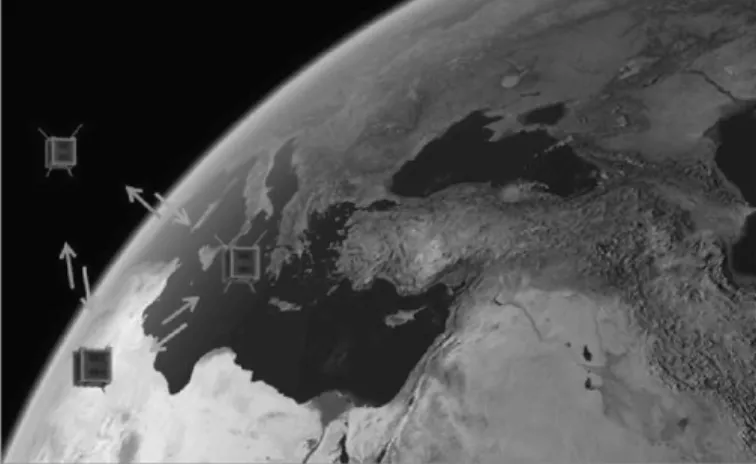
with the design of an antenna system for inter-satellite com-munications applicable to CubeSat missions. Up to now, CubeSat missions have been based on the use of a single sat-ellite, which offers limited performance and does not require a complex inter-satellite communication subsystem. The project was motivated by the upcoming satellite distributed and for-mation-flying missions that will be launched in the next years. Figure 1 shows the concept of a distributed CubeSat mission, where three satellites share information to cooperate and coor-dinate operations.
QB50 is one of the nanosatellite missions that might bene-fit from inter-satellite communications. QB50 aims at launching a cluster of 50 nanosatellites under the 2U CubeSat standard. The scientific objectives of QB50 are the in-situ measurements of the spatial and temporal variations in the composition of the lower thermosphere, and the study of the reentry process. The 50 CubeSats will be sequentially deployed from a Shtil-2.1 launcher in 1200 seconds, at an initial altitude of 320 km [4], The mission lifetime is around 90 days. It is expected that the spacecraft will be located in a cluster with slowly increasing distances until reentry, at an altitude of 90 km. The QB50 mission is thus particularly suited to test inter-satellite links.
Similar to QB50, the Armada [5] and HiDEF (High-Lati-tude Dynamic E-Field) Explorer [6] missions propose the use of large CubeSat constellations for the study of small-scale plasma physics in the ionosphere/thermosphere, and meas-urements of how energy transfers from magnetosphere into the thermosphere-ionosphere region, respectively. Other nanosa-tellite missions - such as HUMS AT, with an objective of the implementation of a short-messaging communication service for connecting a set of users with worldwide distributed sen-sors with humanitarian applications (climate and pollution monitoring, contamination measurements, etc.) - might benefit from the use of inter-satellite links in order to (for example) reduce communication delay and provide redundancy [7],
CubeSat clusters have also been proposed as a means to share and distribute memory, communications, and processing resources in interplanetary missions that require heavy proc-essing. This concept requires the setup of high-speed inter-satellite links to generate the backbone network [8]. Forma-tion-flying missions currently proposed by space agencies mean a technological breakthrough in the area of science and observation missions. In these missions, several spacecraft are coordinated to maintain a desired relative separation, orienta-tion, or position [9]. Compared to large monolithic single-sat-ellite missions, the use of small, low-mass satsingle-sat-ellites reduces risk, and launch and mission costs. Distributed-satellite mis-sions can share resources, the system is more tolerant against errors and component failure, and the availability is higher than in centralized systems [8]. Moreover, formation flying missions will provide new and innovative ways to the space community to carry out experimental, science, and remote-sensing missions.
In contrast to satellite constellations and clusters the main interest of which is an increase in coverage or number of sen-sors, formation-flying missions focus on the implementation
Figure 1. The distributed-satellite mission concept with CubeSats.
of larger instruments or with higher performance. In forma-tion-flying missions, risks are distributed amongst formation elements. This reduces failures, and provides enhanced mis-sion flexibility through adaptive formations and low-cost replacement satellites. Some examples of formation-flying missions include PROBA-3 (sponsored by the European Space Agency), to demonstrate metrology and actuation techniques necessary for future formation-flying missions through the observation of solar corona. GRACE (sponsored by NASA and DLR) will provide high-resolution models of Earth's gravity field. MMS (sponsored by NASA) will study the microphysics of fundamental plasma processes. CanX-4 and CanX-5, a mission concept of the Space Flight Laboratory (SFL) from the University of Toronto Institute for Aerospace Studies (UTIAS), will demonstrate centimeter-level-accurate position determination and autonomous-formation mainte-nance in nanosatellite platforms. All these missions have dif-ferent specifications regarding inter-satellite distances, from a few meters to hundreds of kilometers.
The performance of formation-flying missions depends on the accuracy of maintaining a particular geometry. It implies that the relative positions and attitudes between spacecraft must be accurately known by all the satellites in the formation. It also requires the implementation of a network for the exchange of data and control information using inter-satellite links. Satellites must thus include an additional communication and antenna subsystem, with more stringent requirements than communications with the ground.
In the case of small satellites, such as nanosatellites (< 10 kg) and CubeSats ( < l k g ) , additional stringent constraints appear, due to the limited performance of the platform in terms of attitude and orbit control for maintaining the geometry required by the formation-flying mission. In the presence of orbital perturbations, it is difficult to have an accurate knowledge of the relative spacecraft positions, thus making the link establishment even more challenging.
orientations: RF metrology, optical metrology, and optical interferometry. The precision obtained with these techniques ranges from centimeters for RF to nanometers for optical interferometry, while a precision of millimeters can be obtained with optical metrology. For nanosatellites and CubeSat platforms, the only feasible technique is RF metrology. Due to the limitations of these platforms, it is not possible to achieve the attitude control required by optical-metrology techniques. In RF metrology, two groups of techniques can be identified: methods based on the use of GNSS (global navigation satellite system) signals, and techniques based on inter-satellite links. Techniques based on GNSS require a GNSS receiver onboard and inter-satellite links to exchange the position and attitude information between spacecraft. As well, GNSS receivers require a significant part of the limited power available in the CubeSat.
CubeSats make use of VHF, UHF, and/or S-band links for the communication with ground stations. Antennas are usually located on one of the CubeSat's faces. Typically, linear (monopoles, dipoles) or planar antennas (patches) are used to synthesize non-directional patterns. However, in the 437 MHz band, a square patch antenna with a side of A /2 would need a
square surface of 155 mm on a side using an FR4 substrate, 50% more space than is available in a 100 mm x 100 mm face. From the antenna point of view, this means that innovative ways to miniaturize the antenna's size while maintaining adequate radiation features are required [10].
There are few antenna designs for cross- or inter-satellite links in the area of nanosatellites and CubeSats in the litera-ture. Most of the proposed solutions are S-band single-patch antennas, as a tradeoff between path losses and antenna size (e.g., [11, 12]). In these cases, antennas are limited in gain, and thus the maximum range and feasible inter-satellite distance is significantly reduced. Measurements of antenna prototypes for inter-satellite communications have not been presented in the literature.
In this paper, we present a hands-on education project to design, build, and measure an antenna for communication between CubeSats. The scope of the project was to make EE students aware of all the design phases of a space-engineering project, from the definition of specifications, design, and measurements, until the satellite is deployed and located in the final orbit. The focus was put on the system-engineering issues of the project, and students were motivated to think in terms of different concepts and to evaluate their feasibility. One of the main claims of the project was its multidisciplinary background: not only electromagnetic knowledge was required to implement the antenna, but also aspects related to the spacecraft platform, system budgets, and mission had to be considered to specify the antenna. This project was part of a long-term education activity set up in ETSIT-UPM, entitled TelCUBE, to attract and motivate students in the area of space technology.
We present an antenna concept with circular polarization, based on a planar antenna array working as a phased array. To the authors' knowledge, this work is the first contribution to
derive an antenna-array concept with beam-steering capability with application to communication between picosatellites.
This paper is organized as follows. Section 2 introduces the antenna specifications derived from a top-level mission-level requirement. Section 3 presents the antenna's architec-ture, based on the use of a phased array. Section 4 details the antenna's design. Section 5 describes the manufacturing and measurements of the prototype, and Section 6 presents the lessons learned in the course of the project. Section 7 discusses the educational outreach. Finally, Section 8 draws the main conclusions of this educational project.
2. Antenna Specifications
One of the main outcomes of the project from an educa-tional perspective was the definition of the specifications of the antenna. This first step in the design process was crucial, because if the specifications were not properly defined at the beginning, the final design would not be suitable for the pro-posed application.
The specifications of the antenna had to be derived at the earliest stage of the project from a high-level mission require-ment, namely, the design and manufacturing of an antenna for inter-satellite communications applicable to formation-flying and distributed satellite missions formed by CubeSat picosa-tellites. The antenna specification could be imposed by com-munications, platform, and/or mission aspects.
2.1 Specifications Imposed by the Platform
Mass and deployer constraints: The antenna shall be thin, planar and shall be made up of light materials. Materials with
high sr will permit a reduction in the antenna size.
Size: The antenna shall fit in the 10 cm square size of a CubeSat.
Modularity: The antenna shall be located in one or sev-eral of the square faces of the spacecraft. Due to the limited area for capturing the solar flux required for supplying electri-cal power, a modular antenna concept that can be adapted to the available physical space was required. A tradeoff between antenna aperture and solar-panel area had to be carried out by the space-systems engineer, taking into account the particular mission and payload requirements.
Deployment: The antenna shall be attached to the external surface of the spacecraft body so that no deployment mechanism for the antenna shall be required to avoid any failure risk.
Compactness: The antenna shall be compact, without moving parts and minimum harness, in order to resist the harsh environment and vibrations during launch.
2.2 Specifications Imposed by
Communications
Frequency band: An ISM band shall be used. A high-frequency band shall be selected in order to make an antenna satisfying size requirements.
Low loss: Materials and substrates with low dissipation factor (tan¿>) shall be used to avoid degradation of radiation efficiency.
Range: According to typical spacecraft separation in for-mation-flying missions, the maximum range between space-craft shall be 2 km.
Antenna gain: The antenna shall allow the communication for the specified inter-satellite distance.
Bandwidth: The antenna shall allow the transmission and reception of data rates typical of existing inter-satellite com-munications. These rates range from 10 Kbit/s for single-point GPS processing [11] up to 48 Kbytes/s for a relative naviga-tion subsystem using a high-update-rate multi-GNSS receiver
[13]. The minimum bandwidth of the inter-satellite link shall be 1MHz.
Duplex method: Transmission and reception shall be carried out on the same frequency.
2.3 Specifications Imposed by the Mission
Exploration margin: The antenna beam shall be steered within a cone with a semi-angle of 40° relative to the broadside direction.
Knowledge of satellite constellation status: In the absence of knowledge of the relative positions of the spacecraft of the formation or cluster, the antenna shall have beam-steering capabilities.
Space environment: The antenna shall be built using mate-rials that comply with the mechanical and thermal constraints of space missions.
Cost: The antenna shall be produced with low-cost materi-als and machining procedures as imposed by the reduced budget of CubeSat missions.
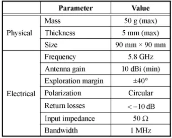
All previous requirements have led to the antenna specifications summarized in Table 1. The most-demanding requirements were the antenna's gain to achieve the desired
Table 1. The specifications of the antenna.
Physical
Electrical
Parameter
Mass
Thickness
Size Frequency
Antenna gain
Exploration margin
Polarization
Return losses
Input impedance Bandwidth
Value
50 g (max)
5 mm (max)
90 mm x 90 mm
5.8 GHz
10 dBi (min)
±40°
Circular
<-10dB
50 Q 1MHz
inter-satellite range, the antenna's thickness, and the return losses.
The exploration margin provides information about the maximum scan angle of the antenna's beam with respect to the broadside direction. The antenna gain requirement was derived from link-budget figures, with a receiver sensitivity of -100 dBm, and a transmitted power of -33 dBm, at 5.8 GHz, for a distance between satellites of 2 km. Due to the frequency of 5.8 GHz, issues such as losses and manufacturing errors had to be taken into account during the design phase.
3. Antenna Array Concept
Once the antenna specifications were clear, the next step was the definition of the antenna concept. Due to the particular limitations of the CubeSat platform, the students faced a chal-lenging engineering problem, where ingenious solutions were demanded.
The most obvious solution for an inter-satellite link antenna would be the use of omnidirectional antennas. How-ever, this approach has two main disadvantages: the maximum distance between satellites is significantly reduced, and the received RF signal does not provide any information about the relative position of the other spacecraft.
From the above specifications, it was clear that in order to satisfy the exploration margin requirement, an antenna with electronic beam-steering was required. We decided to opt for a planar phased antenna array with a modular design, where the available space for each element array was limited to 30 mm x 30 mm. From the mechanical requirements, the use of patch antennas as array elements was the most appropriate option at 5.8 GHz.
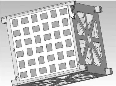
phase rotation in order to achieve the circular polarization. The maximum number of antenna elements in the planar array that fit in a CubeSat side was thus nine, under a 3 x 3 scheme. The antenna attached to the CubeSat platform is depicted in Figure 2.
As shown in Figure 3, different array configurations were feasible under the proposed approach, allowing the antenna array to be adapted to the available surface. Linear, rectangular, and square arrays could be implemented. The proposed antenna was a modular and scalable array of identical subarrays.
In order to steer the beam of the array, another layer with a phase shifter per subarray had to be included. A digital phase shifter was selected. In the satellite, the phase shifter was
con-Figure 2. The antenna array attached to the CubeSat plat-form.
3 cm
K
K
»
"I
K
K
K
»
a;
(a) 3x3 square array
K
K
K
(b) 3><2 rectangular array
Wr
-HH-• -HH-•
•
•
B
(c) 3 element linear array (d) 2x2 square array
Figure 3. Antenna array configurations in a square of 9 cm x 9 c m .
trolled by the onboard computer (OBC). The attitude and orbit control subsystem (AOCS) informs the onboard computer of the current attitude of the satellite. The communication sub-system process and sends to the onboard computer the infor-mation received from other satellites. The onboard computer is responsible for the calculation and distribution of the phase-shifter configuration to change the beam-steering direction. The update rate of the phase shifters' status depended on the "own attitude" of the satellite and the variation of the relative positions between CubeSats. After Monte Carlo simulations in
MATLAB, it was concluded that three bits to control the phase
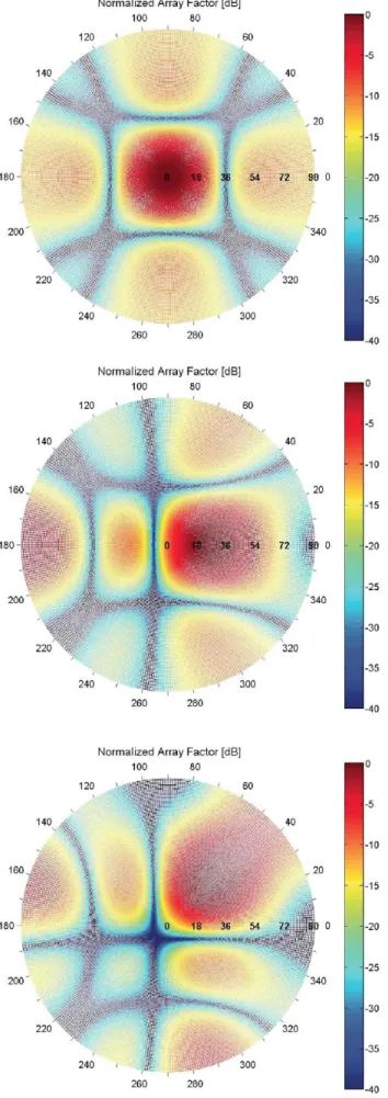
shifter, equivalent to a phase step of 45°, were required to have a pointing loss under 1 dB. Figure 4 shows the normalized array factor for three different beam-steering positions, using phase shifters of three bits. Using this approach, the onboard computer could perform beam scanning in order to search for a satellite of the cluster, or tracking once the satellite's position was acquired.
4. Antenna Design
The design phase of the antenna was divided into two tasks: the design of the array element, and the design of the phase shifter. These two tasks could be independently carried out, once the interface between the antenna and phase shifter was clearly defined.
The detailed design of the phase shifter is out of the scope of this paper. We will just mention that due to the high price of commercial phase shifters, we decided to design a three-bit phase shifter based on a switched-line technique [14]. The phase shifter was built over a substrate layer below the antenna, using a stripline structure with a duroid RT6010 substrate
Or= 1 0 . 2 ) . RT/duroid 6010 is approved for spacecraft
applications, due to its low coefficient of thermal expansion and outstanding resistance to out-gassing. The most challenging issues while designing the phase lines were the requirement to fit the whole phase shifter in an area of 30 mm x 30 mm, and the combination of RF and control paths in a single double-layer board. The phase shifter was formed by four RF switches, two SPDT (one control bit each) and two DPDT (four control bits each) (the RF switches were SPDT HCM849LP4CE and DPDT HMC393MS8G/393MS8GE, from Hittite.). The ten control signals could be generated either with a parallel interface of three control signals coming from the onboard computer and three logical inverters, or using a serial data interface, such as I2C or SPI.
We will next focus on the design of the array element.
Normalized Array Factor [dB]
100 80
2É 54 72 98 0
260 280
Normalized Array Factor [dB] 100 80
0 «¡í';'¡ W
260 280
Normalized Array Factor [dB]
100 80
260 280
1
1
Figure 4. The normalized array factors with a three-bit phase shifter: (a, top) broadside (0 = 0°, cp = 0°), (b, middle)
0 = 25°,cp = 0° , (c, bottom) 0 = 45°,^ = 45°.
enough to generate circular polarization, with four patches, the range of scan angles of the array beam at which the polarization maintained circularity was larger.
In order to achieve circular polarization, we selected a sequential phase-rotation method with a feed network to arrange 0°, 90°, 180°, and 270° phases, with a uniform power distribution to the patches [15]. This approach had several advantages over methods based on the use of single truncated patches. First, the use of rectangular patches allowed a signifi-cant reduction in the mutual coupling from that of a conven-tional array, as adjacent patches were orthogonally oriented. Second, both right- and left-hand circular polarization could be achieved by inverting the phase rotation, so that a transmitting/ receiving scheme using orthogonal polarizations at the same frequency could be achieved.
Regarding the substrates, we selected an FR4 substrate
with sr = 4.9 as a compromise among the maximum feasible
scan angle, the bandwidth, and the patch size. The slots, feed line, and ground plane were to be printed over a
high-permit-tivity duroid RT6010 ceramic-PTFE substrate (sr=l0.2
tan¿ = 0.0023).
The subarray was a multilayer structure. The top layer was formed by the four rectangular aperture-coupled patches with sequential rotation, printed over FR4. The patches were fed by a slot, since this technique did not require a direct connection between the feed network and the antenna [16]. The slots were placed in an intermediate RT6010 substrate layer in the ground plane between the patches (top) and the RT6010 feed network layer (bottom).
In the global design of the complete subarray, the number of variables and parameters to optimize was pretty large. The design procedure followed a "divide and conquer" approach. We divided the whole design problem into smaller problems that were separately solved. In a final step, all the designs were put together. The design steps were: (1) design of a single aperture-coupled patch; (2) design of the feed line to maximize coupling; (3) design of the feed network for uniform power distribution and sequential phase rotation; (4) integration and optimization of the multilayer design.
The subarray design started with the design of the single patch. A rectangular patch design was selected, in order to reduce mutual coupling between adjacent patches. The simu-lated 5*21 between adjacent orthogonally oriented patches was
-19 dB at 5.8 GHz, thus reducing the mutual coupling thanks to the use of rectangular patches.
the electric dipole [16]. A rectangular slot aligned with the patch and displaced half the resonant dimension of the patch was thus selected to maximize the magnetic-dipole coupling. The slot was placed with an offset relative to the patch's center to maximize coupling. The transmission line was enlarged with a stub of 0.25/1 to produce a maximum in the field under the slot due to the standing wave produced at the end of the line (open circuit). However, the line seemed to be electrically larger than its physical dimensions due to fringing effects, so that the final length ofthe stub was 0.22/1 [17].
After optimization to maximize the coupling, the follow-ing design values for the subarray were obtained:
Patch length: 10.4 mm
Patch width: 8 mm
Patch separation: 15 mm (0.64/1)
Length ofthe stub: 3.6 mm
Slot length: 6 mm
Slot width: 4 mm
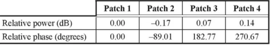
Two designs for the feed network were studied. The first one used a buried microstrip line under the aperture-coupled subarray. Feed lines started from the geometrical center of the subarray, had relative lengths that led to 90° degree phase shifts, and ended in the proper position under the coupling slots. The feed network had to fit in a 30 mm x 30 mm square, so that lines were formed by a combination of straight and bent lines [18]. After optimization ofthe bent lines and quarter-wave impedance transformers, the simulated amplitude and phase distributions ofthe feed network in Table 2 were obtained. The theoretical axial ratio achieved with the isolated feed network was 0.0971 dB in the broadside direction, leading to a perfect circular polarization.
As shown in Figure 5, The return losses were below -25 dB and the subarray gain was 5.1 dB, so that the complete array would satisfy the return-loss and gain requirements. The simulation of the subarray led to an axial ratio of 2.6 dB in broadside, and a scanning capability of +25° relative to
broad-side, for an axial ratio under 3 dB.
Although the performance was not optimal in terms of polarization purity, we decided to build a prototype based on the first design, for the students to get familiar with manufac-turing processes. The RF interface was an SMA connector that
was put in the lateral ofthe antenna, as it was not possible to use a transition from coaxial to microstrip from the center of the bottom layer (the ground plane was shared with the patch). As can be seen in Figure 6, the inner conductor distorted the antenna's structure, introducing some air near the conductor, thus drastically changing the performance ofthe antenna due to amplitude and phase imbalances. The measured return loss after adjustment was -14 dB (Figure 7).
S- Para meter Magnitude in dB
Figure 5a. The simulated return losses ofthe first subarray design.
Figure 5b. The simulated radiation pattern of the first subarray design.
Figure 6. The first prototype: a detail of the lateral SMA connector.
Table 2. The power and amplitude distributions after optimization of the feed network in the buried microstrip line.
Relative power (dB)
Relative phase (degrees)
Patch 1
0.00 0.00
Patch 2
-0.17 -89.01
Patch 3
0.07 182.77
Patch 4
File View Channel Sweep Cajibration Trace Scale Market System Window Help
Stimulus Start 3.00OHIO0OHIO GHz [ j j Start | Stop Center Span IS11
5.000dE7 |0.00dB LogM|
25.00
20.00
15.00
10.00
5.00
ooo ¥
5.00
•10.00
•15.00
•20.00
•25.00 Chi:
^ _ . d d n d o 7 r o , illos
Start 3.00000 GHz Status C H I : S11 ] CA1-Port
A
\I \
Delay
X
Stop 7.00000 GHz LCL
Figure 7. The measured return losses of the first prototype.
As a solution to solve the problem found with the previ-ous feeding technique of the antenna, we tried a different, sec-ond feeding network design to improve the coupling from the connector to the patches, and to minimize errors in the distri-bution of power and phase in the feed network. We also com-promised in making a more-realistic electromagnetic simula-tion of the subarray, including the CAD of the SMA connector.
The new design was a stripline feed network, in order to have two ground planes [19]. With this technique, the antenna could be fed from the central part of the subarray, using a con-ventional SMA connector. A problem arose when we simulated the single patch to see which minor changes should be done in order to address the new geometry. The result was a very low coupling between the line and the patch, due to several facts:
In the first design, the end of the microstrip line made an open circuit in the structure, forcing the wave to reflect, and produce a standing wave that enhanced the coupling through the slot. However, in this new design, the wave did not find an open circuit at the end of the line, since it could still propagate in a different mode (the parallel-plate mode) between both ground planes.
the slot, the geometry was the same geometry as a transition from stripline to microstrip line. The field thus concentrated more between the line and the upper ground plane (trying to accommodate the new microstrip-line geometry) and got further from the slot.
Here, we will focus on the second problem, which was the problem that most reduced the coupling. To prevent the field from skipping the slot, we wanted to reduce the slot's length in order to make the wave not see a microstrip-line geometry; however, as we reduced the slot length, the coupling was obviously reduced. For this purpose, we divided the slot into two consecutive slots. However, it is more illustrative if we did not view it as two slots, but as one slot with a metallic line in the middle. What this metallic line did was to attract the electric field, and prevent it from concentrating on the opposite ground plane. Nevertheless, the coupling factor did not rise at all. The problem was that the slot was placed to use a magnetic-dipole coupling, but we were now using a coupling mechanism through the electric field. We thus had to move the slot back to the center of the patch (where the coupling through the electric dipole was maximized), although it would always be lower than the results obtained for the magnetic dipole.
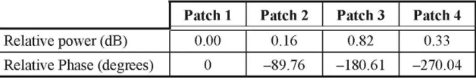
The power and phase distributions after the feed-network design are shown in Table 3. The axial ratio achieved with the feed network was 2.04 dB in the broadside direction, due to the power imbalance in the third branch.
The second subarray design resulted in the following parameters:
Patch length: 10.5 mm
Patch width: 8 mm
Patch separation: 15 mm (0.64/1)
Length of the stub: 3.2 mm
Slot length: 3 mm
Slot width: 4.3 mm
In the first design, when the wave arrived at the slot, it had no more options (apart from being reflected) other than propagating through the slot. In contrast, in the second design, when the wave arrived at
The multiple-layer structure of the final subarray is shown in Figure 8. The total thickness of the antenna was 2.87 mm, plus the negligible thickness of the ground-plane layer and the patch antennas' conductor (17 |am each).
Table 3. The power and amplitude distributions after optimization of the feed network in stripline.
Relative power (dB)
Relative Phase (degrees)
Patch 1
0.00
0
Patch 2
0.16
-89.76
Patch 3
0.82
-180.61
Patch 4
0.33
S R T 6 0 1 0 ( 2 X O . - S 3 5 T T ¡
Ü
Ground p ¿ r e with slot < Feed Network < Ground plane
Coaxial inner conductor (rj)=1.3 mm
- Coaxial outer conductor [fy=4.1 n
Figure 8. The side view of the 2 x 2 subarray (multilayer structure).
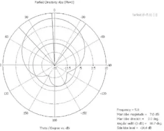
Figure 9 shows the simulated return losses of the second and final 2 x 2 subarray. Lossy substrates were considered in the simulation. The -10 dB bandwidth of the subarray was 138 MHz, or a 2.4% fractional bandwidth. The radiation pattern of the subarray presented an antenna gain of 6.9 dBi with a beamwidth of 80.7°, as shown in Figure 10. The subarray pattern presented a beam-center deviation of 3°, equivalent to a negligible miss-pointing loss of 0.017 dB.
s-P„m.t.,r, agnitiide in dB;
Figure 9. The simulated return losses of the final 2 x 2 subarray.
Type Appro Mo n i t Compo Dutpu hrequ Rad. T o t . D i r .
x i m a t i o n or nent t ency e f f i c . e f f i c .
farfield enabled (kR » 1) farfield (f=5.8) [1]
Figure 10a. The simulated three-dimensional pattern of the final subarray.
-arfield Directivity Abs (Ph=o;
Farfield (f=5.8) [1]
-requency = 5.S ^aln lobe magnitude = 7.0 c
Side lobe level = -14.4 dE
Figure 10b. A cut through (p = 0° of the simulated three-dimensional pattern of the final subarray.
5. Final Prototype and Measurements
5.1 Prototype
As commented above, the first subarray prototype did not provide the expected results for return losses and antenna pat-tern. Figure 6 shows the lateral position of the RF connector. The inner conductor had to be inserted between two layers to assure proper contact with the feed line, leading to a deforma-tion in the antenna prototype, due to the separadeforma-tion between layers.
The three layers of the second prototype, based on a strip-line feed network, were separately printed and tooled in the circuit laboratory. Apart from the patches, slots, and feed lines, four holes in the corners were included in the Gerber files of the layers, to place screws in order to pack the three layers together, avoiding empty spaces. In Figure 11, the individual layers before stacking are shown, while Figure 12 shows a lateral view of the subarray. The size of the subarray was 40 mm x 30 mm, to include some extra space for allocating plastic screws in the corners. The weight of the complete subarray prototype, including the SMA connector (4 g) and screws, was 14 g.
5.2 Measurements
We started with the measurement of return losses. After proper instruction, students had the opportunity to calibrate the VNA (vector network analyzer) and measure return losses, themselves. Due to the small size of the antenna and stiffness of the vector network analyzer cables, we could not firmly fix the subarray, and had to make these measurements with the antenna "on the air." We noticed a large variation in the resonances and return-loss level when we changed the position of the antenna and cables during the setup of the test. Also, a large variation in the Sn with the pressure on the antenna connector while moving the cable was confirmed.
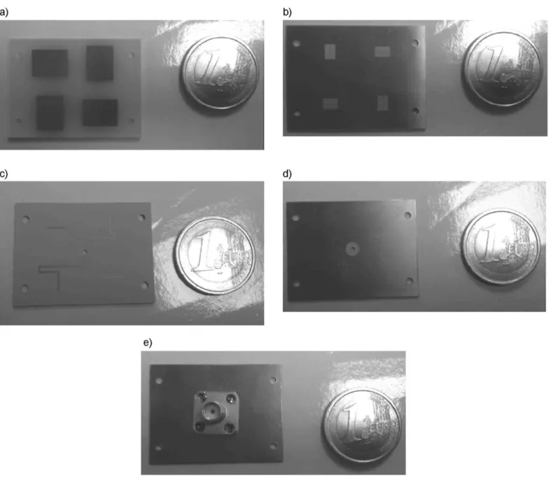
Figure 11. The individual layers of the second subarray prototype: (a) top layer: patches; (b) mid-layer: slots; (c) bottom layer (top): feed and phasing network; (d) bottom layer (bottom): SMA interface; (e) bottom layer (bottom): SMA connector.
File View Channel Sweep Cajibialion Trece Scale Marker S^slem Window Help
Marker: 1 el 3 Marker 1 | 5.8Ü0Q0Ü0Q0Ü GHz Q Marker 1 Marker 2 Marker 3 Off
IS11 5.000dE7 |0.00dB LogM|
1
25.00
20.00
15.00
10.00
5.00
5.00
-10.00
•15.00
•20.00
•25.00 Chi:
^ HA
~~'
\ ,
\ /
2:
3-N
5.7000 sqnnn¡ 30 GHz - 3456 ';
5 7flfi HR
A
H
:
Start 5.00000 GHz Stop 6.00000 GHzStatus C H I : S11 ] C 1-Port LCL
Figure 13. The measured return losses of the final proto-type.
5.8 GHz, even outperforming the simulation predictions. The measured -10 dB return-loss bandwidth was larger than 250 MHz, or 4.3% fractional bandwidth.
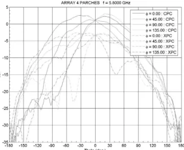
The next step was the measurement of the radiation pat-tern in anechoic chamber (Figure 14). Students had the opportunity to prepare the setup of the antenna in the positioner, and to understood the importance of antenna alignment and probe calibration. These tests were carried out in the spherical near-field chamber of the Laboratorio de Ensayos y Homologación de Antenas of Universidad Politécnica de Madrid (LEHA-UPM). The measured co-polar and cross-polar radiation patterns of the subarray for different cp cuts are depicted in Figure 15. In the principal planes (cp = Q° and
cp = 90°), the pattern showed a slight miss-pointing with
respect to the broadside direction, with a beamwidth of 80°. The measured gain of the subarray was 2.5 dBi, lower than expected, and degrading the resulting axial ratio in the vicinity of broadside.
Figure 14. The subarray on the anechoic-chamber posi-tioner.
6. Discussion and Lessons Learned
When measurements of the final prototype were avail-able, we discussed trying to find the answer to the results for the radiation pattern and axial ratio. Several potential error sources were identified. In order to explain the degradation in the axial ratio, we looked at the dimensions of the prototype. In the simulation, the size of the subarray was fixed to a square of 30 mm on a side, whereas the prototype size was 40 mm x 30 mm in order to leave some space for the screws. We analyzed the axial ratio for the two subarray sizes (square and rectangular) via simulation, and found out that the lack of symmetry of the structure had significantly degraded the axial ratio, producing an elliptical polarization. A prototype of 40 mm x 40 mm would thus have been more appropriate. This effect should be taken into account in the design of the whole array, because elements (subarrays) located at the edges and in the corners of the array would have an asymmetry in their ground planes.
A R R A Y 4 P A R C H E S f = 5.8000 G H z
• = 0.00 : C P C t = 45.00 : C P C t = 90.00 : C P C -• = 135.00: C P C t = 0.00 : X P C t = 45.00 : X P C -t = 90.00 : X P C • = 135.00: X P C
Figure 15. The measured radiation patterns.
The second source of degradation was the metallic screws. In the simulation during the design phase, we did not include any item apart from the antenna layers, as we initially had decided to use plastic screws. Apart from the four screws in the corners of the subarray prototype, there were another four screws close to the patches. After including the metallic screws in the electromagnetic simulation, we confirmed that they had two effects on the antenna's performance: (1) the radiation of the individual patches was distorted in the presence of the metallic screws, and (2) the axial ratio was degraded.
In addition, we studied the impact of a thin air layer in the antenna, representing a bad packing of the layers, via electromagnetic simulation. The results showed a degradation in the return losses of the antenna, and a variation of the reso-nance frequency.
as any error or misalignment implies a significant distortion in the electrical performance at a frequency of 5.8 GHz. More-over, students realized that both the electrical and mechanical performance are equally important when designing antennas for space systems.
Finally, it is important to remark that a preliminary study of the impact of the launcher's vibration on the antenna was carried out. The antenna was modeled as a sandwich structure, with layers having properties that were identical to the antenna's substrates. The results showed that displacements of the layer along the antenna's plane were minimal (a tenth of a micron) after applying launch forces in the simulator. Deformations in the direction normal to the antenna showed values below 1.5 urn. We therefore concluded that the proposed antenna structure was compact and robust against the conditions of the launch environment.
7. Educational Outreach
The idea of the project started in collaboration with a group of students that tried to find a novel mission, payload, or subsystem concept to be integrated onboard a nanosatellite, preferably a CubeSat. The initial group was formed by 15 students of the Master in Telecommunication Engineering in ETSIT-UPM, with different backgrounds ranging from second to fifth year. The participation was also open to PhD students, researchers, and lecturers interested in space technology.
After several sessions, coordinated and supervised by a faculty professor and celebrated as part of elective activities in the area of nanosatellites, ideas related to space networking protocols, communication techniques, and inter-satellite com-munications come out. We finally decided that the most origi-nal idea with the best future projection was the design of an antenna array for inter-CubeSat communications. With the available resources and equipment, we knew we would have the opportunity not only to face the design of the antenna, but also to build and measure its performance. Other brilliant ideas considering new mission concepts for nanosatellite utili-zation were successfully submitted by students to an interna-tional competition entitled Mission Idea Contest (http://www. spacemic.net).
The first set of antenna specifications was proposed and derived by the group of students under the supervision of a faculty staff member. These initial specifications were then refined by the student who took the compromise to build the antenna as part of his masters thesis.
Feasibility study and specifications
First antenna prototype Antenna design and optimization * CAD and manufacturing • Measurements
Second antenna prototype • Antenna design and
optimization • CAD and manufacturing • Measurements Phase shifter • Design * CAD and manufacturing
M l : Ant una concept a
-•_
M3: Second antenna prototype
M4: Final report
- •
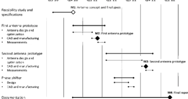
Figure 16. The project schedule, tasks, and milestones.
out, and the PCB was manufactured. However, a prototype of the phase shifter was not constructed, because the available instrumentation for soldering the RF switches was not fine enough.
It is also important to say that the student that performed the work dedicated part time to the work, 20 hours of effort per week.
In order to ensure the continuity of the project once stu-dents finish their studies, proper documentation with adequate configuration control was required. Moreover, the archival of the CAD and simulation files with all the preliminary designs required an efficient and flexible file-management system.
8. Conclusions
In this paper, the experiences from an educational project for the specification, design, construction, and measurement of an antenna array for inter-satellite communications, tailored to CubeSat and nanosatellite missions, have been presented. With a principal focus on the hands-on training of students, the proposed antenna satisfied the initial requirements. It can be considered as a first-concept demonstrator in the area of inter-satellite links between CubeSats.
Another important aspect of the educational scope of the project was its multidisciplinary nature. As shown through the paper, not only electromagnetic and antenna knowledge were required to design the antenna array, but also requirements coming from the mission and other spacecraft subsystems had to be understood and taken into account. This all emphasized the system engineering aspects of the project.
The duration of the whole project was 21 months, includ-ing holiday periods. The calendar with tasks and milestones is depicted in Figure 16. Some delays were experienced, due to the availability of circuit laboratory and the lack of anechoic-chamber slots for the antenna measurement. Throughout the design of the second antenna prototype, some instability problems in the simulation of the antenna structure had to be solved. In parallel, the design of the phase shifter was carried
The educational project was organized as a real engineer-ing design challenge, and covered most of the lifecycle phases of an engineering project:
Design: familiarization with software packages such as MATLAB and spreadsheets for preliminary sizing of the antenna, and with CAD software such as CST
Microwave Studio for full electromagnetic analysis
Component selection: contact with manufacturers and distributors, and understanding the datasheets of materials and other components that matched the specifications
Prototyping: dealing with hands-on issues that appear when fabricating an antenna, such as sol-dering, the stacking and alignment of layers, manual adjustments, etc.
Measurement: getting familiar with laboratory equipment, e.g., vector network analyzers and anechoic-chamber measurement techniques
Documentation: writing of technical reports
Dissemination: the preliminary results of the pro-ject were presented at the Spanish National URSI
symposium
It is particularly important to mention that the whole pro-ject was successfully carried out with a very limited monetary budget. If manufacturers confirmed the availability of samples, the cost of materials for the antenna array was negligible. As well, the use of facilities in the university for this education project reduced to zero. This approach is of course not feasible for the development of a whole CubeSat, where funding from sponsors is required and must be available at the beginning of the project. Regarding substrates and components, manufac-turers provided samples for the two prototypes. Tooling and measurements were done in the facilities available in the Radiation Group laboratory, where all the required equipment is open to the use of students participating in training programs under faculty staff supervision. Therefore, we have shown that it is possible to implement hands-on activities with students similar to real engineering projects, with a limited budget and promising results.
The next steps of the project are the optimization of the antenna element to improve the axial ratio, and the construc-tion of the whole array, including the phase-shifter module, to measure and validate the beam-steering capabilities of the antenna array. These tasks are part of the long-term education project denoted as TelCUBE (http:// telcube.blogspot.com), and will be continued and carried out by students.
9. Acknowledgments
The authors gratefully acknowledge the Spanish Ministry of Science of Innovation for the partial funding of this work under the SICÓMORO project (TEC2011-28789-C02-01). The authors would also like to thank Universidad Politécnica de
Madrid and ETSI de Telecomunicación (ETSIT-UPM) for the support and the partial funding of this training project under Innovative Education Programmes (TelCUBE Project). The authors also thank Rogers Corp and Altaix S.A. for providing samples of substrates and RF switches, and CST for providing educational software licenses and technical support for CST
Microwave Studio.
10. References
1. H. Heidt, J. Puig-Suari, A. S. Moore, S. Nakasuka, and R. J. Twiggs, "CubeSat: A New Generation of Picosatellite," Pro-ceedings of the 15th Annual AIAA/USU Conference on Small Satellites, Logan, UT, August 2001.
2. CubeSat Design Specification (CDS), Rev. 12, The CubeSat Program, CALPOLY SLO; available at http:// www.CubeSat. org.
3. S. Greenland and C. Clark, "CubeSat Platforms as an On-Orbit Technology Validation and Verification Vehicle," Pro-ceedings of the 2010 European Small Satellite Services Sym-posium, Madeira, May 31 - June 4, 2010.
4. J. Muylaert, C. Asma, W. J. Ubbels, J. Rotteveel, V Danilkin, and S. Makhankov. "QB50: An International Network of 50 CubeSats in LEO for Lower Thermosphere and Re-Entry Research," Proceedings of the 23rd Annual Conference on Small Satellites, CubeSats Developer's Workshop, Utah State University, USA, August 8-9, 2009.
5. A. J. Ridley et al., "The Armada Mission: Determining the Dynamic and Spatial Response of the Thermosphere/Ionosphere System to Energy Inputs on Global Regional Scales," AU Fall Meetings Abstracts, San Francisco, Dec. 2010, pp. A7+.
6. C. Swenson et al., "The International Space Station as a Launch Platform for CubeSats to Study Space Weather," Pro-ceedings of the 3rd Nanosatellite Symposium, Kitakyushu, Japan, December 12-14, 2011.
7. F Aguado, "HUMSAT Project," Proceedings of the 7th Annual CubeSat Developers' Workshop, San Luis Obispo, CA, April 21-23, 2010.
8. O. N Challa and J. McNair, "Distributed Computing on CubeSat Clusters using MapReduce," Proceedings of the 1st Interplanetary CubeSat Workshop, Cambridge, MA, May 29-30, 2012.
9. K. T Alfriend, S. Rao Vadali, P. Gurfil, Jonathan P. How, and Louis S. Berger, Spacecraft Formation Flying: Dynamics,
Control, and Navigation, New York, Elsevier, 2010.
Nasimuddin (ed.), Microstrip Antennas, Rijeka, Croatia, InTech, 2011; available at http://www.intechopen.com/books/ microstrip-antennas/electrically-small-microstrip-antennas-targeting-miniaturized-satellites-the-CubeSat-paradigm.
11. N. G. Orr, J. K. Eyer, B. P. Larouche, and R. E. Zee, "Pre-cision Formation Flying: The CanX-4 and CanX-5 Dual Nanosatellite Mission," Proceedings of the 21st AIAA/USU Conference on Small Satellites, Salt Lake City, UT, August 2007.
12. A. Chandrasekaran, J. E. Gutshall, and C. M. Swenson, "The Design of the Communication and Telemetry System Used by the Ionospheric Observation Nanosatellite Formation Mission," Proceedings of the AIAA/USU Conference on Small Satellites, August 2001.
13. M. Marszalek, O. Kurz, M. Drentschew, M. Schmidt, and K. Schilling, "Intersatellite Links and Relative Navigation: Pre-conditions for Formation Flights with Pico- and Nanosatellites," Proceedings of the 18th IFAC World Congress, Milano (Italy) August 28-September 2, 2011, pp. 3027-3032.
14. R. J. Mailloux, Phased Array Antenna Handbook, Second
Edition, Norwood, MA, ArtechHouse, 2005.
15. J. Huang, "A Technique for an Array to Generate Circular Polarization with Linearly Polarized Elements," IEEE
Trans-actions on Antennas and Propagation, AP-34, 9, September
1986, pp. 1113-1124.
16. D. M. Pozar, "Microstrip Antenna Aperture-Coupled to a Microstripline," Electronics Letters, 21, 2, January 1985, pp. 49-50.
17. P. L. SullivanandD. H. Schaubert, "Analysis of anAperture Coupled Microstrip Antenna," IEEE Transactions on Antennas
and Propagation, AP-34, 8, August 1986, pp. 977-984.
18. D. M. Pozar, Microwave Engineering, Third Edition, New York, Wiley, 2007.
19. A. Bhattacharyya, O. Fordham, and Y. Li, "Analysis of Stripline-Fed Slot-Coupled Patch Antennas with Vias for Par-allel-Plate Mode Suppression," IEEE Transactions on