Degradation mechanism analysis in temperature stress tests on III-V
ultra-high concentrator solar cells using a 3D distributed model
P. Espinet
3'*, C. Algora
3, J.R. González
3, N. Nunez
a'
b, M. Vázquez
a'
b^Instituto de Energia Solar - Universidad Politécnica de Madrid, E.T.S.I Telecomunicación, Avda. Complutense 30, 28040 Madrid, Spain bEUIT de Telecomunicación, Campus Sur-UPM, Km. 7 Carretera de Valencia, 28031, Madrid, Spain
A B S T R A C T
A temperature stress test was carried out on GaAs single-junction solar cells to analyze the degradation suffered when working at ultra-high concentrations. The acceleration of the degradation was realized at two different temperatures: 130 °C and 150 °C. In both cases, the degradation trend was the same, and only gradual failures were observed. A fit of the dark l-V curve at 25 °C with a 3D distributed model before and after the test was done. The fit with the 3D distributed model revealed degradation at the perimeter because the recombination current in the depletion region of the perimeter increased by about fourfold after the temperature stress test. Therefore, this test did not cause any morphological change in the devices, and although the devices were isolated with silicone, the perimeter region was revealed as the most fragile component of the solar cell. Consequently, the current flowing beneath the busbar favors the progression of defects in the device in the perimeter region.
1. Introduction
High-concentration photovoltaic (CPV) systems seem to be one of the most promising ways to generate electricity at competitive prices for terrestrial applications [1]. In the past decade, the effi-ciency of multi-junction solar cells has increased considerably [2-5]. Nevertheless, the CPV community is aware that, together with the efficiency increase, high reliability is essential for reducing the cost of solar electricity by extending the system's lifetime [6]. Silicon modules are reliable systems that have performed well in the field with less than 1% degradation/year for more than 20 years [7]. However, the knowledge of the reliability of III-V solar cells is still scarce [8-12]. This work identifies the failure mechanism in an accelerated temperature stress test carried out on GaAs solar cells in order to improve the quality of these devices. The aim of this work was to analyze the failure mechanism of this kind of solar cell using a 3D distributed model based on elemental circuit units [13]. In this article, we show the potential of the 3D distributed model in the evaluation of degradation in III-V solar cells.
2. Experimental
2.1. Assembly description
The assembly of the solar cells used in this test presented the following characteristics: (a) encapsulation on direct-bonded
* Corresponding author.
E-mail address: [email protected] (P. Espinet).
copper (DBC) substrates improved the thermal dissipation, (b) encapsulated cells were attached to an aluminum box with a ther-mal-conductive adhesive, and (c) cells were covered with silicone to simulate a real situation of the solar cell inside the secondary optics in a concentrator.
2.2. Test methodology
The acceleration of the degradation was performed by means of temperature stressing. Two sets of 18 solar cells were placed inside climatic chambers at different temperatures of 130 and 150 °C. Be-cause the solar cells inside the climatic chambers were in darkness, the current mainly flowed vertically beneath the busbar [13]. The area of the busbar was 0.64 mm2. Therefore, assuming that the
short circuit density current of this kind of solar cell is 25 mA/ cm2 at 1 x, working conditions at 700 x were simulated by injecting
112 mA into each solar cell. A detailed description of the acceler-ated test can be found elsewhere [14].
3. 3D distributed model
3.1. Model description
and perimeter (Figs. 1 and 2). The complete solar cell is modeled by the electrical circuit obtained by interconnecting every unit cell with its neighbor. The resulting equivalent circuit formed by thou-sands of elements is resolved using the SPICE circuit simulator. The fitness of this model for the analysis of the degradation mechanism is derived from the treatment of the loss effects in a distributed manner.
For the ohmic losses, a set of resistors modeling the different series resistance components was used (front grid, semiconductor layers; front and back contacts, substrate). Regarding the nation phenomena, three diodes were used to model the recombi-nation in the neutral regions (ideality factor ni = l), in the depletion regions (ideality factor n2 = 2) and at the perimeter
(ide-ality factor n2PER = 2). It is important to note that a reasonable fit
between experimental measurements and simulations can be achieved using other ideality factors. However, the parameters 7oi,7o2 and JO2PER obtained from such a strategy are mathematical
parameters that lack a direct physical meaning. The extension of this model to multi-junction solar cells including tunnel junction description has been already done [15].
3.2. Explanation for the dark I-V curve in GaAs solar cells
Simulations of a typical GaAs solar cell varying the values of more relevant parameters in the dark I-V curve were carried out to obtain a better understanding of the results presented in Section 4.
The effect of series resistances is observed at high voltages. In the I-V curve, the lateral resistances such as the emitter sheet
10u
10-1
-i—i
c 0)
| l o3
o
io-410
I
rv
=| ^
1-10"4ohms/cm21-10"3ohms/cm
10-10'2ohms/cm2
0.8 0.9 1.0 1.1
Voltage, V(V)
1.2 1.3
Fig. 3. Variations of the vertical resistance (rv), which take into account the resistance at the base, in the BSF layer and in the back contact.
resistance (rE), the base sheet resistance (rB) and the metal sheet
resistance (rM) have a negligible impact on the curve because the
current mainly flows vertically beneath the busbar [13]. On the other hand, both the vertical resistance (rv) and the front grid
spe-cific contact resistance (rFC) show a large influence under dark
con-ditions (see Fig. 3). However, the effect of the shunt resistances at the bulk (rp) or at the perimeter (rpPER) is observed at low voltages
(see Fig. 4). Previous studies of the degradation in GaAs solar cells without perimeter isolation revealed changes in the shunt resis-tance at the perimeter [8].
Perimeter Dark area Illuminated
region
a r e aFig. 1. 3D network model for a single-junction solar cell.
/ rM ,/'
/ / /
• V F C
/
7
r
EJo2PERy |rp P E I
/
/ r
B* r
/ i
?
/ / rM /
7tr
/
"7
W V ^ >
rE Jo2
Joi^fj
• ^ A A r - i
¿?"
•*_ i "/ T
°—vw^
A
W r
-Jo2
D
/ r
B"•. r
/ / S 'v / ]
1
/
/
0.00 0.25 0.50 0.75 1.00
Voltage, V(V)
1.25
Fig. 4. Variations of the shunt resistance in the perimeter region (rPPER).
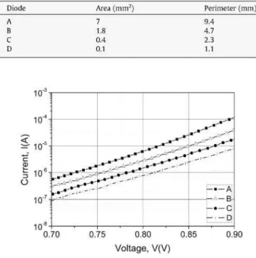
a study of the perimeter recombination in our growth material and our technology was essential. Circular diodes of GaAs with four dif-ferent sizes (Table 1) were processed to study the recombination mechanism at low voltages.
In Figs. 7-9, the dark I-V curve, the J- V curve and the lineal den-sity current at the perimeter versus voltage are depicted, respec-tively, for representative examples of a large number of diodes for each size. From these figures it can be inferred that, as expected, at low voltages the current correlates with the area in agreement with Refs. [16-19]. Therefore, I02 is smaller than /02PER. and its
influence is negligible.
4. Results
In all cases tested, only gradual failures were observed, and the degradation trend was the same for the two groups of solar cells tested at different temperatures. Therefore, the same failure
mech-10°
io-1
10"3
10"4
10"
0)
O
;.—v
V
:
!
j T
= 1 10"18A/cm2
= 2-10"19A/cm2
= 5-10'19A/< ;m2
0.8 0.9 1.0 1.1 1.2 1.3
V o l t a g e , V ( V )
Fig. 5. Variations of the recombination current density in the neutral regions (]0
-0.9 1.0 1.1 1.2
Voltage, V(V)
1.3
Fig. 6. Variations of the recombination current density at the perimeter (J0: The p a r a m e t e r 7oi takes into account t h e recombination at t h e neutral regions. The main influence of this p a r a m e t e r occurs at high voltages (Figs. 5 and 6).
The parameters J02PER a n d J02 b o t h have an effect at low volt-ages; however, several studies in GaAs [ 1 6 - 1 9 ] s h o w t h a t t h e a m p l i t u d e of t h e recombination current w i t h ideality factor n = 2 does not correlate w i t h t h e area; instead, it correlates w i t h t h e perimeter. A previous study of degradation in GaAs solar cells re-vealed changes in t h e I-V curve at low voltages [8]; consequently,
Table 1
Dimensions of the diodes of GaAs used in the study of the recombination current at low voltages.
Diode
A B C D
Area (mm2)
7 1.8 0.4 0.1
Perimeter (mm)
9.4 4.7 2.3 1.1
10 T
104
10"
E m6
IO"'
10"
y-r:--. - • — y i - - „ • —
^
Jr^^'
. . • • '
— A
- • - C - i - D
0.70 0.75 0.80 0.85
Voltage, V(V)
Fig. 7. Dark I-V curves of the GaAs diodes of different sizes.
10'
0.90
¡
10'2£
10'
ci
I 10 = i O
10"
i -'t^-te^-
¿-^A^L,-'~=3É
- • - A - A - B - • - C - i - D
0.70 0.75 0.80 0.85
Voltage, V(V)
0.90
£ o
3
3
|
03 Q . O IU 1- i n -í -1U :
l n- 5 . IU
io6^
:
irv'-F * "
_.•<
• - ' • j
^ j
s¿S*
— A
—a— B
- • - C
- - D
-,
Table 2
Parameters used in the fits of Fig. 9.
0.70 0.75 0.80 0.85
Voltage, V(V)
0.90
Fig. 9. Linear current density (J/P) versus voltage of the GaAs diodes of different
sizes.
anism was responsible for the degradation in all of the solar cells. To analyze the degradation mechanism, different fits with the 3D distributed model explained in Section 3 were carried out at 25 °C before and after the test. Fig. 10 is a representative case of the 18 solar cells studied at each temperature. An accurate descrip-tion of the GaAs solar cell before and after degradadescrip-tion was ob-tained with the 3D distributed model.
The parameters used in the fits of Fig. 10 are presented in Table 2.
Using Table 2, we can conclude that the solar cells degraded in the perimeter region because the recombination current density in the depletion region at the perimeter (/02PER) is the only parameter
that changed in the fits. After the accelerated test at 130 °C, J02PER
was almost fourfold higher than before the test. Even though the perimeter was passivated with silicone, it seems to be the most fragile part of the solar cell; the current flowing beneath the busbar favors the progression of defects in the device perimeter and thus causes an increase in the dark current. Hence, because the perim-eter is not passivated, the gradual degradation in GaAs solar cells might proceed as follows [20]: (1) non-radiative (n = 2) recombina-tion occurs at some defects at the perimeter, which causes a point defect reaction and fresh point defect generation and (2) the new defects also act as non-radiative recombination centers, and thus this process increases theJ02PER. Also, the silicone caused thermal
oxidative degradation after the test. Therefore, the oxidation of the organic groups and degradation of the main chain of the mol-ecule can have an effect on the unpassivated perimeter.
0.8 0.9 1.0 1.1
Voltage, V(V)
Experimental before degradation Simulation before degradation • Experimental after degradation — Simulation after degradation
f-1.2 1.3
Parameter
Joi (A/cm2) ;0 2 (A/cm2)
7O2PER (A/cm)
rFC (ÍJ cm2) rv ( n cm2) rp ( n cm2) rpPER ( n cm) rE ( n D) rB ( n D)
rM ( n D)
Before
1 x K T1 9 1 x l O "1 1 1.95 x 1(T12 2 x 1(T4 1 x K T4 1 x l O5 1 x l O5 200 600 0.2
After
1 x 10⁻¹ 9 1 x 1 0 - " 8 x 10~12 2 x 10~4 1 x 10⁻⁴ 1 x 10⁵ 1 x 10⁵ 200 600 0.2
Fig. 10. Measured dark I-V curve of the solar cell before (black circles) and after
(white triangles) the accelerated degradation test. Fit with the 3D distributed model before (dotted line) and after the test (solid line).
Note that a satisfactory fit could be achieved by varying the J02
parameter and fixing JO2PER or by modifying both parameters. Therefore, a previous understanding of the device is necessary to obtain a physically significant fit.
The increase in saturation current at the perimeter leads to a decrease in the fill factor and the open circuit voltage, resulting in a slight decrease of efficiency. However, it has to be mentioned that the relative decrease in power would be more prominent in applications with lower concentration.
Finally it must be pointed out that this test did not cause any morphological changes in the devices.
5. Conclusions
In this paper, the failure mechanism in temperature stress test-ing of GaAs solar cells accordtest-ing to a 3D distribution model was studied. Fits ofthe/-Vcurve at 25 °C with the 3D distributed model before and after degradation were done. An accurate description of the solar cell before and after degradation was obtained with the model. Furthermore, the model revealed that the degradation takes place in the perimeter region because the recombination current density at the perimeter increased by a factor of 4. Results of this study confirm that GaAs concentrator solar cells are resistant de-vices because neither catastrophic failures nor morphological changes occurred.
Acknowledgments
This work was supported by the Spanish Ministerio de Educa-ción y Ciencia with the CONSOLIDER-INGENIO 2010 program by means of the GENESIS FV Project (CSD2006-004). The Spanish Ministerio de Ciencia e Innovación has also contributed with the SIGMASOLES Project (PSS-440000-2009-30) and with the project with reference TEC2008-01226 as well as the Comunidad de Madrid under the NUMANCIA II programme (S2009/ENE1477).
References
[1] Yamaguchi M, Luque A. IEE Trans Electron Dev 1999;46:2139-44. [2] García I, Rey-Stolle I, Galiana B, Algora C. Appl Phys Lett 2009;94:053509. [3] Geisz JF, Friedman DJ, Ward JS, Duda A, Olavarria WJ, Moriarty TE, et al. Appl
Phys Lett 2008;93:123505.
[4] Guter W, Schone J, Philipps SP, Steiner M, Siefer G, Wekkeli A, et al. Appl Phys Lett 2009;94:223504.
[5] King RR, Law DC, Edmondson KM, Fetzer CM, Kinsey GS, Yoon H, et al. Appl Phys Lett 2007;90:183516.
[6] Kurtz JGS, Quintana M. Society of photographic instrumentation engineers (SPIE), San Diego, California (USA); 2009.
[7] Osterwald JACR, del Cueto JA, Korposki B, Trudell D, Moriarty T. In: 32nd IEEE photovoltaic specialist conference; 2006. p. 2085-8.
[8] Gonzalez JR, Vazquez M, Nunez N, Algora C, Rey-Stolle I, Galiana B. Microelectron Reliab 2009;49(]uly):673-80.
[9] Rey-Stolle I, Algora C. Prog Photovoltaics 2003;ll(]une):249-54.
[10] Schone GPJ, Hoheisel R, Siefer G, Guter W, Dimroth F, Bett AW. In: 23rd European photovoltaic conference and exhibition, Valencia (Spain); 2008. [11] Araki HUK, Kondo M, Takamoto T, Agui T, Kaneiwa M, Egami T, et al. In: 31rd
[12] van Riesen S, Bett AW. Prog Photovoltaics 2005;13(August):369-80. [16] Henry CH, Logan RA, Merritt FR. J Appl Phys 1978;49(6):3530-42. [13] Galiana B, Algora C, Rey-Stolle I. Prog Photovoltaics 2008;16:331-8. [17] Mazhari B, Morkoc H. J Appl Phys 1993;73(11):7509-14. [14] Núñez N, Vázquez M, González JR, Algora C, Espinet P. In: ESREF; 2010 [18] Belgachi A. Microelectron J 2005(36):115-24.
[15] Espinet P, Garcia I, Rey-Stolle I, Algora C, Baudrit M. In: Proceedings of the [19] DeMoulin PD, Tobin SP, Lundstrom MS, Carpenter MS, Melloch MR. IEEE international conference on concentrating photovoltaic CPV6, Freiburg Electron Dev Lett 1988;9:368-70.