NGCPV: A NEW GENERATION OF CONCENTRATOR PHOTOVOLTAIC CELLS, MODULES AND SYSTEMS (A FINAL REVIEW)
A.Datas1, A.B. Cristóbal1, G. Sala1, I. Antón1, J.C. Miñano1, P. Benitez1, C. Algora1, A.W. Bett2, D. Lackner², M. Niemeyer², S.P. Philipps², G. Siefer2, N. J. Ekins-Daukes3, F. Roca4, C. Cancro4, I.Luque-Heredia5, W. Warmuth6, M.
Baudrit7, Y. Okada8, M. Sugiyama8, Y. Hishikawa9, T. Takamoto10, K. Araki11, A. Fukuyama12, K. Nishioka12, H. Suzuki12, N. Kuze13, Y. Moriyasu13, T. Kita14, A. Kotagiri15, N. Kojima8, 16, A.Martí1, M. Yamaguchi8, 16, A. Luque1
1
Universidad Politécnica de Madrid (UPM), Spain.2Fraunhofer ISE, Germany. 3Imperial College of Science, Technology and Medicine (ICSTM), United Kingdom.4 Italian National Agency for new Technologies, energy and sustainable economic development (ENEA), Italy.5 BSQ Solar S.L, Spain.6PSE AG, Germany.7Commissariat à L’Energie Atomique
et aux Energies Alternatives - Institut National de l’Energie Solaire (CEA-INES), France.8 The University of Tokyo, Japan. 9 National Institute of Advanced Industrial Science and Technology (AIST), Japan.10Sharp Co., Japan.11Daido
Steel Co., Ltd, Japan.12 University of Miyazaki, Japan.13Asahi- Kasei Corp., Japan.14The University of Kobe, Japan. 15
Takano Co., Ltd, Japan.16 Toyota Technological Institute, Japan.
ABSTRACT: Starting on June 2011, NGCPV has been the first coordinated project between the European Commission and Japanese NEDO in order to advance in the science and technology of concentrator photovoltaics (CPV). Research has covered all relevant areas in CPV, from solar cells to complete systems, including multijunction solar cells, novel solar cell concepts utilizing nanostructures, advanced optics and modules, thermal management, reliability and modeling at all the stages of the CPV chain, rating and round robin schemes and the development of characterization tools for cells, modules and systems (outdoor and indoor). Ending in November 2014, the NGCPV project has attained some remarkable results, such as the manufacturing of a 44.4% world record efficiency triple junction solar cell (by Sharp Corp.) and the development of a 15 kW CPV system (by Daido, BSQ and UPM) with a DC efficiency of 28% under CSOC, which is the highest reported in the world at system level. In this paper we summarize these and other relevant results concerning project activities such as the investigation of novel buffers for growing III-V materials on silicon, novel ~1eV materials for manufacturing quad-junction solar cells, the development of accurate models to forecast the electricity production in CPV plants and novel advanced optical designs for CPV modules, among others.
Keywords: Concentration Photovoltaics (CPV), Dome Fresnel Köhler (DFK), Multijunction, Intermediate band, Quantum wells, Quantum dots, dilute nitrides, III-V on Silicon.
1 INTRODUCTION
The NGCPV project responded to the EU-Japan coordinated call FP7-ENERGY-2011-JAPAN: Ultrahigh Efficiency Concentration Photovoltaics (CPV) Cells, Modules and Systems. This call was aligned with both the European “20-20-20” and the Japanese “Cool Earth in 2050” targets, which specifically set that 20% of EU energy has to come from renewable energy by 2020 and that CO2 emission in Japan must be reduced by 50% in 2050, respectively.
In the EU electricity sector, the share of renewables has increased from 16.1% in 2007 to 23.5% in 2012. Photovoltaics (mostly flat-plate silicon modules) have played a significant role in this increment, ranging amongst the two most installed sources, together with wind energy, of electricity during 2011-2013 in the EU. As a consequence, PV electricity already accounts for 3% of the EU electricity demand. Globally, PV electricity achieved more than 40 GW of new installed capacity worldwide in 2014 (7 GW in Europe and 9.7 GW in Japan), and the global cumulative capacity has already reached almost 180 GW [1].
However, although PV markets are progressing very rapidly towards competitiveness, in most of the countries PV remains a policy-driven market. According to the European Photovoltaic Industry Association (EPIA) [1] “declining political support for PV has led to reduced markets in several European countries (Germany, Italy, Belgium, France and Spain for instance) while the
implementation of new feed-in tariff policies has led to a dramatic increase of the markets in other countries (such as China and Japan)”. Thus, reducing the cost of PV electricity is still necessary to make it completely independent of governmental support.
In this regard, the potential of CPV lies on that it enables the use of extremely high efficient solar cells which wouldn’t be affordable in flat-plate approaches [2], [3]. Increasing the conversion efficiency is an effective way to reduce the capital cost (in €/W), because it enables the reduction of the overall system size (affecting to the tracker size, number of modules, labor costs, etc.) per unit of output power.
(which is 5% of today's global cumulative PV capacity). This reduction of the capital cost is essential in order to reduce the cost the CPV-generated kWh. The same study [5] has predicted that CPV electricity could reach costs below 6 c€/kWh by the end of this decade in locations with high DNI conditions (2500 kWh/m2). However, in order to achieve that goal, it is essential to progress through the learning curve of CPV technology.
This has been indeed the main goal of the NGCPV project: the progress in the state-of-the-art of the technology involved in a CPV system, namely: high efficiency cells, modules and systems [3]. The project has also focused on developing advanced characterization tools for CPV systems and its relevant components, as well as developing accurate forecasts of the energy production of CPV plants, which is essential for making accurate predictions of the CPV levelized cost of electricity (LCOE).
The NGCPV project has integrated a total of 16 partners (Fig. 1): 9 Japanese (Toyota Technical Institute, AIST, The University of Tokyo, Daido Steel, Sharp, Kobe University, Asahi Kasei, Takano, and Miyazaki University) and 7 Europeans (UPM, Fraunhofer-ISE, Imperial College, ENEA, CEA-INES, BSQ and PSE). 10 of these partners are Universities and 6 are companies (Daido, Asahi Kasei, Sharp, Takano, BSQ and PSE).
In what follows we describe the different R&D activities that have been carried out in this project. The most relevant results that have been attained will be highlighted.
2 CPV CELL
Several strategies have been followed within the project in order to approach 50 % efficient CPV cells. Most of these strategies focused on improving the efficiency of multijunction solar cells (MJSC) but we also investigated novel approaches such as the intermediate band solar cell (IBSC), that pursues the development of new materials which enable the absorption of two below bandgap photons without bringing voltage degradation, or the growth of III-V materials on silicon, that aims at reducing the cost of high efficient solar cells.
2.1 Multijunction solar cells
Triple junction solar cells were already commercially
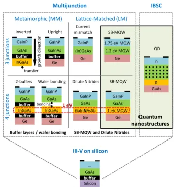
available at the beginning of the project and had demonstrated efficiencies at laboratory scale slightly above 40% [7]. With the aim of increasing this efficiency, several kinds of MJSCs have been investigated (Fig.2): we can classify them according to the number of sub-cells (3JSC or 4JSC) and to the material growth strategy: lattice-matched (LM) or metamorphic (MM). The MM approach allows for an optimal bandgap combination (current matching between subcells) to the expense of a potential degradation on material quality due to the difference in lattice constant. On the contrary, LM approach avoids material degradation to the expense of constraining the kind of materials that need to be grown to that ones with the same lattice constant than the substrate (typically germanium). This key difference determines the kind of investigations that has been carried out for each strategy: For the MM approach, the main research focused on investigating the proper intermediate buffer layers for accommodating the difference in the lattice constant. On the contrary, for the LM approach the main research focused on finding new materials lattice matched to the Ge substrate and with the desired bandgap energy. In this regard, this project focused on two kinds of materials: Multi-Quantum Wells (MQW) or Superlattices (SL) and dilute nitrides (GaInNAs). In what follows we describe each of these three approaches in detail.
2.1.1 Metamorphic structures
The use of buffer layers in the MM approaches has led to good results. Concerning upright-MM 3JSC (Fig. 2), Fraunhofer-ISE upgraded their technology [7] and increased slightly the conversion efficiency (41.4 % @ 500-600 suns AM1.5D). The anti-reflecting coating of some of these cells was optimized taking into account the secondary optical element used in Daido modules, and the cells exhibited an average efficiency of 39.5 % in the range from 400 to 1000 suns. Concerning the inverted-MM 3JSC (Fig. 2), SHARP has fabricated a world record Fig. 1: NGCPV partners: 9 Japanese and 7 Europeans, 10
Universities and 6 Companies. EU Coordinator: Universidad Politécnica de Madrid, JP Coordinator: The University of Tokyo.
buffer
Ge InGaAs
buffer
Ge
InGaAs GaInNAsSb Ge
1 eV MQW Ge
Buffer layers / wafer bonding SB-MQW and Dilute Nitrides
4
ju
n
Quantum nanostructures
…
buffer
Silicon GaAs
III-V on silicon
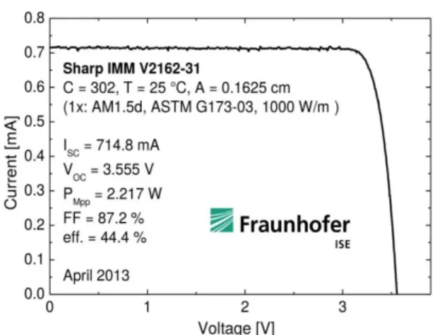
efficiency solar cell (44.4 % @ 246-302 AM1.5 D suns and 37.9 % at one sun) by the optimization of several elements in the cell structure such as reduction of the series resistance of the tunnel junction, optimization of the anti-reflective coating, optimization of the window layer of the top cell, etc. Both kinds of MJSCs have gone through reliability tests involving climatic chambers with high temperature, together with current injection of the cells at UPM. Electroluminescence experiments have also been carried out at FhG-ISE. The results suggest that both type of cells of FhG-ISE and SHARP are robust devices with expected operation lifetimes longer than 30 years [8].
Alternatively to buffer layers, the wafer bonding technique has been utilized to manufacture 4JSCs. The best result obtained within this project has been a 4JSC with 38.5 % efficiency @ 188 suns AM1.5D (FhG-ISE).
2.1.2 Lattice-matched structures: Dilute Nitrides Dilute nitrides are a kind of highly mismatched alloy in which a small fraction of nitrogen (typically less than 5%) is diluted in the semiconductor, enabling the reduction of the GaAs bandgap down to 1 eV. In these materials, the simultaneous incorporation of In is needed to compensate the lattice diminution and fabricate 1eV-band gap materials latticed matched to GaAs substrate. Thus, GaInAsN is regarded as a promising material to manufacture the 1.0 eV middle-bottom subcell in the LM-4JSC (Fig. 2).
Unfortunately, the growth of dilute nitrides is very challenging due to the appearance of N-related defects that drastically can deteriorate the material quality. Along this project, a strong effort has been devoted to the exhaustive characterization of those defects in GaAsN and GaInAsN materials [9]–[14]. For that, several advanced techniques, such as DLTS, PPT, TR-PL, etc., have been used (see section 5). From the examination of single junction GaAsN solar cell grown by Chemical Beam Epitaxy (CBE) it has been observed that the main recombination in the cell happens in the space charge region and is dominated by a non-radiative recombination center at 0.31 eV below the bottom edge of the conduction band [11]. This center has been suggested to be related with a split interstitial of a N and As atoms in a single V-site (N-As)As and has been found to be very stable, behaving as an atom in its ideal site, so that its elimination is very challenging. Works carried out within
this project have shown that both thermal annealing [13] and hydrogen irradiation [14] are effective in removing this center. As a result of this exhaustive research, the highest electron mobility of 2000 cm2/Vs in Ga(In)NAs material grown by MBE [10] was obtained, which opens the door to develop high efficient LM-4JSC.
2.1.3 Lattice-matched structures: MQW and SL MQW and SL consist of periodic nanostructures with alternating layers of at least two semiconductors (named QW and barrier material) and can be engineered to obtain a tunable effective bandgap (Fig.4). The difference between MQW and SL lies in that SL has a particularly thin barrier material (typically < 5nm) enabling carrier tunneling between adjacent layers. By using a strain-balanced (SB) structure, a variety of materials can be grown dislocation-free on Ge and GaAs substrates, so they have being investigated as subcells in the LM approach for both triple and quadruple junction solar cells (Fig.2). Particularly, NGCPV project has focused on the following two structures: (1) LM (not SB) GaInAsP/GaInP MQW for the 1.75 eV top cell in the LM-3JSC, and (2) SB InGaAs/GaAsP for both 1.20 eV (middle cell in the LM-3JSC) and 1-1.2 eV (middle-bottom cell in the LM-4JSC) materials.
Dual junction solar cells (2JSC) with a top cell comprising 40 repeats of lattice-matched GaInAsP/GaInP (fundamental transition at 1.67 eV) and a bottom cell with 50 repeats of strain-balanced InGaAs/GaAsP (fundamental transition at 1.21 eV) have been developed with an efficiency of 28% [15]. Besides, a 70-period, 1.15-eV bandgap InGaAs/GaAsP MQW solar cell has been developed as a promising material in 0.66/1.15/1.51/1.99-eV 4JSC. The device developed reached the target open-circuit voltage and over 75% of the current density required for realizing a 1.15-eV subcell in a 50%-efficient quad-junction solar cell [16]. These structures (InGaAs/GaAsP MQW) have been incorporated into a triple-junction solar cell structure (Ge/1.2eV-MQW/GaInP) by the wafer-shuttle strategy, in which monolithically integrated MJSC were created by sequential growth in different epitaxial reactors in Europe and Japan [17].
Fig. 3: Current-voltage characteristic of the world record efficiency inverted-MM solar cell fabricated by SHARP. Efficiency independently confirmed by FhG-ISE.
of the absorption coefficient related to IB to CB transitions in InAs/GaAs QDs [20]. Due to the very weak absorption, it has been determined that it is necessary the use of light management structures that increase optical length by a factor of 50 and the growth of QD structures comprising 100-300 layers in order to approach efficiencies above 40 % using InAs/GaAs structures [19]. As a means to increase the number of QD layers, strain balanced (SB) InAs/GaAs(N) QDSCs have been investigated [21]. However, due to the low bandgap of GaAsN (~1.2 eV), this structure has been found to be not optimal for single junction IBSC, and it would fit only in multijunction designs. In order to develop optimal single junction IBSC material, InAs/AlGaAs (barrier bandgap of ~1.8eV) structures have been extensively investigated. As remarkable result, due to the higher activation energy of InAs/AlGaAs QDs, these devices have demonstrated (for the first time in this project) IBSC operation at room temperature [22]. In these structures, the importance of inserting the so-called “field damping layers” has also been experimentally revealed [23]. These layers take the QDs into a flat band potential region, inhibiting any tunnel mechanism between the IB and the CB. Research in this Project has also resolved spectrally for the first time the generation of photocurrent as a consequence of photon absorption in the IB to CB transitions for both InAs/GaAs and InAs/AlGaAs devices [24], [25].
2.3 III-V on silicon
The growth of high quality III-V semiconductors on silicon substrates is a promising approach for high-efficiency, low-cost multijunction solar cells. Particularly, in this project we have investigated the growth of both GaAs and GaP on silicon. The best result was obtained for thin GaP layer (up to 150 nm) on silicon, for which dislocation densities below 106 cm-2 were obtained (Fraunhofer-ISE). The direct growth of GaAs on silicon has been investigated by irradiation with both In and Sb during the initial stages of the GaAs growth (Asahi Kasei). It has been confirmed by in-situ XRD measurement at the laboratory in Spring-8 that the rotation domain can be decreased by using In irradiation [26]. It has been also demonstrated that surface flatness and crystallinity can be drastically improved by Sb irradiation [27], [28]. The best result was obtained for a combination of a 250 nm GaAsSb buffer layer followed by 1 µm GaAs and a very thin GaAsSb/GaAs intermediate layer, just before the final 4µm GaAs growth. This buffer structure led to dislocation density as low as 5x106 cm-2 observed by plan-view TEM.
3 CPV MODULE
In order to have a cost-effective CPV system, three key aspects must be ensured: high concentration factor, efficiency and tolerance. With this goal as a target, a new type of CPV module has been developed (Fig.5) based on the Dome-shaped Fresnel Köhler (DFK) concept [29], [30] which provides extended tracking error and alignment tolerances as well as allows operating under higher concentration factors with a very high optical efficiency. This design is based in two previous successful designs: the dome-shaped Fresnel lens system developed by Daido Steel and the FK concentrator designed by UPM. The key features of this design are: high optical efficiency (~85%), a very high concentration-acceptance product (CAP) of 0.72 [30], high spatial and spectral irradiance uniformity in the cell (due to the Köhler integration), no light leakage losses [31], [32] and a very compact design, due to the low f
number. Besides, the SOE allows the encapsulation to provide an excellent cell protection, and the 4-fold scheme (Fig.5) mitigates the aging issues (due to solarization) in the SOE. These characteristics make this concentrator a robust and reliable design that enables the development of cost-effective CPV systems.
The manufacturing of the DFK concentrator involves a key issue regarding the POE molding process. The dome-shaped Fresnel lens cannot be designed with positive draft angles for the inactive facets (leading to a simple demolding process) so that a novel manufacturing process is required. Daido Steel has developed a demolding technique in which 9-part molding dies are separated from the piece in a sequence where each independent part can be demolded independently from the others. This technique has been already successfully proved in other concentrators manufactured by Daido Steel in mass-production.
Outdoor experimental characterization of these CPV modules lead to maximum efficiencies of 32.3% at CSTC (corrected by cell temperature of 25ºC) and acceptance angles of 0.98º (1000X geometrical concentration) by using commercial ~37.7% MM-3JSC. By using 39.5% Fraunhofer-ISE LM-3JSC, the measured CPV module efficiency was 31.0%. The lower module efficiency for the cells with higher efficiency is explained by the imbalance of the spectral response which highlights the relevance of wide-band optical designs [33].
several anti-soiling coating were developed by University of Miyazaki and applied to the dome-shaped Fresnel lens [34]. After 10 months of operation, the transmittance with antisoiling coating was 89%, if compared with the transmitance without coating of 83%. Furthermore, thermal coatings were applied to effectively reduce the cell temperature by ~10ºC (e.g. from 93.1ºC to 82.6ºC) [35].
4 CPV SYSTEMS
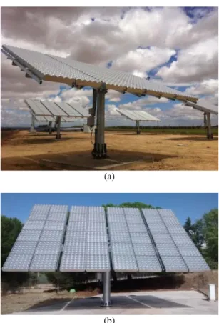
CPV system reefers to a full unit containing a number of CPV modules mounted in the tracker system. At the early stages of the project, an experimental 50 kWp CPV plant (Fig.6a) was built by BSQ and UPM in Villa de Don Fadrique (Toledo, Spain). The plant consists of 5 systems, each one comprising 48 Daido CPV modules with different configurations (back pan thickness, anti-soiling system, radiative paints, etc.). The nominal concentration of each module is 820X and uses commercial LM-3JSC. BSQ developed the tracking systems and is responsible of the operation and maintenance tasks. This plant is operative since mid-2012 and has served to provide firsthand experience in order to forecast the energy produced by a CPV system installed in a particular location, knowing the typical meteorological data in that place and the rated performance of the plant (under some standard operating conditions). For instance, it has been observed that the northern wind produces a much better cooling of the cells (35% more effective) [36]. Other aspects such as developing methods for the thermal characterization of
CPV systems without special module modification for the placement of temperature sensors have been developed [37]. Based on an exhaustive meteorological characterization (total irradiance, spectral irradiance, ambient temperature, module temperature, wind velocity and direction, relative humidity, etc.) the translating equations from standard to real operating conditions have been obtained. For that, UPM and ENEA have developed advanced software tools for analyzing the many parameters acquired.
At the end of the project, a 15kW CPV system with best performing 48 CPV modules using DFK optics and 37.7% standard industrial LM cells was developed and installed at the UPM campus (Fig. 6b). The CSOC (concentrator standard operating condition) efficiency was 27.8% measured by UPM [33] (Fig.7) which is the highest efficiency reported up to date for a full CPV system.
5 ADVANCED CHARACTERIZATION TOOLS
5.1 Characterization of novel materials and devices In this section we summarize several techniques that have been developed to characterize materials and devices for CPV applications. These include more or less conventional techniques, but also advanced techniques. Among the conventional ones we count, for example, with transmission electron microscopy (TEM), photoluminescence (PL), photo reflectance (PR), deep level transient spectroscopy (DLTS), surface photo-voltage (SPV) and time resolved photoluminescence (TR-PL). Among the advanced techniques, we count with two newly developed techniques: the three dimensional real-time reciprocal space mapping (3D-RTSM) and the piezoelectric photoconductivity (PPT). 3D-RSTM is an MBE in-situ X-ray diffraction (XRD) measurement used to characterize in real-time the lattice relaxation during the growth of lattice mismatched semiconductor layers (for instance, InGaAs on GaAs or GaAs on silicon). This equipment uses the X-ray radiation coming from the Spring-8 synchrotron facility, where the MBE is also located. PPT technique has been developed by U. Miyazaji and consists on the detection of the vibrational modes induced in a piezoelectric when the sample is illuminated; thus, it allows studying non-radiative recombination processes, for instance in GaAsN [9]. (a)
(b)
Fig. 6: (a) CPV plant at Villa de Don Fadrique (Toledo, Spain) installed by BSQ with conventional Daido modules and (b) 15 kW CPV system installed at UPM campus (Madrid, Spain) using DFK concentrator optics.
5.2 Characterization of CPV cells and modules
There are two complementary techniques for characterizing CPV cells and modules: outdoor and indoor measurements. Indoor characterization provides a controllable environment (spectrum, cell temperature, irradiance, etc.) so that it is well suited for standardization purposes and importantly, for a fast indoor rating in the industrialization of CPV components. On the contrary, outdoor measurements unveil the possible problems related with the tracking structure, as well as it allows presenting the thermal effects on the cell (or module) performance. The combination of indoor and outdoor measurements provides the most complete information and both kinds of measurements have been carried out in this project following a round-robin methodology. According to this methodology, we have compared and evaluate the results obtained by different laboratories in order to define accurate measurement techniques.
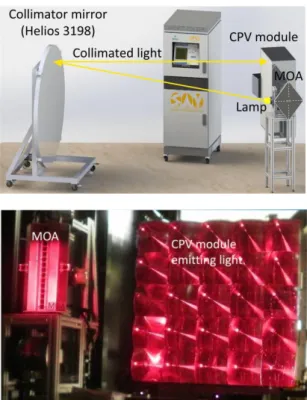
For the indoor measurements of CPV modules, the Helios 3198 solar simulator (conceived and developed by UPM and licensed to Solar Added Value S.L. in 2008) has been routinely used at several laboratories. This simulator produces a uniformly distributed light pulse on the CPV module with very similar characteristics to the sun’s light and records the I-V curve. In order to extend the functionality of this simulator, UPM has developed a new system to unveil the possible defects during the manufacturing of CPV modules. This system is denominated Module Optical Analyzer (MOA) (Fig.8) and is based on the luminescence inverse (LI) method [38]. It provides by analysis of the light emitted in luminescent mode, not only the angular transmittance function but also the misalignments between units caused by defects in the CPV module, all in few seconds. Therefore, it is suitable for characterizing CPV modules in the production line. One unit has been installed at Daido Steel factory and has been used as an extension to
the Helios 3198 simulator. This system has been found useful to detect defects in the CPV modules in the production line [39].
Several outdoor platforms are being used for testing CPV modules at different partner sites, following a round-robin scheme. In particular, CEA has developed an outdoor test facility called OSFAM (One Size Fits All Module) for testing cells under outdoor conditions. Besides, ENEA is characterizing a 6.3 kWp CPV plant installed at their site in order to develop tools for the characterization of CPV plants that can be applied to the characterization of the 50 kWp CPV plant in Spain (see Section 4).
6 SUMMARY
NGCPV project (June 2011 – November 2014) has been the first joint project between Japan and Europe to develop a new generation of concentrator photovoltaic cells, modules and systems. This paper has reviewed the main achievements of the project, among them, the attainment of a new world record efficiency for a triple junction solar cell of 44.4% (SHARP) and the attainment of the highest reported CPV overall system efficiency of 28% (under CSOC) by using an innovative CPV module design. It is also remarkable the installation of an 50 kWp CPV plant that is being used to develop accurate models to forecast the energy production of CPV plants, and the development of novel characterization tools for CPV modules, such as the MOA. Besides, a number of achievements have been obtained also in the field of material development and characterization, including quantum nanostructures for developing novel solar cell designs, novel buffers for the growth of lattice mismatched semiconductors and III-V compounds on silicon substrates, the development of wafer bonding techniques, and the fabrication and exhaustive characterization of dilute nitrides for developing 1eV material lattice matched to germanium.
7 AKNOWLEDGEMENTS
This work has been supported by the NGCPV project for EU-Japan Cooperation, funded by the European Commission (Grant 283798) and NEDO. Authors from UPM acknowledge the financial support of the Comunidad de Madrid through the Programme MADRID-PV (Grant number S2013/MAE-2780).
Fig. 8: MOA system developed to characterize CPV modules in a production line.
8 REFERENCES
[1] Solar Power Europe, “Global Market Outlook for solar power 2015-2019,” 2015.
[2] M. Yamaguchi and A. Luque, “High efficiency and high concentration photovoltaics,” IEEE
TRANSACTIONS ON ELECTRON DEVICES, vol.
46, no. 10, pp. 2139–2144, 1999.
[3] A. Luque, “Will we exceed 50% efficiency in photovoltaics?,” Journal of Applied Physics, vol. 110, no. 3, p. 031301, 2011.
[4] J. E. Haysom, O. Jafarieh, H. Anis, K. Hinzer, and D. Wright, “Learning curve analysis of concentrated photovoltaic systems,” Progress in Photovoltaics: Research and Applications, p. n/a–n/a, 2014.
[5] Fraunhofer-ISE, “Levelized cost of electricity of renewable energy technologies,” Nov. 2013.
[6] IRENA, “Renewable Energy Cost Analysis - Solar
Photovoltaics,” 2012.
[7] W. Guter, J. Schone, S. P. Philipps, M. Steiner, G. Siefer, A. Wekkeli, E. Welser, E. Oliva, A. W. Bett, and F. Dimroth, “Current-matched triple-junction solar cell reaching 41.1% conversion efficiency under concentrated sunlight,” Applied Physics Letters, vol. 94, no. 22, p. 223504, 2009.
[8] V. Orlando, P. Espinet, N. Nuñez, F. Eltermann, Y. Contreras, J. Bautista, M. Vázquez, A. W. Bett, and C. Algora, “Preliminary temperature accelerated life test (ALT) on lattice mismatched triple-junction concentrator solar cells-on-carriers,” in AIP Conference Proceedings, 2014, vol. 1616, pp. 250– 253.
[9] K. Kashima, A. Fukuyama, Y. Nakano, M. Inagaki, H. Suzuki, M. Yamaguchi, and T. Ikari, “Nitrogen related deep levels in GaAsN films investigated by a temperature dependence of piezolectric photothermal signal,” presented at the Materials Science Forum, 2012, vol. 725, pp. 93–96.
[10] N. Miyashita, N. Ahsan, M. Inagaki, M. M. Islam, M. Yamaguchi, and Y. Okada, “High electron mobility in Ga(In)NAs films grown by molecular beam epitaxy,” Applied Physics Letters, vol. 101,
no. 22, p. 222112, 2012.
[11] B. Bouzazi, N. Kojima, Y. Ohshita, and M. Yamaguchi, “Capacitance-voltage and current-voltage characteristics for the study of high background doping and conduction mechanisms in GaAsN grown by chemical beam epitaxy,” Jounal of Alloys and Compounds, vol. 552, pp. 469–474, 2012.
[12] B. Bouzazi, N. Kojima, Y. Ohshita, and M. Yamaguchi, “Analysis of Current Transport Mechanisms in GaAsN Homojunction Solar Cell Grown by Chemical Beam Epitaxy,” IEEE Journal
of Photovoltaics, vol. 3, no. 2, 2013.
[13] B. Bouzazi, N. Kojima, Y. Ohshita, and M. Yamaguchi, “Effect o Thermal Stress on a N-related Recombination Center in GaAsN Grown by Chemical Beam Epitaxy,” Japanese Journal of Applied Physics, vol. 51, p. 02BP02, 2012.
[14] B. Bouzazi, J. H. Lee, H. Suzuki, N. Kojima, Y. Ohshita, and M. Yamaguchi, “Origin Investigation of a Nitrogen-Related Recombination Center in GaAsN Grown by Chemical Beam Epitaxy,”
Japanese Journal of Applied Physics, vol. 50, p.
051001, 2011.
[15] K.-H. Lee, W. J. Barnham, J. S. Roberts, M. Fuhrer, D. Alonso-Alvarez, and N. J. Ekins-Daukes, “Dual-junction solar cells with multiple-quantum-well top cell,” presented at the CPV-9, Miyazaki, Japan.
[16] K. Toprasertpong, H. Fujii, T. Thomas, M. Führer, D. Alonso-Álvarez, D. J. Farrell, K. Watanabe, Y. Okada, N. J. Ekins-Daukes, M. Sugiyama, and Y. Nakano, “Absorption threshold extended to 1.15 eV using InGaAs/GaAsP quantum wells for over-50%-efficient lattice-matched quad-junction solar cells,”
Prog. Photovolt: Res. Appl., p. n/a–n/a, Jan. 2015.
[17] D. Lackner, S. P. Philipps, F. Dimroth, H. Sodabanlu, K. Watanabe, N. Miyashita, M. Sugiyama, Y. Okada, and A. W. Bett, “Monolithically Integrated Multi-Junction Cells built by Multiple Separate Growths in Different Epitaxy Reactors,” presented at the 6th World Conference on Photovoltaic Energy Conversion, 2014.
[18] A. Martí, E. Antolín, C. R. Stanley, C. D. Farmer, N. López, P. Díaz, E. Cánovas, P. G. Linares, and A. Luque, “Production of Photocurrent due to Intermediate-to-Conduction-Band Transitions: A Demonstration of a Key Operating Principle of the Intermediate-Band Solar Cell,” Phys. Rev. Lett., vol. 97, no. 24, p. 247701, Dec. 2006.
[19] A. Mellor, A. Luque, I. Tobías, and A. Martí, “Realistic Detailed Balance Study of the Quantum Efficiency of Quantum Dot Solar Cells,” Advanced
Functional Materials, p. n/a–n/a, 2013.
[20] A. Luque, A. Mellor, I. Ramiro, E. Antolín, I. Tobías, and A. Martí, “Interband absorption of photons by extended states in intermediate band solar cells,” Solar Energy Materials and Solar
Cells, vol. 115, pp. 138–144, 2013.
[21] P. G. Linares, E. López, I. Ramiro, A. Datas, E. Antolín, Y. Shoji, T. Sogabe, Y. Okada, A. Martí, and A. Luque, “Voltage limitation analysis in strain-balanced InAs/GaAsN quantum dot solar cells applied to the intermediate band concept,” Solar Energy Materials and Solar Cells, vol. 132, pp.
178–182, Jan. 2015.
[25] A. Datas, E. López, I. Ramiro, E. Antolín, A. Martí, A. Luque, R. Tamaki, Y. Shoji, T. Sogabe, and Y. Okada, “Intermediate Band Solar Cell with Extreme Broadband Spectrum Quantum Efficiency,” Phys. Rev. Lett., vol. 114, no. 15, p. 157701, Apr. 2015.
[26] H. Suzuki, D. Ito, A. Fukuyama, and T. Ikari, “Reduction of rotational twin formation by indium pre-evaporation in epitaxially grown GaAs films on Si (111) substrate,” Journal of Crystal Growth, vol. 380, no. 0, pp. 148 – 152, 2013.
[27] O. Morohara, H. Geka, Y. Moriyasu, and N. Kuze, “Sb irradiation effect on growth of GaAs thin film on Si (111) substrate,” J. Cryst. Growth, vol. 378,
pp. 113–116, Sep. 2013.
[28] O. Morohara, H. Geka, Y. Moriyasu, and N. Kuze, “Reducing dislocations in GaAs on Si by a novel GaAs1-x Sbx buffer layer for multi-junction solar cells,” presented at the 40th IEEE Photovoltaic
Specialists Conference, 2014.
[29] P. Zamora, P. Benitez, Y. Li, J. C. Miñano, J. Mendes-Lopes, and K. Araki, “Photovoltaic performance of the dome-shaped Fresnel-Köhler concentrator,” presented at the SPIE, 2012.
[30] P. Zamora, P. Benitez, J. C. Miñano, J. Mendes-Lopes, and K. Araki, “The dome-shaped fresnel Köhler concentrator,” presented at the CPV-8,
Toledo, Spain, 2012.
[31] P. Espinet-González, R. Mohedano, I. García, P. Zamora, I. Rey-Stolle, P. Benitez, C. Algora, A. Cvetkovic, M. Hernández, J. Chaves, J. C. Miñano, and Y. Li, “Triple junction Solar Cell Performance Under Fresnel based Concentrators Taking Into Account Chromatic Aberration And Off-axis Operation,” presented at the CPV-8, Toledo, Spain, 2012.
[32] P. Zamora, P. Espinet-González, P. Benitez, I. García, I. Rey-Stolle, J. C. Miñano, and C. Algora, “Experimental confirmation of FK concentrator intensitivity to chromatic aberrations,” presented at
the CPV-9, 2013.
[33] H. Nagai, K. Araki, K. Hobo, P. Zamora, P. Benitez, J. C. Miñano, K. Nishioka, Y. Ota, I. Luque-Heredia, J. Hashimoto, T. Ueda, Y. Hishikawa, R. Herrero, S. Askins, I. Antón, R. Nuñez, G. Sala, M. Steiner, M. Niemeyer, G. Siefer,
Coatings Technology, vol. 215, pp. 472–475, Jan. 2013.
[36] M. Castro, C. Domínguez, R. Nuñez, I. Antón, G. Sala, and K. Araki, “Detailed effects of wind on the field performance of a 50 KW CPV demonstration plant,” presented at the CPV-9, Miyazaki, Japan, 2013.
[37] R. Núñez, I. Antón, S. Askins, G. Sala, and K. Araki, “Characterization of CPV arrays based on differences on their thermal resistances,” in AIP Conference Proceedings, 2014, vol. 1616, pp. 144– 148.
[38] R. Herrero, S. Askins, C. Domínguez, I. Antón, G. Sala, K. Araki, and H. Nagai, “Evaluating Misalignements and angular transmittance function by the luminescence inverse method,” presented at the CPV-9, Miyazaki, Japan, 2013.