Jonathan E. Proesel, Senior Member, IEEE, Doug M. Gill, Christian W. Baks,
Alexander V. Rylyakov, Senior Member, IEEE, Clint L. Schow, Senior Member, OSA,
William M. J. Green, Senior Member, OSA, and Benjamin G. Lee, Senior Member, IEEE
Abstract—We propose a flexible optical transmitter for the short-reach optical interconnects that includes a silicon photonic segmented Mach–Zehnder modulator driven by a distributed six-channel 32-nm silicon on insulator (SOI) complementary metal-oxide semiconductor driver integrated circuit. Optical equalization is demonstrated to extend the bandwidth limitation of the trans-mitter with non-return to zero signaling at 25 Gb/ s. We also gener-ate four-level pulse amplitude modulation (PAM-4) signaling using the same transmitter architecture. Transmission of 46 Gb/s PAM-4 signal with bit error rate (BER) well below hard-decision forward error correction limit is experimentally demonstrated. Low driver power consumption of 130 mW at 46 Gb/ s PAM-4, corresponding to 2.8 pJ/bit power efficiency, is also achieved.
Index Terms—Distributed driver, modulator, optical intercon-nects, silicon photonics.
I. INTRODUCTION
O
PTICAL interconnects targeting both short and long reaches in intra- and inter-datacenter networks, as well as access and metro networks, have recently received an increased interest due to the tremendous growth in data traffic [1]. To address this exponential growth, high bandwidth, energy effi-cient and low cost optical transceivers are needed. While today the short-reach optical interconnects (up to 300 m) deployed inside the datacenter are dominated by low cost VCSEL-based multimode-fiber links, there is a growing demand for longer reach optical links in intra- and inter-datacenter interconnectsManuscript received July 8, 2016; revised August 23, 2016; accepted Septem-ber 5, 2016. Date of publication SeptemSeptem-ber 5, 2016; date of current version November 1, 2016.
T. N. Huynh, N. Dupuis, J. E. Proesel, D. M. Gill, C. W. Baks, W. M. J. Green, and B. G. Lee are with the IBM T. J. Watson Research Center, Yorktown Heights, NY 10598 USA (e-mail: [email protected]; [email protected]; [email protected]; [email protected]; cbaks@ us.ibm.com; [email protected]; [email protected]).
R. Rimolo-Donadio was with the IBM T. J. Watson Research Center, York-town Heights, NY 10598 USA. He is now with Costa Rica Institute of Technol-ogy, Cartago 30101, Costa Rica (e-mail: [email protected]).
A. V. Rylyakov was with the IBM T. J. Watson Research Center, Yorktown Heights, NY 10598 USA. He is now with the Coriant Advanced Technology Group, New York, NY 10016 USA (e-mail: [email protected]).
C. L. Schow was with the IBM T. J. Watson Research Center, Yorktown Heights, NY 10598 USA. He is now with the University of California at Santa Barbara, CA 93106 USA (e-mail: [email protected]).
Color versions of one or more of the figures in this paper are available online at http://ieeexplore.ieee.org.
Digital Object Identifier 10.1109/JLT.2016.2606558
(from 500 m to 10 km) for datacenter expansion or installation of new mega-datacenters [2]. The use of single-mode fiber in-frastructure operating at wavelengths in the 1.3μm transmission window for newly installed mega-datacenters, or interconnects between datacenters, open promising opportunities and also many challenges for silicon photonic integration. With the advantages of building on the long history of complementary metal-oxide semiconductor (CMOS) technology, silicon photonics would potentially provide a low cost, large scale integration, power efficient and small footprint solution [3], [4] to cope with the exponential increase in data traffic.
The modulator is a central device in optical transmitters and has attracted extensive research and development in both academia and industry over the last decade [5]. Here, we inves-tigate a flexible transmitter which includes a co-packaged seg-mented MZM and a low power 32 nm CMOS multi-channel IC driver for the next generation of optical interconnects. The flex-ibility of the transmitter is brought about by the multi-segment approach in the design of the high-speed phase shifters. The transmitter first leverages the well-known advantages of seg-mented modulators, which reduce the device capacitance seen by each driver channel by breaking the long phase shifter into many short segments, enabling extended modulation bandwidth. The multiple segments can then be employed in various manners to provide maximum extinction ratio, to perform optical equal-ization (EQ), or to provide multi-level signaling. In the case of EQ, the bandwidth may be further extended using techniques such as feed-forward equalization (FFE). Although FFE can be generated by driving a segmented modulator with an equalized driver IC, typically this requires a linear driver with significantly more bandwidth than the modulator. Alternatively, the scheme that we first demonstrated in [6] provides equalization in the optical domain while using non-linear, un-equalized drivers. Moreover the transmitter can easily be used to migrate to higher order modulation formats such as multi-level pulse amplitude modulation (PAM), or can deploy adaptive-PAM modulation formats for dynamic optical networks.
Previously segmented MZM designs were reported on the silicon platform [7] and recently on the InP platform [8] for non-return to zero (NRZ) signaling. Higher order modulation formats generated by segmented modulators were also reported such as PAM-4 in [9], [10] and 64-Quadrature Amplitude Mod-ulation (64-QAM) in [11]. In [6], we presented a transmitter
Fig. 1. Design and fabrication of the segmented modulator: (a) waveguide structure of the MZM; (b) cross-section of the rib waveguide and dimensions; (c) cross-section of the ridge waveguide and dimensions; (d) annotated die pictures of a segmented modulator having six 400μm-long segments on a 500μm pitch.
design using optical equalization and demonstrated improved BER performance of the optical link at 22 Gb/ s. In this paper, we report more details on the transmitter fundamentals and de-sign with extensive experimental results. Optical equalization performance at higher bitrates: a 25 Gb/s NRZ signal as well as BER performance of PAM-4 signals up to 46 Gb/ s, is presented. The organization of the paper is as follows: Section II discusses the design of the silicon modulator and the driver IC employed in the flexible transmitter, Section III reports the experimen-tal measurements and results for optical equalization of NRZ signaling, Section IV presents the experiments and BER perfor-mance of PAM-4 signaling, and finally, Section V concludes the paper.
II. TRANSMITTERDESIGN
In this section, we describe the design of the flexible trans-mitter that includes a six-segment silicon MZM co-packaged with a six-channel 32 nm CMOS driver IC. The assembly of the device on a printed circuit board (PCB) is then presented.
A. Segmented Mach-Zehnder Modulator
The segmented Mach-Zehnder modulator was designed and fabricated in IBM developed CMOS Integrated Nano Photonics technology CMOS9WG [4]. The MZM has a 2×2 structure using fully-etched silicon waveguides and 2×2 input and output directional couplers. Both arms of the MZM are equipped with six modulator segments of either 300 μm or 400μm and the pitch between the segments is 500μm. Each elementary segment has a ridge waveguide structure and implants on the partially etched silicon define a p-n diode, which is operated in carrier-depletion mode. More details on the p-n phase shifter structural parameters can be found in [12] and [13]. Each segment has rib-to-ridge and a ridge-to-rib waveguide transition tapers at the input and output respectively, in order to ensure a good electrical isolation between segments. The MZM also includes in each arm a 50 μm-long resistive heater that consists of a thin silicide layer embedded within a ridge waveguide. Fig. 1 presents a schematic of the MZM waveguide structure (a) as well as cross-section of the rib (b) and ridge waveguides (c). Fig. 1(d) shows annotated die pictures of a segmented modulator
Fig. 2. Circuit schematic showing one 2-Vpp driver channel.
Fig. 3. (a) Custom printed circuit board and (b) micrograph of packaged segmented modulator with driver IC.
after fabrication having six 400μm segments. The measured capacitance of each segment was 30 fF/ 100μm and the pad capacitance was about 40 fF at a−3V bias. The Vπ-L of the phase shifter was 2.04 V-cm.
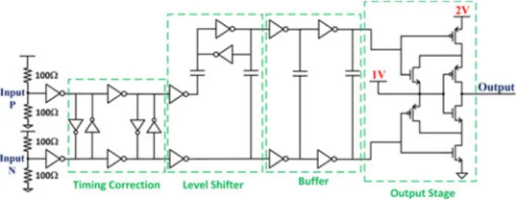
B. 32 nm CMOS Distributed Driver IC
The CMOS distributed driver IC is a 6-channel version of the IC reported in [14]. The spacing between each driver channel is 500μm, matching the pitch of the modulator segments. Fig. 2 shows the circuit design of one driver channel in the 6 × 1 array. The RF inputs have 50Ω terminations for impedance matching with standard laboratory equipment (in particular, the bit pattern generator output), followed by CMOS inverters to amplify the signal to 1 Vpp. Cross-coupled CMOS inverters minimize the timing error between the differential signals. A level shifter stage provides low (0 to 1 V) and high (1 to 2 V) CMOS outputs, which are buffered by inverter chains to drive the output stage. The output stage has a cascode configuration to limit the static voltage across any device to 1 V while providing 2-Vpp output swing. Each of the six driver circuits occupies 60 μm× 31 μm, for a total circuit area of 0.011 mm2. The driver IC is 3.4 mm×0.9 mm.
C. Transmitter Assembly
Fig. 4. Optical equalization with segmented MZM and multi-channel driver IC.
with decoupling capacitors for the modulator’s cathode bias is illustrated in Fig. 3(b).
III. OPTICALEQUALIZATIONWITHSEGMENTEDMODULATOR
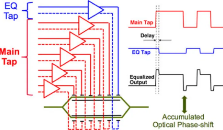
Optical FFE can be performed for NRZ signaling using the proposed transmitter design by simply employing one or more of the segments as equalizer taps. Fig. 4 illustrates the funda-mental concept utilizing the segmented modulator in a two-tap EQ scheme. The EQ tap (shown in blue) is inverted and de-layed with respect to the main tap (red). The tap weight can be discretely controlled by selecting the number of segments used for each tap, and can be in theory further optimized by adjusting the drive voltage or segment length of each tap in-dependently. Compared with the electrical equalization imple-mented within the driver IC, this optical equalization scheme can compensate for the bandwidth limitation of a linear trans-mission channel with relaxed requirements on driver linearity. By trading-off the optical extinction ratio of the transmitted sig-nal, we show that the optical EQ can provide a more open eye that yields significant improvement in receiver sensitivity and jitter compared to no equalization [6]. In this section, we ex-perimentally investigate the use of optical EQ on a segmented MZM variant with 400μm segment length at 25 Gb/s NRZ transmission.
A. Experimental Setup
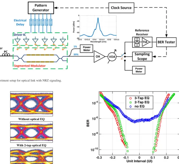
Fig. 5 depicts the diagram of the high-speed experimental setup. A multi-channel pattern generator is employed to gener-ate synchronous pseudo-random binary sequences (PRBSs) to provide driving signals to 6 channels of the driver IC. Electrical phase shifters are used to finely control the delay of the driving signals. In reality, input signal distribution can be implemented by a resistor network and buffers for delay control. The RF input signals were routed through SMP connectors on the PCB across micro-strip transmission lines and terminated into the on-chip 50Ωterminations. The differential output of each channel of the IC drives each segment of the modulator in push-pull configura-tion. DC biases are provided to the PCB through ribbon cables. As described above, the driver IC would require two level DC voltages: VD D 1 is biased at 1 V and VD D 2 is biased at 2 V. A
larization controller is placed before the modulator to optimize the polarization of light launched into the modulator. The light is edge-coupled to the silicon modulator through single-mode tapered-lensed fibers positioned with 3-axis precision stages. The inset of Fig. 5 shows the output optical spectrum from the modulator. Output light from the modulator is tapped 1% for power monitoring, while 99% passes through an optical ampli-fier (OA). Finally, an optical switch was used to select between a sampling scope with a 30-GHz photo-detector plugin, an optical average power meter, or a reference receiver (Rx), which is a commercial 43 Gb/ s receiver with integrated trans-impedance amplifier (TIA) and limiting amplifier. The differential electri-cal output signal from the receiver is then fed into the BER tester and the sampling scope. A signal generator is deployed to provide the external clock for the pattern generator, the BER tester and the scope trigger. Receiver sensitivity measurements are presented by plotting BER versus optical modulation am-plitude (OMA). The OMA axis is calibrated by the received power measured from the optical average power meter and the extinction ratio at low bitrate (5 Gb/ s). The timing margin of the NRZ signal is measured by taking bathtub curves at high OMA and extracting the jitter values from well-known jitter models. To perform optical EQ, the main tap segments are driven by the same pattern with matched delay while the EQ tap segments are driven with an inverted pattern and optimized delay. The optical coupling loss is ∼3 dB per facet, and at the quadrature point, the total insertion loss of the MZM is 6 dB.
B. Results and Discussion
We run the transmission experiment at 25 Gb/ s and explore both 2-tap and 3-tap EQ implementations. The transmitter is first operated without EQ (i.e. 1 tap), then optical EQ with 2 taps and 3 taps is tested using PRBS-7 pattern. Fig. 6 shows the optical eye diagrams. The optical eyes consistently show the decreasing in amount of inter-symbol interference (ISI) when larger degrees of equalization are applied. However, the extinction ratio of the NRZ signal is reduced with more taps. The measured extinction ratio is 7.1 dB without optical EQ, 4.9 dB with 2-tap EQ, and to 2.4 dB with 3 taps.
Fig. 5. Experiment setup for optical link with NRZ signaling.
Fig. 6. Transmitted optical eye at 25 Gb/s for 400μm-segment MZM with PRBS-7 pattern.
Fig. 8 plots the receiver sensitivity measurement results with 400μm-segment modulator at 25 Gb/ s bitrate with and without equalization. The BER versus OMA curves in Fig. 8 confirm the significant improvement in receiver sensitivity when us-ing optical equalization. Without EQ, an error floor appears at BER = 10−11 while with EQ, error free back-to-back trans-mission can be achieved with BER = 10−12at−4 dBm OMA with 2-tap EQ and −8 dBm with 3-tap EQ. As discussed above, higher degrees of equalization yield more improvement in re-ceiver sensitivity but with lower extinction ratio. An optimum operation point with 3-tap EQ has been found in this particular transmitter. As shown in Fig. 8, a 4 dB penalty at BER=10–12 is observed when reducing the number of EQ taps from 2 to 1. The power consumption of the transmitter subsystem is 143 mW including 140.6 mW from the CMOS driver IC (not includ-ing power dissipated on 50Ωinput termination) and 2.4 mW
Fig. 7. Optical equalization enlarges the time margin in the bathtub curves at 25 Gb/s for 400μm-segment MZM.
from the heaters. This yields a power efficiency of 5.7 pJ/bit at 25 Gb/ s operating bitrate. The results consolidate the advantage of low driver power consumption in CMOS technology. As a point of reference, a state-of-the-art BiCMOS driver for a sili-con photonic transmitter has been reported with 450 mW power consumption [15].
IV. PAM-4 SIGNALINGWITHSEGMENTEDMODULATOR
Fig. 8. Equalization improves the receiver sensitivity for optical link operating at 25 Gb/s with 400μm-segment MZM.
Fig. 9. PAM-4 signal generation with segmented MZM and multi-channel driver IC.
As illustrated in Fig. 9, the 4-level PAM signal can be simply generated with multi-equal-segment MZM by driving N seg-ments with the least-significant-bit (LSB) stream and 2× N segments with the most-significant-bit (MSB) stream. In this section, we report the experimental results of PAM-4 signaling with a 300μm-segment MZM without and with advanced signal processing up to 46Gb/s.
A. PAM-4 Signal Transmission Experiments
The experimental setup for PAM-4 signaling is similar to the setup for NRZ described in the previous section except for some small changes as follow. The first 2 segments of the MZM are driven by the same pattern from the LSB stream while the MSB stream drives the remaining 4 segments of the device. The MSB is derived from PRBS-7 sequence and the LSB is from the same PRBS-7 sequence with 10-bit delay to de-correlate the two bit streams forming a PAM-4 symbol sequence. All six driving signals are tuned to match the phase delay as with NRZ signaling. At the receiver side, the reference limiting receiver
Fig. 10. Transmitted optical eye at different bitrate from the 300μm-segment MZM.
for NRZ signal was replaced by a reference linear receiver with 20 GHz bandwidth. Instead of directly measuring real-time BER by a BER tester (BERT) as with NRZ signaling, the electrical signal output from the receiver is captured at 80Gsamples/s over-sampling rate by a real-time scope with 32 GHz bandwidth. The captured signal is then used for offline BER estimation.
Fig. 10 shows the optical eyes at different bitrate recorded by the sampling scope with a 30 GHz bandwidth optical plugin. The optical eyes demonstrate even-spacing between the four levels of the signal which would suggest that the modulator was well driven in the linear region around the quadrature point of the MZM transfer function. The measured extinction ratio (between level-0 and level-3 of PAM-4 signal) for 28 Gb/ s in Fig. 10(a) was 2.8 dB. At high bitrate, significant ISI degraded the vertical eye opening, especially the middle-level eye, as in Fig. 10(d). The extinction ratio of the transmitted signal could be improved by modifying the MZM design as follows: (1) increasing the length of each segment with the trade-off of in-creasing the segment capacitance, (2) inin-creasing the number of segments with accompanying increase in the number of drivers and power consumption.
B. BER Performance of PAM-4 Signaling
Fig. 11. BER performance at different MMSE tap-lengths for 40 Gb/s PAM-4 signaling with 300μm-segment MZM.
Fig. 12. BER performance of PAM-4 signaling with and without 7–tap MMSE equalizer at different bitrate for 300μm-segment MZM.
equalization filter could be added to the signal processing to im-prove BER performance with a trade-off of DSP complexity required for receiver implementation.
Fig. 11 shows the BER performance versus received op-tical power for 40 Gb/ s PAM-4 signal without and with MMSE equalization (filtering). Even without advanced DSP, the 40 Gb/ s PAM-4 signal demonstrated good BER performance, operating well below hard-decision pre-FEC (7% overhead) limit (BER = 3.8×10⁻³). The MMSE equalizer would im-prove receiver sensitivity about 2 dB at BER = 10−3. When increasing the tap-length (2N–1) of the MMSE equalizer from 7-taps to 127-taps, the BER is slightly improved. That would
suggest the 7-tap length MMSE equalizer is sufficient for this transmission link.
Fig. 12 plots the BER performance of PAM-4 signaling at different bitrates. At 46 Gb/ s, without advanced DSP, BER be-low the pFEC limit is achieved, but would require high re-ceived power, –3 dBm for BER = 10−3. The 7-tap MMSE equalizer significantly improves receiver sensitivity by 6 dB at BER = 10−3with larger BER-curve slope at this data rate. A 5.5 dB penalty at BER = 10−3could be observed when moving from 40 Gb/ s to 46 Gb/ s without DSP and is reduced to 1.5 dB penalty with 7-tap MMSE equalization. Obviously, at low bi-trate when operating well below the bandwidth limitation of the system, the benefit provided by the digital equalizer would be less (eg. 1.5 dB penalty at 28 Gb/ s). At 46 Gb/ s PAM-4, the transmitter subsystem power consumption is 130.5 mW corre-sponding to a power efficiency of 2.8 pJ/bit.
V. CONCLUSION
In this paper, we demonstrated a flexible silicon photonics transmitter using a segmented MZM. The silicon modulator was driven by a 6-channel 32 nm CMOS driver IC wire-bonded in the same package. Error free transmission at 25 Gb/ s NRZ is achieved with optical EQ. The transmitter further provides flexibility in varying the EQ’s tap weight by altering the ratio of segments devoted to main and equalizing signals. PAM-4 signal transmission at 46 Gb/ s with BER well below pre-FEC limit is also reported. The transmitter presents the ability to ef-fectively perform adaptive PAM modulation formats by simply manipulating the segment-driving scheme while exhibiting very low power consumption. The energy efficiency of the driver IC could be further improved in the future design where the chan-nels for the same bit stream would share some common amplifier stages. That shows the potential of a flexible silicon photonics transmitter for fast-reconfigurable agile optical networks.
ACKNOWLEDGMENT
The authors would like to acknowledge J. Orcutt, M. Khater, E. Kiewra, J. Rosenberg, C. Xiong, A. Stricker, J. Ellis-Monaghan, C. Reinholm, S. Chilstedt, F. Anderson, M. Nicewicz, N. Feilchenfeld, W. Haensch, and the rest of the IBM Research and Microelectronics Division teams contribut-ing to CMOS9WG Silicon Photonics technology development.
REFERENCES
[1] Cisco Visual Networking Index: Forecast and Methodology, 2015–2020. (2016). [Online]. Available: http://www.cisco.com/c/en/us/solutions/ collateral/service-provider/visual-networking-index-vni/complete-white-paper-c11-481360.html
[2] D. Mahgerefteh et al., “Techno-economic comparison of silicon photonics and multimode VCSELs,” J. Lightw. Technol., vol. 34, no. 2, pp. 233–242, Jan. 2016.
[3] C. R. Doerr, “Silicon photonic integration in telecommunications,”
Fron-tiers. Phys. vol. 3, pp. 1–16, 2015, doi: 10.3389/fphy.2015.00037.
[4] N. Feilchenfeld et al., “An integrated silicon photonics technology for O-band datacom,” in Proc IEEE Int. Electron Devices Meeting, Dec. 2015, vol. 25, pp. 25.7.1–25.7.4.
100 Gb/s PAM-4 generation,” Photon. Technol. Lett., vol. 27, pp. 2433– 2436, 2016.
[10] C. Xiong, D. Gill, J. Proesel, J. Orcutt, W. Haensch, and W. M. J. Green, “A monolithic 56 Gb/s CMOS integrated nanophotonic PAM-4 transmitter,” in Proc. IEEE Opt. Interconnects Conf., 2015, pp. 16–17.
[11] A. Aimone et al., “DAC-free ultra-low-power dual-polarization 64-QAM transmission with InP IQ segmented MZM module,”in Proc. Opt. Fiber
Commun. Conf., 2016, Paper Th5C.
[12] J. C. Rosenberg et al., “A 25 Gbps silicon microring modulator based on an interleaved junction,” Opt. Express, vol. 20, pp. 26411–26423, 2012.
[13] D. M. Gill et al., “Demonstration of a high extinction ratio monolithic CMOS integrated nanophotonic transmitter and 16 Gb/s optical link,”
IEEE J. Sel. Topics Quantum Electron., vol. 21, no. 4, pp. 212–222,
July/Aug. 2015.
[14] N. Dupuis et al., “30-Gb/s optical link combining heterogeneously inte-grated III–V/Si photonics with 32-nm CMOS circuits,” J. Lightw. Technol., vol. 33, no. 3, pp. 257–662, Feb. 2015.
[15] G. Denoyer et al., “Hybrid silicon photonic circuits and transceiver for 50 Gb/s NRZ transmission over single-mode fiber,” J. Lightw. Technol., vol. 33, no. 6, pp. 1247–1253, Mar. 2015.
[16] IEEE P802.3bs 400 Gb/s Ethernet Task Force. (2014).[Online]. Available: http://www.ieee802.org/3/bs/index.html
[17] M. Mazzini et al., “25 GBaud PAM4 error free transmission over both single mode fiber and multimode fiber in a QSFP form factor,” in Proc.
Opt. Fiber Commun. Conf., 2015, Paper Th5B.3.
[18] F. Chang et al., “Link performance investigation of industry first 100G PAM4 IC chipset with real-time DSP for data center connectivity,” in
Proc. Opt. Fiber Commun. Conf., 2016, Paper Th1G.2.
Tam N. Huynh was born in Dien Khanh, Khanh Hoa, Vietnam, in 1984. He
received the B.S. degree from Ho Chi Minh City University of Technology, Ho Chi Minh, Vietnam, in 2007, the M.Sc. and Ph.D. degrees from Dublin City University, Dublin, Ireland, in 2010 and 2014, respectively, all in telecommuni-cation engineering. He is currently a Postdoctoral Researcher at the IBM T. J. Watson Research Center, Yorktown Heights, NY, USA. His research interests include semiconductor lasers, silicon photonics, and coherent optical commu-nications.
Nicolas Dupuis received the B.S. and M.S. degrees from the Universit´e Blaise
Pascal, Clermont-Ferrand, France, and the Ph.D. degree from the Universit´e de Lorraine, Metz, France, in 2009, all in physics. He is currently a Research Staff Member at the IBM T. J. Watson Research Center, Yorktown Heights, NY, USA. Before joining IBM, he was a Postdoctoral Researcher with Bell Laboratories, Crawford Hill, NJ, USA, working on high-speed InP-based photonic circuits. His research interests include silicon photonics, optical switching, and optical link modeling.
ing and optimization of interconnects, analysis of signal and power integrity problems, and high-speed circuit design.
Jonathan E. Proesel (M’10–SM’16) received the B.S. degree in computer
en-gineering from the University of Illinois Urbana-Champaign, Champaign, IL, USA, in 2004. He received the M.S. and Ph.D. degrees in electrical and com-puter engineering from Carnegie Mellon University, Pittsburgh, PA, USA, in 2008 and 2010, respectively. In 2010, he joined the IBM T. J. Watson Research Center, Yorktown Heights, NY, USA, where he is currently a Research Staff Member working on analog and mixed-signal circuit design for optical trans-mitters and receivers. He has also held internships with IBM Microelectronics, Essex Junction, VT, USA, in 2004 and IBM Research, Yorktown Heights, in 2009. His research interests include high-speed optical and electrical commu-nications, silicon photonics, and data converters. He is a Member of the IEEE Solid-State Circuits Society and the IEEE Circuits and Systems Society. He received the Analog Devices Outstanding Student Designer Award in 2008, the SRC Techcon Best in Session Award for Analog Circuits in 2009, and core-ceived the Best Student Paper Award for the 2010 IEEE Custom Integrated Circuits Conference.
Doug M. Gill received the Ph.D. degree in materials science program from
University of Wisconsin, Madison, WI, USA, in 1994, working on Er-doped LiNbO3, and was a Research Associate at Northwestern University during 1995–1998 working on thin-film electrooptic modulators, optical amplifiers, and nonlinear polymers. From 1999 to 2011, he was a Member of Technical Staff at Alcatel-Lucent Bell Labs, working on research and development of 40 Gb/s LiNbO3 modulators, CMOS compatible photonics, hybrid-integrated transceivers, and advanced transmission formats for cost-effective data trans-port. Since 2011, he has been a Research Staff Member at IBM T. J. Watson Research Center, Yorktown Heights, NY, USA, working on electrooptic sys-tems monolithically integrated within CMOS electronics. He received the New-port Research Award, two Central Bell Labs Teamwork Awards for work on 40 Gb/s ultra-long haul DPSK systems and the DARPA funded EPIC program on CMOS compatible photonics, was inducted into the Alcatel-Lucent Techni-cal Academy in 2010, and holds more than 30 patents and 70 refereed journal and conference articles.
Christian W. Baks received the B.S. degree in applied physics from Fontys
Alexander V. Rylyakov (SM’15) received the M.S. degree from Moscow
In-stitute of Physics and Technology, Dolgoprudny, Russia, and the Ph.D. degree from State University of New York (SUNY) at Stony Brook, Stony Brook, NY, USA, in 1989 and 1997, respectively, both in physics. From 1994 to 1999, he worked with the Department of Physics, SUNY Stony Brook on integrated circuits based on Josephson junctions. From 1999 to 2014, he was a Research Staff Member with the IBM T. J. Watson Research Center, Yorktown Heights, NY, USA, working on integrated circuits for wireline and optical communica-tion, and on digital phase-locked loops. In 2015, he joined Coriant Advanced Technology Group as an Electronics Team Lead.
Clint L. Schow (SM’10) received the Ph.D. degree in electrical engineering
from the University of Texas at Austin, Austin, TX, USA, in 1999. He joined IBM, Rochester, MN, USA, assuming responsibility for the optical receivers used in IBMs optical transceiver business. From 2001 to 2004, he was with Agility Communications, Santa Barbara, CA, USA, developing high-speed op-toelectronic modulators and tunable laser sources. In 2004, he joined the IBM T. J. Watson Research Center, Yorktown Heights, NY, USA, as a Research Staff Member and currently manages the Optical Link and System Design Group responsible for optics in future generations of servers and supercomputers. He has directed multiple DARPA-sponsored programs investigating chip-to-chip optical links, nanophotonic switches, and future systems utilizing photonic switching fabrics. He has published more than 150 journals and conference articles and has16 issued patents. He is a Senior Member of the OSA.
William M. J. Green (M’03–SM’13) received the B.Sc. degree in engineering
physics from the University of Alberta, Edmonton, AB, Canada, and the Ph.D. degree in electrical engineering from the California Institute of Technology, Pasadena, CA, USA, in 2005. He is currently the Manager of the Silicon Inte-grated Nanophotonics Group at the IBM Thomas J. Watson Research Center, Yorktown Heights, NY, USA. His primary research activities include design and enablement for optical devices and integrated optical-electronic systems in support of next-generation high-speed optical interconnects. In addition, he has investigated the silicon photonic integrated circuit platform for nonlinear optical generation and processing of midinfrared optical signals, for various applications in molecular spectroscopy, environmental sensing, and medical diagnostics. He received several Awards including the 2012 IBM Corporate Award, and the 2012 IEEE Photonics Society Young Investigator Award. He has served on the technical organizing committees for numerous OSA and IEEE conferences. He is a Senior Member of the OSA.
Benjamin G. Lee (M’04–SM’14) received the B.S. degree from Oklahoma