Towards a new generation of solar cells: silicon supersaturated with
titanium or vanadium.
E. Garcia-Hemme , R. Garcia-Hernansanz , J. Olea , D. Pastor , A. del Prado , I. Mártil , P. Wahnón , G. González-Díaz
Abstract:
Introduction:
Silicon has been the key material since the beginning of the solar photovoltaic era. However, in the race for the competitiveness of the photovoltaic industry, new solar cells concepts and materials has been studied and obtained. In a delicate equilibrium between reducing fabrication costs and enhancing the solar cells efficiency, different approaches have been implemented. For example, with the objective of reducing fabrication costs, quaternary semiconductor materials synthetized since low cost / earth abundant materials as CuZnSnS/Se are being used as absorbers materials in thin film photovoltaic cells with very promising results.1 By the side of enhance the solar cell efficiency, lab examples of multi-junction cells have demonstrated performance over 43%.2 However, this efficiency is gained at the cost of increased complexity and manufacturing price. Then, a third generation of solar cells is up to come in order to meet this delicate equilibrium between production costs and conversion efficiencies.
The intermediate band (IB) solar cell is a representative concept of this third generation of solar cells.3 The concept was first proposed in 1997 and since then an important work has been dedicated to describe its physical properties and to fabricate practical devices that can demonstrate its operational principles.
An IBSC is based on an IB material. This new material consist of a semiconductor with its conduction and valence band, but a new energy band of allowed states takes place within the semiconductor bandgap. With this scheme, this kind of material would be able to take advantage of sub-bandgap photons to promote charge carriers from the valence band to the IB and from the IB to the conduction band. This extra photocurrent would be added to that given by transition VB - CB leading to an increase in the photo-generated current and higher conversion efficiencies.
To attain these goals, several approaches are now in progress at different laboratories worldwide. Si supersaturated with chalcogens prepared by laser irradiation in SFé atmosphere has exhibited strong sub gap absorption.4 Photodetectors build-up with Si highly doped with S and Se by means of ion implantation and subsequently pulsed laser melted (PLM) have shown extended infrared photoresponse below the Si bandgap with high gain levels.5 In previous papers, we have shown that Si supersaturated with Ti by ion implantation and then PLM treated shows unusual optoelectronic characteristics. " Electrical transport properties of these materials have been well explained for both Ti concentrations below and above the insulator-metal transition, also known as Mott transition.9
Once this limit is achieved, the reduction of the NRR is possible and an increase of the charge carrier lifetime may take place, as explained in the configuration diagram theory.11
As we have proved recently by means of lifetime measurements, Ti supersaturated Si samples have exhibited lifetime recovery, in agreement with the previous arguments.14 These results demonstrated that once the Mott transition is achieved, the derealization of the states associated to the impurities occurs and the so-called intermediate band (IB) is formed at this supersaturated region. More recently, we have proved again the lifetime recovery of these samples by means of spectral photo response measurements.15
In this work, we present the photoelectronic and structural characteristics of Si supersaturated with vanadium (V) or titanium (Ti). V and Ti are a well-known deep
1 f\ 17
center in Si ' and, as a consequence, a possible candidate to form an IB under adequate experimental conditions.
Experimental:
Samples lxl cm in size of n-type Si (111) with a thickness of 300 um (p~200 9 1 1 1 % "X
Qcm, n~1500 c n r V V1, n~2 .2x10 cm" at room temperature) were implanted at 32 keV with V at two different doses (1013 and 1016 cm"2) and with Ti in a double implantation process (1015 cm'2 at 35 keV plus 4xl015 cm"2 at 150 keV) using a 7° tilt angle. Subsequently the implanted samples were PLM processed at 1 Jem"2 for V and 1.8 Jem" for Ti, with a KrF excimer laser (248nm) at IPG Photonics. Also, some Si samples were implanted with Si at 170 keV and 10 cm" dose and subsequently processed by PLM at 1 Jem" . We have chosen 170 keV for the Si implanted Si samples because our objective is to obtain a more defective and thicker layer after the implantation and PLM process for comparative purposes.
To analyze the V and Ti depth profile, time-of-flight secondary ion mass spectrometry (ToF-SIMS) measurements were carried out in a ToF-SIMS IV model manufactured by ION-TOF, with a 25 keV pulsed Bi3+ beam at 45° incidence. A 10 keV voltage was used to extract the secondary ions generated and their time of flight from the sample to the detector was measured using a reflection mass spectrometer. The structural characterization of the samples was carried out by transmission electron microscopy (TEM) and electron diffraction (ED) patterns obtained with a Titan3 G2 working at 300 keV.
Results and Discussions:
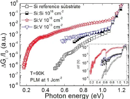
As the fabrication of V or Ti supersaturated Si is intended for solar cell applications, one of its key properties is the spectral photoresponse. Fig. 1 shows the
results of the sheet conductance increase under illumination (—-j normalized to the
incident light power 70, as a function of the incident photon energy. The sheet conductance increase is directly related to the increase of the charge carrier concentrations with respect to the darkness equilibrium state, as it was previously shown in Ref. 15: AGD = qiiLnt, where q is the electron charge, ¡J. is the charge carrier
mobility, An is the charge carrier concentration increase due to the illumination and t is
the sample thickness. The —- is presented for the V implanted samples at 1013 and 1016
A)
cm"2 doses and PLM at 1 Jem"2 and the Si implanted sample at 1016 cm"2 dose and PLM at 1 Jem"2. We have chosen two different V concentrations well below and above the theoretical Mott limit to clearly observe the possible effect related to the insulator-metal transition. Also, a reference silicon unimplanted substrate is presented for comparative purposes. In order to observe the different levels of the electrical noise for the different samples, the inset in Fig. 1 shows the AC voltage (darkness voltage - illumination voltage) measured directly by the lock-in amplifier. Due to the high noise, —- is not
represented below 0.6 eV for the V implanted sample at 1013 cm"2 and 0.7 eV for the Si implanted Si sample.
For all the samples we can observe the abrupt increase of the —- magnitude for A)
photon energies over 1.1 eV, corresponding to the intrinsic charge carrier generation due to the Si band to band transitions. Concerning the Si reference substrate, we observe a minor photoresponse for infrared photon energies. This infrared photoresponse has been well explained in terms of carrier generation due to surface states.18'19
10u
io-
1io-
210 3
10 4
- 10 5
< ] 10 6
IO"7
10 8
0.2 0.4 0.6 0.8 1.0 1.2
Photon energy (eV)
Fig. 1 Increase of the sheet conductance spectral response normalized to the impinging light power density as a function of the incident photon energy for the Si unimplanted reference
sample, for the V implanted Si samples at IO13 and 1016 cm"2 doses and the Si implanted Si sample at IO16 cm'2 dose. Implanted samples were subsequently PLM processed at 1 Jem'2. Inset shows the AC voltage measured as a consequence of the chopped light that impinges the samples. Measurements were carried out at 90 K.
order of magnitude higher than the Si reference sample at 1 eV photon energy and almost 4 orders of magnitude higher at 0.5 eV photon energy. Its response is extended
deep into the infrared region, presenting an abrupt front of —- for energies starting
below 0.2 eV. Moreover, the noise level is remarkably lower than in the sample implanted at 10 cm" dose, and comparable to the noise level of the Si reference substrate. All these characteristics (electrical noise and different levels of photoresponse) will be discussed in the following paragraphs.
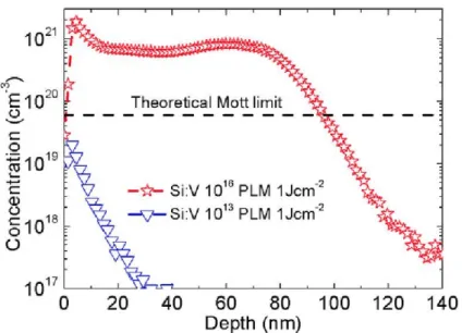
Fig. 2 shows the ToF-SIMS measurements of the V implanted with the lowest dose (10 cm" ) and the higher dose (10 cm"). For the 10 cm" implanted dose, the Mott limit concentration (6x1019 cm"3) is not reached. However the sample implanted at IO16 cm"2 dose presents a V concentration over the theoretical Mott limit in a layer of about 100 nm. Therefore, according to the Mott transition theory, two different scenarios have been obtained as a function of the implanted dose, which explains the photoconductivity measurements shown in Fig. 1. In the case of the sample implanted at 10 cm" dose we have obtained a layer that presents a high V concentration which is below the theoretical Mott limit, and possibly the insulator-metal transition has not been achieved. Therefore, the observed infrared photoresponse of this sample is mainly due to V deep levels introduced in the Si lattice as it has been previously observed for iron deep levels in Si or Zn deep levels in Si. Additionally, these V deep level impurities would act as an important source of localized recombination centers, increasing the
T=90K
PLM at 1 Jem
T ' 1 ' 1 ' 1 ' 1 ' r
Fig. 2 ToF-SIMS profiles of V implanted Si samples at 1013 and 1016 cm"2 subsequently PLM processed at 1 Jem"2.
electrical noise due to the recombination processes, " which could explain the measurements for this sample in Fig. 1. In contrast, the sample implanted with the 1016 cm" dose shows a V concentration over the theoretical Mott limit in a 100 nm thick layer. For this sample the theoretical derealization transition point has been surpassed and we could expect a reduction of the NRR processes at the V implanted layer. This reduction of the recombination processes could be related with the remarkable decrease of the electrical noise observed in the photoconductivity measurements of this sample (Fig. 1). Therefore, this result is consistent with the derealization transition of the deep level impurities in the implanted layer. Moreover, surpassing the derealization transition limit would imply the formation of a band of allowed states within the Si bandgap. The formation of this band would result in an increase of both the charge carrier lifetime and the absorption coefficient, due to sub-bandgap optical transitions involving this extra band. Both mechanisms would lead to an increase of the photoresponse, being the influence of the absorption coefficient dominant near the optical transition edge. The intense increase of the photoresponse observed for the
1 & O
sample implanted at a 10 cm" V dose (Fig. 1), together with the presence of an abrupt photoresponse edge, is consistent with the presence of delocalized states within the Si gap. Therefore, we suggest that the observed photoconductivity may be related to carrier transitions involving the CB or the VB and the allowed states derived from the derealization of the V deep levels.
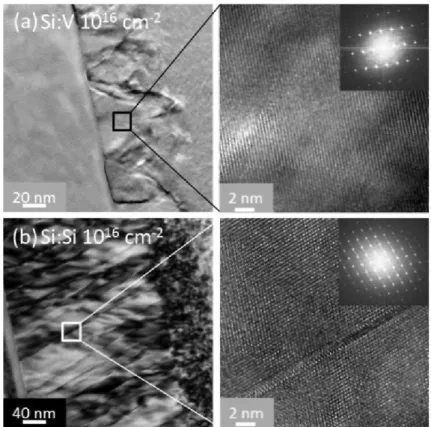
Fig. 3 Cross sectional TEM-HRTEM images and ED patterns of (a) the V implanted Si sample at 1016 cm"2 dose and (b) the Si implanted Si sample at 1016 cm"2 dose, and subsequently processed by PLM at 1 Jem"2,
comparison, Fig. 3 (b) shows the Si implanted Si sample at 10 cm" dose and PLM at 1 Jem" . Also high resolution TEM images and ED patterns are presented for both samples.
1 (\ *J
implanted sample at 10 cm" has shown a perfect crystalline structure without differences with a Si reference substrate.
The different degrees of recrystallization that these samples present are directly related with the photoconductivity measurements of Fig. 1. In the case of the Si
implanted Si, the structural defects observed in Fig. 3 (b) could contribute to both the increase of the photoresponse, as it was previously observed in Si irradiated with electrons or neutrons in order to produce structural defects, and to the increase of the electrical noise due to the crystal disorder.24 However, the high photoresponse observed
1 f\ O
in the V implanted sample at 10 cm" dose cannot be explained in terms of structural defects, since the most defective sample (Si implanted Si sample) shows a much lower
h '
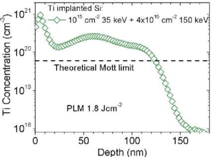
Regarding the double implanted Ti sample, Fig 4 shows the Ti concentration depth profile. The sample shows a Ti concentration over the theoretical limit to form an IB in a layer of 120 nm. Therefore for this sample we could expect a reduction of the
8
NRR processes at this 120 nm layer. Concerning the structural quality, in Ref. we can observe the high crystal quality obtained for this sample.
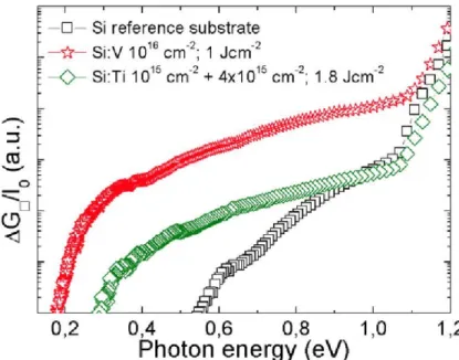
Figure 5 shows the spectral photoconductance for the Ti double implanted sample, the V implanted sample at the highest dose and a Si reference substrate. If we compare the Ti implanted sample with the V implanted sample we can observe that both samples shows a remarkable increase of the photoconductivity over the unimplanted Si reference sample. Also, both samples show an abrupt edge of the photoconductivity for the lower photons energies. However, this abrupt edge begins at different energy positions, i.e. at 0.18 eV for the V implanted sample and at 0.3 eV for the Ti implanted sample. Taking in mind that both samples present impurities concentration over the
Depth (nm)
Fig 4 ToF-SIMS profiles of Ti double implanted Si samples at 1015 and 4xl015 cm"2
o
<
0,2 0,4 0,6 0,8 1,0 1,2
Photon energy (eV)
Fig 5 Variation of the spectral photo-response as a function of the incident photon energy for the reference Si, and for the V and Ti implanted samples at different doses and PLM process.
theoretical limit to form an IB, we could relate these two sharp edges of the photoconductivity with optical transitions involving the VB and the CB with the IB. Finally, this hypothesis suggests that the IB energy position within the Si bandgap depends on the implanted element. These results are very interesting since imply we are able to engineer the photo-electronics properties of these Si based IB materials.
Conclusions:
V or Ti supersaturated Si samples have been obtained by means of ion implantation and PLM processes. Samples were implanted with two different V concentrations, below and above the theoretical metal-insulator transition limit and with a double implantation Ti process over the theoretical limit to form the IB material. As the V concentration increases, an important increase of the photoresponse is observed for the far infrared region of the spectrum as well as an important reduction of the electrical noise. The infrared photoresponse of the V or Ti supersaturated Si samples exhibits a photoconductivity edge at different energy positions. These photoresponse cannot be related with defects associated with the ion implantation nor with the PLM process, since a more defective Si implanted Si sample presents a lower infrared photoresponse and a higher level of electrical noise. We have related the high intensity
and far extended infrared photoresponse of the V sample implanted at 10 cm" dose and the Ti double implanted sample with the predictions of the delocalization of the deep levels associated with the V and Ti once the Mott limit concentration has been surpassed. This delocalization leads to a reduction of the NRR processes, which in turn is related to the reduction of the electrical noise and the formation of a band of allowed states in the Si bandgap. Therefore, an increase of both the charge carrier lifetime and
- f i i i i i
-D Si reference substrate - # - S i : V 1 01 6c m "2; 1 Jem"2
the absorption coefficient as a consequence of sub-bandgap optical transitions involving this extra band takes place. These results could lead to the development of a future generation of Si solar cells with enhanced conversion efficiencies in the far infrared region of the spectrum.
Acknowledgements:
Authors would like to acknowledge the CAÍ de Técnicas Físicas of the Universidad Complutense de Madrid for the ion implantations and metallic evaporations, the Nanotechnology and Surface Analysis Services of the Universidad de Vigo C.A.C.T.I. for ToF-SIMS measurements and the Instituto de Nanociencia de Aragón for the TEM images. This work was partially supported by the Project NUMANCIA II (Grant No. S-2009/ENE/1477) funded by the Comunidad de Madrid. Research by E. Garcia-Hemme was also supported by a PICATA predoctoral fellowship of the Moncloa Campus of International Excellence (UCM-UPM). J. Olea and D. Pastor thanks Professor A. Marti and Professor A. Luque for useful discussions and guidance and acknowledge financial support from the MICINN within the program Juan de la Cierva (JCI-2011-10402 and JCI-2011-11471), under which this research was undertaken.
References:
1. A. Fairbrother, E. Garcia-Hemme, V. Izquierdo-Roca, et al. Journal of the American Chemical Society 134, 8018-8021 (2012).
2. RR. King, NH. Karam, JH. Ermer, et al. IEEE Photovoltaic Specialist Conference, 998-1001 (2000).
3. A. Luque and A. Marti, Phys. Rev. Lett. 78 (26), 5014-5017 (1997).
4. C. H. Crouch, J. E. Carey, J. M. Warrender, M. J. Aziz, E. Mazur and F. Y. Genin, Applied Physics Letters 84, 1850-1852 (2004).
5. A. J. Said, D. Recht, J. T. Sullivan, J. M. Warrender, T. Buonassisi, P. D. Persans and M. J. Aziz, Applied Physics Letters 99, 073503 (2011).
6. J. Olea, M. Toledano-Luque, D. Pastor, G. Gonzalez-Diaz and I. Martil, Journal of Applied Physics 104, 016105 (2008).
7. J. Olea, G. Gonzalez-Diaz, D. Pastor, I. Martil, A. Marti, E. Antolin and A. Luque, Journal of Applied Physics 109, 8 (2011).
8. J. Olea, Á. del Prado, D. Pastor, I. Mártil and G. González-Díaz, Journal of Applied Physics 109, 113541 (2011).
9. N. F. Mott, Advances in Physics 21, 785-823 (1972).
10. C. H. Henry and D. V. Lang, Physical Review B 15, 989-1016 (1977).
11. A. Luque, A. Marti, E. Antolin and C. Tablero, Physica B-Condensed Matter
12. D. Pastor, J. Olea, A. del Prado, E. Garcia-Hemme, R. Garcia-Hernansanz and G. Gonzalez-Diaz, Solar Energy Materials and Solar Cells 104,159-164 (2012).
13. M. T. Winkler, D. Recht, M.-J. Sher, A. J. Said, E. Mazur and M. J. Aziz, Physical Review Letters 106, (2011).
14. E. Antolin, A. Marti, J. Olea, D. Pastor, G. Gonzalez-Diaz, I. Martil and A. Luque, Applied Physics Letters 94, (2009).
15. E. Garcia-Hemme, R. Garcia-Hernansanz, J. Olea, D. Pastor, A. del Prado, I. Martil and G. Gonzalez-Diaz, Applied Physics Letters 101, (2012).
16. T. Sadoh, H. Nakashima and T. Tsurushima, Journal of Applied Physics 72, 520-524 (1992).
17. A. Rohatgi, J. R. Davis, R. H. Hopkins, P. Rai-Choudhury, P. G. McMullin, and J. R. McCormick, Solid-State Electron. 23,415 (1980).
18. C. Goletti, G. Bussetti, P. Chiaradia and G. Chiarotti, Journal of Physics-Condensed Matter 16, S4289-S4300 (2004).
19. W. Muller and W. Monch, Physical Review Letters 27, 250 (1971).
20. H. Indusekhar and V. Kumar, Physica Status Solidi a-Applied Research 95, 269-278 (1986).
21. A. C. Wang, L. S. Lu and C. T. Sah, Physical Review B 30 , 5896-5903 (1984). 22. L. K. J. Vandamme, leee Transactions on Electron Devices 41, 2176-2187 (1994).
23. W. A. Beck, Applied Physics Letters 63, 3589-3591 (1993).