Effect of patterned coupled optical micro cavities in two dimensional Si ZnO hybrid photonic structure
6
0
0
Texto completo
(2) 7 CONGRESO INTERNACIONAL DE INGERÍA FÍSICA. Effect of patterned coupled optical micro-cavities in twodimensional Si-ZnO hybrid photonic structure V M Carrillo-Vázquez, J G Murillo Centro de Investigación en Materiales Avanzados S.C. Miguel de Cervantes 120, Complejo Industrial Chihuahua, C. P. 31109, Chihuahua, Chih., México. E-mail: [email protected] Abstract. The optical characterization of the Si-ZnO hybrid photonic device fabricated and studied in this work revealed its ability to selectively enhance the reflectance on specific wavelengths in the border of VIS-NIR range. This ability was attributed to the coupling of the embedded micro-cavities in the photonic crystal. The results found suggest the presence of a photonic band gap around the border of VIS-NIR range in the hybrid photonic structure studied.. 1. Introduction Photonic crystals (PhC) have demonstrated to be a good alternative to control the flow of light to develop new technology. Its interest have been growing incredibly every year since they were found as promising solutions for specific areas of study such like telecommunications [1-4] and light extraction on LEDs [5] for cite some of them. Two dimensional (2D) photonic crystals are of particular interest since many fabrication methods are currently available for this kind of structures like chemical assisted ion beam etching (CAIBE), reactive ion etching (RIE) and focused ion beam (FIB) milling [6, 7], among others. In this work a two-dimensional hybrid PhC was fabricated on a silicon (Si) substrate coated with a zinc-oxide (ZnO) thin film. The PhC was directly milled over the Si-ZnO hetero-structure using the FIB fabrication method. The photonic structure was described by circular air columns in square lattice and an array of 16 coupled quasi-circular micro-cavities embedded in the photonic crystal body. Reflectance measurements at normal incidence carried out on this photonic device revealed reflectance selectivity for wavelengths in the border of VIS-NIR ranges. 2. Sample fabrication In order to fabricate the sample, a silicon substrate was coated with a ~240 nm thick ZnO thin film deposited by the Assisted Chemical Vapor Deposition (AACVD) method [9]. The hybrid PhC was milled directly on the Si-ZnO hetero-structure on a large area of 84 x 84 μm2 using a Focused Ion Beam system. The photonic crystal milled showed a lattice constant a=1.05 μm and circular air columns of radius r=0.57a.The main parameters of the photonic crystal described above were 295.
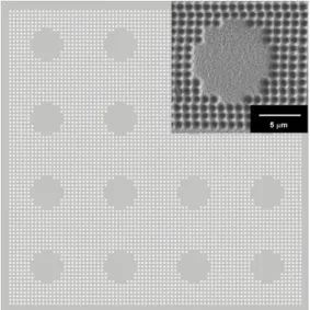
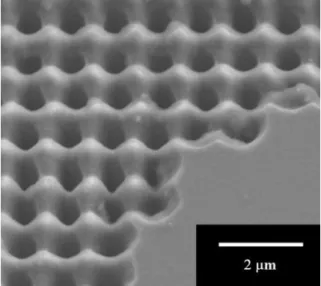
(3) 7 CONGRESO INTERNACIONAL DE INGERÍA FÍSICA achieved by setting a dose of 200 nC/μm2 and 1000 pA of irradiating current during 15 seconds per single hole using the spot milling shape. A pattern of 16 quasi-circular micro-cavities of about 10 μm in diameter and a lattice constant of ~20 μm was embedded in the photonic crystal describing a secondary square lattice. The sample was designed including a pattern of micro-cavities in which each cavity has dimensions in the next order of magnitude compared to those of the regular square lattice photonic crystal. This was to identify whether these micro-cavities can be coupled between them to induce a photonic band gap in the PhC. Also, the square lattice pattern was selected with the aim in find a complete band gap when including the micro-cavities by measuring reflectance at normal incidence since this structure is well known to show partial band gaps for transversal electric (TE) or transversal magnetic (TM) modes [8]. Redeposition of eroded material was observed during the FIB milling process driving a rough surface on the photonic crystal area as result. Figure 1 shows the design of the complete photonic crystal structure and a single microcavity of the PhC device can be observed in the inset.. Figure 1. Design of the hybrid PhC with 16 patterned micro-cavities embedded in the PhC body. Inset: SEM micrograph of single optical micro-cavity. 3. Experimental details Optical characterization of the hybrid photonic crystal was performed by measuring the optical reflectance at normal incidence using a similar experimental set up as used by Stumpf et al in Ref [10]. In order to measure reflectance on the photonic crystal two light sources as probe light were used: a He-Ne laser emitting at 633 nm and a multichannel fiber coupled laser source which emits 785, 852, 1310 and 1550 nm wavelengths. These wavelengths were used with the aim in identify the optical properties of the hybrid photonic hetero-structure in a discrete broad spectra on VIS-NIR ranges. The ZnO thin film was removed from the substrate surface once reflectance measurements were completed on the hybrid photonic crystal. Figure 2 shows a close view of the photonic structure after ZnO thin film removal where it can be observed the PhC topography that has been predicted in previous theoretical investigations for FIB fabrication method [11].. 296.
(4) 7 CONGRESO INTERNACIONAL DE INGERÍA FÍSICA. Figure 2. Micrograph of PhC on bare silicon after ZnO thin film removal in close view.. In the optical characterization of the sample both polarizations of light TE and TM modes were considered. In fact, the results of optical reflectance obtained for both polarizations were very similar, showing only very small differences between them. This finding was expected due to the PhC symmetry which determines that the light at normal incidence observes the same pattern on the photonic crystal surface for either TE or TM modes. The optical characterization of the heterostructure showed a high reflectance level on the hybrid photonic crystal area at the border of VISNIR range wavelengths and a low level for NIR wavelengths. Particularly, reflectance measurement carried out at the border of VIS-NIR range showed that level obtained for 852 nm was higher than level measured at 633, 785, 1310 and 1550 nm on the hybrid photonic crystal as depicted in Figure 3. The optical characterization was repeated on the PhC remaining on bare Si in order to determine the ZnO thin film contribution on the optical properties of the hybrid PhC. Figure 3 also shows the reflectance measurements of the PhC after the ZnO thin film removal. Here, it is noticeable that the reflectance magnitude was almost constant in the photonic structure on bare silicon for all the probe wavelengths 633, 785, 852, 1310 and 1550 nm. Furthermore, it was observed that the reflectance level of the photonic crystal on bare silicon only provides a uniform small gain compared to reflectance measured for uniform silicon substrate. Continuous dotted line in figure 3 represents the reflectance measured, using a Varian Cary 5000 spectrophotometer, on plain Si-ZnO substrate as a reference.. 297.
(5) 7 CONGRESO INTERNACIONAL DE INGERÍA FÍSICA. Figure 3. Reflectance measurement at 633, 785, 852, 1310 and 1550 nm wavelengths in PhC before and after ZnO thin film removal. Reflectance of silicon substrate and Si-ZnO hetero-structure are included for comparison purposes.. 4. Discussion It was observed a peak reflectance level at 852 nm probe wavelength in the hybrid PhC. Therefore, the hybrid photonic structure enhanced selectively wavelengths in the border of VIS-NIR ranges rather than NIR wavelengths. Moreover, reflectance measurements on the photonic crystal in bare silicon showed a constant reflectance level which was increased uniformly for all wavelengths probed in the border of VIS-NIR ranges compared to the reflectance measured for plain silicon substrate. This indicates that photonic crystal with embedded micro-cavities pattern fabricated on bare Si substrate did not contributed in the reflectance modulation as the hybrid Si-ZnO photonic crystal did. Hence, the role of ZnO thin film in the photonic hetero-structure was relevant for the optical behavior here obtained. It was noticeable that the whole hetero-structure system, i.e. the PhC with embedded micro-cavities milled on Si-ZnO, is coupled to selectively enhance the reflectance around 852 nm. This finding strongly suggests the presence of a photonic band gap around this wavelength in the hybrid photonic crystal studied in this work. Further experimentation has to be completed to confirm this statement sweeping in a continuous way a region around the border of VIS-NIR wavelengths.. 298.
(6) 7 CONGRESO INTERNACIONAL DE INGERÍA FÍSICA 5. Conclusions It has been confirmed that the hybrid photonic crystal discussed in this work was able to promote the magnitude of reflectance at the border of VIS-NIR wavelengths range. This finding suggests the presence of a photonic band gap around the border of VIS-NIR ranges for this hybrid PhC. Furthermore, it is concluded that ZnO thin film coating on the photonic hetero-structure clearly improves the reflection in this silicon based photonic crystal promoting a photonic band gap appearance.. References [55] Robinson S and Nakkeeran R 2012 Optik 123 451– 457 [56] Yang D, Tian H and Ji Y 2011 Sensor Actuat. A 171 146– 151 [57] Esmaieli A and Ghayour R 2012 Photonics Nanostruct 10 131–139 [58] Rahmati A T and Granpayeh N 2011 Optik 122 502–505 [59] Zhmakin A I 2011 Phys. Rep. 498 189–241 [60] Krauss T F and De La Rue R M 1999 Prog. Quant. Electron. 23 51-96 [61] Nellen P M, Callegari V and Bronnimann R 2006 Microelectron. Eng. 83 1805–1808 [62] Hillebrand R, Hergert W and Harms W 2000 Phys. Status Solidi (b) 217, 981 [63] Amézaga-Madrid P, Antúnez-Flores W, Ledezma-Sillas J E, Murillo-Ramírez J G, SolísCanto O, Vega-Becerra O E, Martínez-Sánchez R and Miki-Yoshida M 2011 J. Alloy Compd. 509S, S490–S495 [64] Stumpf W C, Asano T, Kojima T, Fujita M, Tanaka Y and Noda S 2010 Phys. Rev. B 82 075119 [65] Han J, Lee H, Min B and Lee S J 2010 Microelectron. Eng. 87 1–9. 299.
(7)
Figure

Documento similar
Here, we present a portable, low-cost and user-friendly photonic device integrating fluidic and optical components for the rapid processing of large sample volumes and in
In the present study, a hyperspectral imaging system was used to capture the spectral reflectance of in-vivo maxillary anterior teeth in order to characterize the color
Similar reasons could be behind other inverse relations between the internal and external border effects in other industries (like the energy & water, ceramics, pharmaceutical
van der Meulen, J. Single-photon emission by semiconductor quantum rings in a photonic crystal. Controlling the properties of single photon emitters via the purcell effect.
The process of fabrication of high quality factor photonic crystal microcavities in slabs of InP with light emission at
4 Active optical materials based on transparent glass-ceramics doped with rare-earth (RE) ions are considered promising materials for photonic applications.. The
The scope of this Thesis is the investigation of the optical properties of two systems based on semiconductor nanostructures: InAs/GaAs quantum rings embedded in photonic
We have analyzed the dynamics of a set of quantum emitters (two-level systems) whose ground state-excited state transition couples to the modes of a photonic lattice, which acts as
