Research Article
Characterization of the Manufacturing Processes to Grow
Triple-Junction Solar Cells
N. A. Kalyuzhnyy,
1V. V. Evstropov,
1V. M. Lantratov,
1S. A. Mintairov,
1M. A. Mintairov,
1A. S. Gudovskikh,
1,2A. Luque,
1,3and V. M. Andreev
11Ioffe Physical-Technical Institute of the Russian Academy of Sciences, Polytechnicheskaya Street 26,
Saint Petersburg 194021, Russia
2Saint-Petersburg Academic University, Nanotechnology Research and Education Centre RAS, Hlopina Street 8/3,
Staint Petersburg 194021, Russia
3Technical University of Madrid, Spain
Correspondence should be addressed to N. A. Kalyuzhnyy; [email protected] and V. M. Andreev; [email protected]
Received 12 December 2013; Revised 31 March 2014; Accepted 5 April 2014; Published 5 May 2014
Academic Editor: Niyaz Mohammad Mahmoodi
Copyright © 2014 N. A. Kalyuzhnyy et al. This is an open access article distributed under the Creative Commons Attribution License, which permits unrestricted use, distribution, and reproduction in any medium, provided the original work is properly cited.
A number of important but little-investigated problems connected with III-V/Ge heterostructure in the GaInP/GaInAs/Ge multijunction solar cells grown by MOVPE are considered in the paper. The opportunity for successfully applying the combination of reflectance and reflectance anisotropy spectroscopy in situ methods for investigating III-V structure growth on a Ge substrate has been demonstrated. Photovoltaic properties of the III-V/Ge narrow-band subcell of the triple-junction solar cells have been investigated. It has been shown that there are excess currents in the Ge photovoltaic p-n junctions, and they have the tunneling or thermotunneling character. The values of the diode parameters for these current flow mechanisms have been determined. The potential barrier at the III-V/Ge interface was determined and the origin of this barrier formation during MOVPE heterogrowth was suggested.
1. Introduction
Multijunction (MJ) solar cells (SCs) grown by metal-organic vapor phase epitaxy (MOVPE) demonstrate the highest effi-ciency being one of the most successful trends of photovoltaic development [1–4]. Stacking several junctions with different band gaps allows reducing significantly the fundamental losses due to charge carrier thermalization. Triple-junction cells based on the Ga0.52In0.48P/Ga0.99In0.01As/Ge structure are currently the main part of the mass production of high efficiency multijunction solar cells. Although the material combination in terms of band gap does not give the maxi-mum theoretical efficiency for triple-junction cells, the fact that they are lattice matched allows producing such mono-lithic heterostructure solar cells with a perfect crystalline quality.
The MJ SCs are widely used both in space and in terrestrial concentrator photovoltaic systems due to high
efficiency under concentrated sunlight and high radiation resistance.
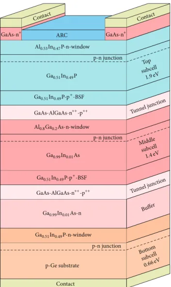
In the topological sense, the MJ SC structure is a series connection of single-junction subcells. Each subcell includes not only the photoactive p-n junction but also the functional heterolayers (e.g., window, back surface field (BSF), etc.). Moreover the subcells are connected by tunnel junctions with additional heterointerfaces. As a result, a MJ SC has a quite complicated structure (seeFigure 1), consisting of many layers with different types of interfaces including chemically dissimilar III-V/Ge interface (the GaInP/Ge heterostruc-ture is used as the bottom subcell of the triple-junction GaInP/GaInAs/Ge SC). There are a number of important but little-investigated problems connected with this interface. First of all the electrical properties of the III-V/IV interface have not been enough studied so far, especially taking into account the diffusion processes, which take place during the Ge p-n junction formation during the MOVPE growth of
Contact
Contact Contact
p-n junction
p-n junction p-n junction ARC
Al0.53In0.47P-n-window
GaAs-n+ GaAs-n+
Ga0.51In0.49P
Middle
subcell
1.4eV
Top
subcell
1.9eV
Ga0.51In0.49P-p+-BSF
Al0.8Ga0.2As-n-window
Tunnel j unction
Tunnel j unction Ga0.99In0.01As
Buffer
Ga0.51In0.49P-p+-BSF
Ga0.99In0.01As-n
Ga0.51In0.49P-n-window
p-Ge substrate
Bottom
subcell
0.66eV
GaAs-AlGaAs-n++-p++
GaAs-AlGaAs-n++-p++
Figure 1: Schematic structure of a GaInP/GaInAs/Ge triple-junc-tion solar cell.
III-V semiconductors on the Ge wafer. The interface phenom-ena may affect the charge carrier transport in the Ge subcell as well as in the whole multijunction solar cell.
In this paper a review of a number of results devoted to III-V/Ge heterostructure formed during MOVPE is pre-sented. Also new approaches to control the epitaxial het-erogrowth of III-V semiconductors on the germanium wafer during the MOVPE growth are shown.
2. Materials and Methods
The growth experiments have been performed in a horizontal low pressure R&D MOVPE reactor. Hydrogen was used as a carrier gas. The following metalorganic compounds were used as the third group element sources: trimethylgallium (TMGa), trimethylaluminum (TMAl), and trimethylindium (TMIn). Arsine (AsH3) and phosphine (PH3) were used as the fifth group element sources. Doping precursors for inves-tigated epitaxial layers were disilane (SiH4) and diethylzinc
(DEZn). The experimental layers for in situ investigations as well as photovoltaic structures were grown on 2-inch in diameter substrates.
The MOVPE installation is equipped with a UV-trans-parent quartz window for optical in situ measurements. A commercially available spectrometer has been used for performing reflectance (R) as well as reflectance anisotropy (RA) signals on rotating samples.
According to Aspnes et al. [5], the reflectance anisotropy for cubic crystals is the difference in reflectance between the two surface symmetry axes along [110] and [−110] directions. For the (100) surface, the RA signal is defined by
Δ𝑅
𝑅 = 2
𝑅110− 𝑅−110
𝑅110+ 𝑅−110, (1)
where 𝑅110 and 𝑅−110 are the complex reflectance for the polarizations parallel to the [110] and [−110] directions.
The difference in the reflection coefficients for light polarized along the main crystalline axes results mainly from the surface anisotropy [6] (taking into account the bulk symmetry of cubic crystals). This anisotropy is characterized by the spatial configuration of the dimmers formed due to surface dangling bonds. Reflectance anisotropy spectroscopy (RAS) allows picking out weak signals of the surface optical transitions using polarization properties.
Due to sample rotation in MOVPE, the RA signal mea-surement is more complicated especially when it is accom-panied by some degree of wobble [7]. Direct measurements during MOVPE growth processes give the absolute value of the RA signal that should be taken into account in analyzing experimental results.
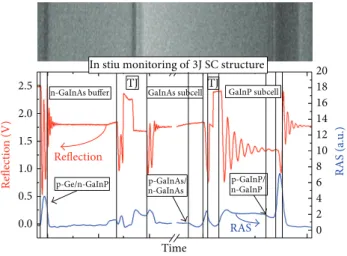
In stiu monitoring of3J SC structure
n-GaInAs buffer TJ GaInAs subcellTJ GaInP subcell
p-Ge/n-GaInP p-GaInAs/
n-GaInAs
p-GaInP/ n-GaInP
RAS Reflection
Reflec
tio
n (V)
2.5
2.0
1.5
1.0
0.5
0.0
Time
RAS (a.u
.)
20 18 16 14 12 10 8 6 4 2 0
Figure 2: Approach of the in situ control of MJ SC parameters (layer thicknesses, solid solution composition, doping levels and homoint-erface detection, heterointhomoint-erface quality, etc.) based on simultaneous measurements of the time dependencies of short-wavelength (on 3.8 eV) RA and long-wavelength (on 2.1 eV) reflection signals (lower part) and SEM image of cross-section of GaInP/GaInAs/Ge MJ SC.
III sublattice of GaInP [18], which results in narrowing the semiconductor band gap, can be determined by RAS at growth temperature of GaInP on both Ge and GaAs substrates [16].
A general method for the in situ control of MJ SC parameters (layer thicknesses, solid solution composition, doping levels, heterointerface quality, etc.) based on these studies has been proposed (Figure 2). The method is a combination of reflectance with the RAS, and it is based on simultaneously measuring the time dependence of the long-wavelength reflection signal and the short-wavelength anisotropic reflection signal [16, 19]. On the one hand the long-wavelength (on 2.1 eV) measurements characterized by the larger absorption depth allow obtaining the quite large number of Fabry-Perot oscillations on the reflection, which is useful for composition, growth rate, and thickness of a material determination. On the other hand there is direct dependence of the Δ RAS (difference between signals for doped and undoped layersΔRAS= Δ𝑅/𝑅doped−Δ𝑅/𝑅undoped)
on the logarithm of the free charge carrier concentration for the short-wavelength range, so 3.8 eV RA signal mea-surements allow controlling the doping level and observing homointerfaces. Also it is used for determining the quality of interfaces.
There is a wide range of ex situ techniques used for III-V interface characterization. The structural properties of interfaces can be studied by XRD [21]. The values of the recombination rate at interfaces can be measured using time resolved photoluminescence [22]. The values of the valence band offset (Δ𝐸𝑉) and the interface charge density at interfaces can be obtained by CV profiling [23] among other methods.
However, there are a number of methods which are helpful but not often used for this purpose. First of all they are the above mentioned optical in situ methods, which allow estimating the heterogrowth quality. As an ex situ method, the admittance spectroscopy is helpful enough for studying the interface properties [24]. In general, capture and emission of charge carriers at and from interface states lead to variation of charge at the interface and, therefore, may contribute to the structure capacitance. This fact allows one to use the admittance spectroscopy for defect characterization in the space charge regions [25] and at heterointerfaces [26].
Also the helpful experimental approach is the study of heterointerface influence on the charge carrier transport by means of the dark IV characteristics’ measurements in a wide temperature range and analysis of diode parameter temperature dependence.
For detailed study of III-V/Ge heterostructure, the experi-mental approach consisting in “subcell” fabrication is applied. The p-n junction in the Ge substrate was formed due to the diffusion of P atoms from the growing GaInP nucleation layer. Such grown heterostructure completely reproduces the narrow gap Ge subcell in MJ SC. A n++ GaAs contact layer was grown for subsequent fabrication of the test Ge photovoltaic convertor. Then an additional postgrowth ther-mal treatment which is reproducing the growth conditions (temperature and growth time) of GaInP/GaInAs wide-band-gap tandem was carried out. The structures were annealed in the AsH3atmosphere in order to prevent degradation of the GaAs cap layer.
Thus, the experimental simulation of the Ge subcell was performed by an additional thermal treatment of a single Ge cell. Such structures are referred to as “subcell” here.
3. Results and Discussion
To form the bottom Ge subcell, the epitaxial GaInP layers grown on the Ge substrate are used as the source for doping impurities (P) to form Ge p-n junction and as a wide-band-gap window for the Ge subcell. On the one hand the III-V/Ge interface is a very critical issue from epitaxial viewpoint, because it is a boundary between chemically dissimilar materials. On the other hand properties of diffusive p-n junction are less controlled and require detailed study.
There is a major problem connected with the growth of defect-free III-V semiconductors on a nonsimilar (group IV) germanium substrate. By using the RAS in situ method, the most optimal conditions for the growth of perfect III-V layers on a Ge were determined. The conditions of deoxidation of Ge substrates and the suppression of autodoping by germa-nium of the photoactive parts of MJ SC [15] structure have been found due to single-wavelength RA signal temporal dependence measurement during the growth process.
−2 0 2 4
1.6 2.0 2.4 2.8 3.2 3.6 4.0 4.4
−1.0
−0.5
0.0
7e19
5e16
2e18
5e18
1e18
SI n-type (Si) p-type (Zn)
Energy (eV)
ΔR
/R
(
10
−3
)
Tgr= 600∘C
ΔR
/R
do
p
ed
−Δ
R
/R
undo
p
ed
(
10
−3
)
Figure 3: RA spectra (upper part) andΔRAS spectra (Δ𝑅/𝑅doped−Δ𝑅/𝑅undoped) for p-type: Zn (blue) and n-type: Si (red) doped Ga0.99In0.01As layers at 600∘C growth temperature; energies near the critical points of dielectric function are marked by vertical black lines.
2000 3000 4000
Time (s)
Ge autodoping
n-GaInP/n-GaInAs interface
|Δ
R/
R|
/
(
10
−3
)
(a)
220 240 260 280 300
0 3 6 9 12 15 18 21
Growth condition optimisation
n-GaInP/n-Ge interface
Time (s)
|Δ
R
/R
|/
(
10
−3
)
(b)
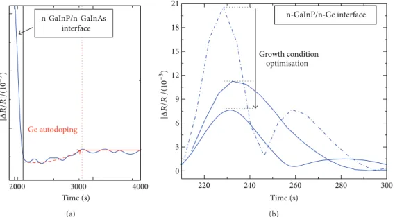
Figure 4: The in situ record of the single-wavelength (3.8 eV) RA signal: (a) during GaInAs buffer growth (Ge autodoping suppression is shown) and (b) during GaInP on Ge nucleation (optimization interface quality is shown).
The red dotted line in Figure 4(a) marks the growth time (interval of about 1000 seconds) after which the dop-ing level comes to saturation corresponddop-ing to the dopdop-ing level of the n-Ga0.99In0.01As buffer. Taking into account the Ga0.99In0.01As layer growth rate (8.5 ˚A/s) one can conclude that the thickness of the layer, when autodoping with germa-nium influences on RA signal level, is in the range 0.7–0.9𝜇m.
(a)
(b)
Figure 5: Bright field TEM image of (1–10) cross-section of a SC structure (a) and dark field TEM image of (1–10) cross-section of the GaInP/Ge interface (b). The TEM images were obtained in two-beam condition with a diffraction vector𝑔 = (002).
Further growth of a bulk semiconductor structure resulted in imperfect crystallization of the epitaxial layers. This has been confirmed by comparison of the short-wavelength reflectance signal recorded in the single-wavelength mode with a successful run.
The minimum relative value of the RA signal at the GaInP2/Ge interface achieved was 8. In this case, the reflec-tion signal level remained unchanged during the following growth of the bulk crystal. A high structural quality of the GaInP layers and a sharpness of the GaInP/Ge interface were confirmed by TEM study (Figure 5). No dislocations or any growth related defects were observed.
Thus, the approach with in situ measurements allows determining the key parameters for successful nucleation on Ge substrates including those which are difficult to obtain by means of ex situ methods.
In spite of such quality a number of new phenomena associated with a GaInP/Ge heterostructure were found during investigation by means of a number of approaches.
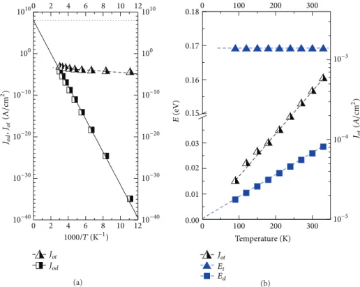
In particular, it has been shown [28, 29] that there are excess current components, which, at reverse bias, gave the saturation current density in the range of (10−4-10−3) A/cm2 for Ge p-n junction formed during the MOVPE diffusion process. Previously, it was believed that, in the Ge p-n junctions, the forward current flow mechanism is diffusion (the ideality factor𝐴𝑑= 1).
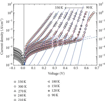
For such “subcells” (Ge subcell structure and their growth conditions were experimentally simulated as described above) the dark forward and reverse IV curves were analyzed for the temperature range of 90–330 K. The approximation of Ge subcell IV curves by means of only one-exponential (diffusion) model in the whole temperature range was not absolutely accurate. It was shown that an excess current should be taken into account for Ge subcells and that the appropriate model for approximation of IV curves is two-exponential. As a result of the diode parameter analysis, the nature of the excess current was determined as either tunneling or thermotunneling.
−0.1 0.0 0.1 0.2 0.3 0.4 0.5 0.6 0.7
Voltage (V)
101
100
10−1
10−2
10−3
10−4
10−5
10−6
101
100
10−1
10−2
10−3
10−4
10−5
10−6
C
u
rr
en
t den
si
ty (
A
/cm
2)
330K 90K
330K
300K
270K
240K
210K
180K
150K
120K
90K
Figure 6: Forward and reverse dark IV characteristics of a Ge “subcell” at different temperatures (from 90 to 330 K). Symbols are the experimental data: red line: the calculations by the two-exponential model, blue line: the diffusion components (𝐴𝑑 = 1), and blue separated line: the tunneling components (𝐸𝑡= 0.17V).
A number of samples (especially after high temperature treatment) showed “not classic” IV curves in whole tempera-ture range (Figure 6). For these samples the approximation of the forward branch of the IV curves by the sum of the components of exponential form (2) has shown that, in the operation temperature range of 90–330 K, the forward current consists of the diffusion component and the excess component:
𝐽 = 𝐽𝑜𝑑⋅ [exp(𝑉 − 𝐽 ⋅ 𝑅𝑠
𝐸𝑑 ) − 1] + 𝐽𝑜𝑡⋅ [exp(𝑉 − 𝐽 ⋅ 𝑅𝐸 𝑠
𝑡 )] ,
(2)
where 𝐽is the current density in the external circuit, 𝑉is voltage,𝑅𝑠 is the series resistance of the device, 𝐽𝑜𝑑 is the saturation current of the diffusion component (preexponent), 𝐽𝑜𝑡 is the preexponent (“saturation” current) of the excess (tunneling) component, 𝐸𝑡 is the characteristic potential of the tunneling component, and 𝐸𝑑 is the characteristic (thermal) potential of the diffusion component, which may be expressed through the ideality factor𝐴𝑑= 1:
𝐸𝑑=𝑘𝑇 𝑞 ⋅ 𝐴𝑑=
𝑘𝑇
𝑞 , (3)
where𝑞is the electron charge,𝑘is the Boltzmann constant, and𝑇is the absolute temperature.
0 2 4 6 8 10 12
0 2 4 6 8 10 12
1010
100
10−10
10−20
10−30
10−40
1010
100
10−10
10−20
10−30
10−40
Jod
,
Jot
(A
/
cm
2)
Jot
Jod
1000/T(K−1)
(a)
0 100 200 300
0 100 200 300
0.00 0.01 0.02 0.03 0.15 0.16 0.17 0.18
Temperature (K)
Jot
(
A/
cm
2 )
10−3
10−4
10−5
Jot
Et
Ed
E
(eV)
(b)
Figure 7: Dependencies of the Ge “subcell” diode parameters of diffusion (𝐸𝑑,𝐽𝑜𝑑) and tunneling (𝐸𝑡,𝐽𝑜𝑡) current components on the value of inverse (a) and forward (b) absolute temperature.
coefficient is𝑏 = Δln𝐽𝑜𝑡/Δ𝑇 = 3 ÷ 9 × 10⁻³K−1)(Figure 7). That allows characterizing the mechanism as a tunneling current.
However, in most cases, the excess component is not observed in the dark IV characteristics of Ge subcell at RT. However, at lower temperatures (especially at𝑇 < 200K) excess current has been detected. Thus, in this case the dark IV characteristic of a Ge “subcell” can be described by two-exponential model similarly to (2):
𝐽 = 𝐽𝑜𝑑⋅[exp(𝑉 − 𝐽 ⋅ 𝑅𝑠
𝐸𝑑 ) − 1] + 𝐽𝑜𝑡𝑡⋅[exp(
𝑉 − 𝐽 ⋅ 𝑅𝑠 𝐸𝑡𝑡 )] ,
(4)
where the second term is thermotunneling current, 𝐽𝑜𝑡𝑡 is the preexponent (“saturation” current), and 𝐸𝑡𝑡 is the characteristic potential of the thermotunneling component.
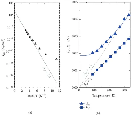
Temperature dependence of 𝐽𝑜𝑡𝑡 (Figure 8(a)) at low temperatures is rather weak (in comparison with the thermal activation dependence) but at high temperatures can be approximated by an exponential function:
𝐽𝑜𝑡𝑡= 𝐽∞⋅exp( −𝐸𝑔0
𝐴𝛽⋅ 𝑘𝑇) , (5)
where𝐸𝑔0 = 0.78eV [20] is the extrapolated value of the Ge bandgap at𝑇 → 0,𝐴𝛽is the coefficient (“ideality factor”) independent of temperature and approximately equal to 1.5, and𝐽∞is the constant, which characterizes𝐽𝑜𝑡𝑡 at1/𝑇 → 0 (experimentally determined value of𝐽∞is 5000 A/cm2).
The characteristic potential𝐸𝑡𝑡at high temperatures can be well approximated by a function which increases linearly with temperature (Figure 8(b)):
𝐸𝑡𝑡= 𝐴𝛽⋅ 𝑘𝑇
𝑞 . (6)
Thus, in this case the excess current has thermal activa-tion dependence of𝐽𝑜𝑡(with activation energy𝐸𝑎 = 𝐸𝑔/𝐴𝛽 and ideality factor𝐴𝛽 = 𝐸/(𝑘𝑇/𝑞) ∼1.5) at high tempera-tures 𝑇 ⪆ 200K, but the current acquires the tunneling character, when temperature is decreasing (𝐸𝑡𝑡0 = 0, 016 ÷ 0, 019V) (Figure 8). The availability of both the tunnel and the thermoinjection parts on 𝐽𝑜𝑡𝑡(𝑇) dependence allows characterizing the mechanism as thermotunneling.
Although the influence of thermotunneling current on the efficiency at RT and high temperature (concentrator application) can be neglected, the two-exponential model is more accurate for description of current transport in Ge subcell (formed by MOCVD) into the wide temperature range.
The nature of the excess currents cannot be explained by dislocations (as it is known for heterojunctions) because of high quality of the GaInP2/Ge interface (Figure 5). A possible reason for the excess currents was investigated in detail in our paper [30].
0 2 4 6 8 10 12
107
102
10−3
10−8
10−13
10−18
10−23
10−28
Jott
(A
/
cm
2)
A 𝛽=
1.5
1000/T(K−1)
(a)
0 100 200 300
0.00 0.01 0.02 0.03 0.04 0.05
Temperature (K) A𝛽
=1.5
Ett
Ed
Ad= 1 Ed
,
Ett
(eV)
(b)
Figure 8: Dependencies of the Ge “subcell” diode parameters of thermotunneling (𝐸𝑡𝑡,𝐽𝑜𝑡𝑡) current component and thermal potential (𝐸𝑑) of the diffusion current on the value of inverse (a) and forward (b) absolute temperature.
0.5 0.6 0.7 0.8 0.9 1.0 5.0 5.5 6.0
0.001 0.01 0.1 1
Ge subcell
GaInP/GaAs/Ge triple-junction
cells
Voltage (V)
1(100K)
3(100K)
2(110K)
C
u
rr
en
t (A/cm
2)
Figure 9: Dark IV curves recorded in a current control mode for the Ge “subcell” structure at 100 K (1) and 110 K (2), GaInP/GaAs/Ge triple-junction solar cell at 100 K (3).
increases with temperature decrease (from 0.78 V at 110 K to 0.9 V at 100 K for Ge “subcells”).
The admittance spectroscopy was applied for study of the GaInP/Ge heterointerface. The “subcell” structure exhibits a
0
0
80 120 160 200 240 280 320
Temperature (K)
×10−7 ×10⁻⁷
2
1
1.5
1
0.5
G/
𝜔
(F/cm
2)
C
apaci
ta
nce (F/cm
2 )
1kHz–1MHz
Figure 10:C-T-𝜔andG/𝜔-T-𝜔curves for GaInP/Ge subcell het-erostructures [20].
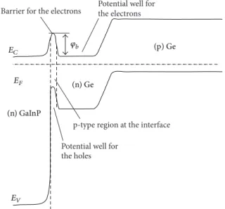
The experimental IV curves and the admittance spec-troscopy data indicate [30] the presence of the undesirable potential barrier for majority of charge carriers in “subcell” heterostructures. The origin of this barrier formation could be related to the diffusion process at the GaInP/Ge interface. In fact, simultaneously with phosphorous (V group atom) diffusion from GaInP to the Ge wafer, which forms the n-type region of the p-n junction in p-Ge, gallium and indium diffusion to Ge also exists. As Ga and In are acceptor impurities for Ge, they could form a p-type region. The diffusion coefficient of phosphorous (∼ 2.4 × 10⁻¹¹cm2/s) at growth temperature is much higher compared to that of both gallium (∼3.5 ×10⁻¹³cm2/s) and indium (∼5.9×10⁻¹³cm2/s) [31]. That causes deeper diffusion of phosphorous into the Ge wafer. However, the solubility limit of Ga in Ge (4.5 × 1020cm−3) is significantly higher than that of phosphorous (5 × 10¹⁹) cm−3 [32,33]. Therefore a local concentration of Ga atoms diffused to Ge at the GaInP/Ge interface could be significantly higher compared to that of P atoms, which leads to a narrow region with a p-type doping domination. The inversion of the conduction type in this region near the interface causes the potential barrier for electrons, which can affect the charge carrier transport properties of a Ge solar cell. The schematic band diagram with the potential barrier at the n-GaInP/n-Ge interface was proposed for the “subcell” structures (Figure 11). The behavior of the experimental IV curves and admittance spectra was reproduced by the numerical simulations using the proposed model with a 60 nm thick p-type Ge (3 × 1017cm−3) layer introduced at the interface between the (n)GaInP and (n)Ge, which forms the potential barrier of about 0.1 eV.
The dark IV curves at 100 K and 300 K for the het-erostructures with (“subcell”) and without potential barrier at the GaInP/Ge interface were simulated (Figure 12) using the AFORS-HET software [34].
The simulations have shown a good agreement with experimental data meaning that the presence of the potential barrier for electrons at the GaInP/Ge interface can explain the observed behavior at low temperatures for the “subcell” structures.
The undesirable potential barrier for majority of charge carriers at the n-GaInP/n-Ge heterointerface seems to be a general problem of the III-V/IV heteroepitaxial interfaces.
4. Summary
The review of important but little-investigated problems connected with III-V/Ge heterostructure in the GaInP/ GaInAs/Ge multijunction solar cells grown by MOVPE is presented. Experimental in situ and ex situ investigation approaches are analyzed.
A combination of reflectance and reflectance anisotropy spectroscopy in situ methods has been applied for inves-tigating III-V semiconductor growth on Ge substrates. By means of the in situ methods, the conditions for high-quality material growth on Ge substrates have been found. The growth parameters of III-V buffer layer (Ga0.99In0.01As)
p-type region at the interface Barrier for the electrons Potential well for the electrons
Potential well for the holes EC
𝜑b (p) Ge
EF (n) Ge
EV (n) GaInP
Figure 11: Schematic band diagram at equilibrium proposed for Ge “subcell” structures.
0.0 0.1 0.2 0.3 0.4 0.5
Simulation for the structures Experimental data Without barrier
With barrier
Voltage (V)
C
u
rr
en
t (A)
300K
100K
100
10−2
10−4
10−6
10−8
10−10
Figure 12: The simulated IV curves for the heterostructures with and without a potential barrier at the GaInP/Ge interface at 300 and 100 K.
for preventing autodoping by Ge of the photoactive MJ SC structure have been established.
character. The values of the diode parameters for both current flow mechanisms have been determined.
The presence of the potential barrier at the n-GaInP/n-Ge interface has been confirmed by the admittance spectroscopy, low-temperature dark IV curve measurements, and numeri-cal simulations. The origin of this barrier formation could be related to the parasitic diffusion of III group atoms into Ge substrate during heterostructure growth.
Conflict of Interests
The authors declare that there is no conflict of interests regarding the publication of this paper.
Acknowledgments
The authors want to acknowledge that this work has been supported by the Contract no. 14.B25.31.0020 from the Russian Ministry of Education and Science (Resolution no. 220). The authors thank A. A. Usikova and A. V. Malevskaya for preparation of the samples by photolithography.
References
[1] M. A. Green, K. Emery, Y. Hishikawa, W. Warta, and E. D. Dunlop, “Solar cell efficiency tables (version 41),”Progress in Photovoltaics: Research and Applications, vol. 21, no. 1, pp. 1–11, 2013.
[2] R. R. King, D. Bhusari, D. Larrabee et al., “Solar cell generations over 40% efficiency,”Progress in Photovoltaics: Research and Applications, vol. 20, no. 6, pp. 801–815, 2012.
[3] M. Wiemer, V. Sabnis, and H. Yuen, “43.5% efficient lattice matched solar cells,” inHigh and Low Concentrator Systems for Solar Electric Applications VI, vol. 810804 ofProceedings of SPIE, San Diego, Calif, USA, September 2011.
[4] R. R. King, D. C. Law, K. M. Edmondson et al., “40% efficient metamorphic GaInP/GaInAs/Ge multijunction solar cells,”Applied Physics Letters, vol. 90, no. 18, Article ID 183516, 2007.
[5] D. E. Aspnes, J. P. Harbison, A. A. Studna, and L. J. Flo-res, “Application of reflectance difference spectroscopy to molecular-beam epitaxy growth of GaAs and AlAs,”Journal of Vacuum Science & Technology A, vol. 6, no. 3, pp. 1327–1332, 1988.
[6] J.-T. Zettler, M. Pristovsek, T. Trepk et al., “Response of the surface dielectric function to dynamic surface modifications: application of reflectance anisotropy spectroscopy and spectro-scopic ellipsometry,”Thin Solid Films, vol. 313-314, pp. 537–543, 1998.
[7] P. Kurpas, M. Arens, D. Gutsche, E. Richter, and M. Weyers, “Growth monitoring of GalnP/GaAs heterojunction bipolar transistors by reflectance anisotropy spectroscopy,”Journal of Crystal Growth, vol. 195, no. 1–4, pp. 217–222, 1998.
[8] G. B. Stringfellow,Organometallic Vapor-Phase Epitaxy: Theory and Practice, Academic Press, San Diego, Calif, USA, 2nd edition, 1999.
[9] D. E. Aspnes and A. A. Studna, “Anisotropies in the above-band-gap opticalspectra of cubic semiconductors,”Physical Review Letters, vol. 54, pp. 1956–1959, 1985.
[10] V. L. Berkovits, L.F. Ivantsov, V. a. Kiselev et al., “Polarization spectra of optical transitions at a clean GaAs (110) surface,”
Journal of Experimental and Theoretical Physics Letters, vol. 41, p. 551, 1985.
[11] V. L. Berkovits, V. N. Bessolov, T. N. L’vova, V. I. Safarov, R. V. Khasieva, and B. V. Tsarenkov, “Fermi-level movement at GaAs(001) surfaces passivated with sodium sulfide solutions,”
Journal of Applied Physics, vol. 70, no. 6, pp. 3707–3711, 1991. [12] H. Tanaka, E. Colas, I. Kamiya, D. E. Aspnes, and R. Bhat, “In
situdetermination of free-carrier concentrations by reflectance difference spectroscopy,”Applied Physics Letters, vol. 59, no. 26, pp. 3443–3445, 1991.
[13] P. Wolfram, E. Steimetz, W. Ebert, B. Henninger, and J.-T. Zettler, “Growth of InGaAsP/InP-laser structures monitored by using RAS techniques,”Journal of Crystal Growth, vol. 248, pp. 240–243, 2003.
[14] K. Haberland, M. Zorn, A. Klein et al., “In-situ determination of interface roughness in MOVPE-grown visible VCSELs by reflectance spectroscopy,”Journal of Crystal Growth, vol. 248, pp. 194–200, 2003.
[15] N. A. Kalyuzhnyy, V. M. Lantratov, S. A. Mintairov et al., “In-situ monitoring during mocvd growth of the triple-junction GaInP/Ga(In)As/Ge solar cells,” in Proceedings of the 23th European Photovoltaic Solar Energy Conference (EPSEC ’08), pp. 803–810, Valencia, Spain, September 2008.
[16] N. A. Kalyuzhnyy, S. A. Mintairov, M. A. Mintairov, and V. M. Lantratov, “Investigation of photovoltaic devices crystallization in MOCVD with in-situ monitoring,” inProceedings of the 24th European Photovoltaic Solar Energy Conference (EPSEC ’09), pp. 538–544, Hamburg, Germany, September 2009.
[17] V. M. Andreev, N. A. Kalyuzhnyy, V. M. Lantratov, S. A. Mintairov, M. Z. Shvarts, and N. K. Timoshina, “Concentrator GaInP/GaAs tandem solar cells with in-situ monitoring of the MOCVD growth,” inProceedings of the 22nd European Photovoltaic Solar Energy Conference (EPSEC ’07), pp. 542–547, Milan, Italy, September 2007.
[18] A. Zunger and S. Mahajan, inHandbook onSemiconductors, S. Mahajan, Ed., vol. 3, p. 1399, Elsevier, Amsterdam, The Netherlands, 2nd edition, 1994.
[19] V. M. Lantratov, N. A. Kalyuzhnyˇı, S. A. Mintairov, N. K. Timoshina, M. Z. Shvarts, and V. M. Andreev, “High-efficiency dual-junction GaInP/GaAs tandem solar cells obtained by the method of MOCVD,”Semiconductors, vol. 41, no. 6, pp. 727–731, 2007.
[20] R. A. Smith,Semiconductors, Cambridge University Press, 1959. [21] X. He and M. Razeghi, “Investigation of the heteroepitaxial interfaces in the GaInP/GaAs superlattices by high-resolution x-ray diffractions and dynamical simulations,” Journal of Applied Physics, vol. 73, no. 7, pp. 3284–3290, 1993.
[22] J. M. Olson, R. K. Ahrenkiel, D. J. Dunlavy, B. Keyes, and A. E. Kibbler, “Ultralow recombination velocity at Ga0.5In0.5P/GaAs heterointerfaces,” Applied Physics Letters, vol. 55, no. 12, pp. 1208–1210, 1989.
[23] M. O. Watanabe and Y. Ohba, “Interface properties for GaAs/InGaAlP heterojunctions by the capacitance-voltage pro-filing technique,”Applied Physics Letters, vol. 50, no. 14, pp. 906– 908, 1987.
[25] D. V. Lang, J. D. Cohen, and J. P. Harbison, “Measurement of the density of gap states in hydrogenated amorphous silicon by space charge spectroscopy,”Physical Review B, vol. 25, no. 8, pp. 5285–5320, 1982.
[26] A. S. Gudovskikh, J.-P. Kleider, J. Damon-Lacoste et al., “Inter-face properties of a-Si:H/c-Si heterojunction solar cells from admittance spectroscopy,”Thin Solid Films, vol. 511-512, pp. 385– 389, 2006.
[27] M. Zorn and M. Weyers, “Application of reflectance anisotropy spectroscopy to laser diode growth in MOVPE,” Journal of Crystal Growth, vol. 276, no. 1-2, pp. 29–36, 2005.
[28] N. A. Kalyuzhnyy, A. S. Gudovskikh, V. V. Evstropov et al., “Current flow and efficiency of Ge p-n junctions in triple-junction GaInP/Ga(In)As/Ge solar cells for space applications,” inProceedings of the 25th European Photovoltaic Solar Energy Conference and Exhibition and 5th World Conference on Pho-tovoltaic Energy Conversion (EU PVCEC-WCPEC ’10), pp. 865– 871, Valencia, Spain, September 2010.
[29] N. A. Kalyuzhnyy, A. S. Gudovskikh, V. V. Evstropov et al., “Germanium subcells for multijunction GaInP/GaInAs/Ge solar cells,”Semiconductors, vol. 44, no. 11, pp. 1520–1528, 2010. [30] A. S. Gudovskikh, K. S. Zelentsov, N. A. Kalyuzhnyy, V. V. Evstropov, V. M. Lantratov, and S. A. Mintairov, “Interface properties of GaInP/Ge hetero-structure sub-cells of multi-junction solar cells,”Journal of Physics D: Applied Physics, vol. 45, no. 49, Article ID 495305, 2012.
[31] N. B. Hannay,Semiconductors, Reinhold, New York, NY, USA, 1959.
[32] N. D. Zakharov, V. N. Rozhanskij, and R. L. Korchazhkina, “Defects evolving from the decomposition of a solid solution ofphosphorus in germanium,”Fizika Tverdogo Tela, vol. 16, pp. 1444–1450, 1974 (Russian).
[33] V. I. Fistul, A. G. Yakovenko, A. A. Gvelesiani, V. N. Tsygankov, and R. L. Korchazhkina, “Solubility and precipitation of elec-trically active P in Ge,”Inorganic Materials, vol. 11, p. 457, 1975 (Russian).
Submit your manuscripts at
http://www.hindawi.com
Hindawi Publishing Corporation
http://www.hindawi.com Volume 2014
Inorganic Chemistry International Journal of
Hindawi Publishing Corporation
http://www.hindawi.com Volume 2014
Photoenergy
Hindawi Publishing Corporation
http://www.hindawi.com Volume 2014
Carbohydrate
Chemistry
International Journal ofHindawi Publishing Corporation
http://www.hindawi.com Volume 2014 Journal of
Chemistry
Hindawi Publishing Corporation
http://www.hindawi.com Volume 2014
Physical Chemistry
Hindawi Publishing Corporation http://www.hindawi.com
Analytical Methods in Chemistry
Journal of
Volume 2014
Bioinorganic Chemistry and Applications Hindawi Publishing Corporation
http://www.hindawi.com Volume 2014
Spectroscopy
International Journal of Hindawi Publishing Corporationhttp://www.hindawi.com Volume 2014
The Scientific
World Journal
Hindawi Publishing Corporation
http://www.hindawi.com Volume 2014
Medicinal Chemistry
Hindawi Publishing Corporation
http://www.hindawi.com Volume 2014
Chromatography Research International Hindawi Publishing Corporation
http://www.hindawi.com Volume 2014
Applied ChemistryJournal of Hindawi Publishing Corporation
http://www.hindawi.com Volume 2014
Hindawi Publishing Corporation
http://www.hindawi.com Volume 2014 Theoretical Chemistry
Journal of Hindawi Publishing Corporation
http://www.hindawi.com Volume 2014 Journal of
Spectroscopy
Analytical Chemistry Hindawi Publishing Corporation
http://www.hindawi.com Volume 2014
Journal of
Hindawi Publishing Corporation
http://www.hindawi.com Volume 2014
Quantum Chemistry
Hindawi Publishing Corporation
http://www.hindawi.com Volume 2014
International
Hindawi Publishing Corporation
http://www.hindawi.com Volume 2014
Catalysts
Journal ofElectrochemistry
International Journal ofHindawi Publishing Corporation