Electronic structure of bulk- and Na-intercalated TiS
2determined from a GGA+U study
with the Hubbard terms obtained ab initio
K. Sanchez, P. Palacios, and P. Wahnon
Departamento de Tecnologias Especiales Aplicadas a la Telecomunicacion and Institute de Energia Solar, ETSI Telecomunicacion, UPM, Ciudad Universitaria, Madrid 28040, Spain
(Received 11 August 2008; published 19 December 2008)
A theoretical study on the electronic structure of titanium sulfide compounds TiS2 intercalated with Na is presented using generalized gradient approximation (GGA) + U calculations. Na-intercalated TiS2 compounds are well-known materials in the field of battery systems. The atomic structure of available experimental ultraviolet photoemission spectroscopy (UPS) data is discussed and modeled on a Na3Ti12S24 unit cell. The on-site effective correlation term U is determined from first principles following a linear-response method for the Ti 3d electrons of this compound and the corresponding host TiS2. Valence electronic structures obtained from subsequent GGA+ U calculations are compared to experimental UPS available data and to standard GGA results for both compounds. The improvement achieved with the ab initio GGA+ U method and the agreement with the experimental spectra are discussed.
DOI: 10.1103/PhysRevB.78.235121
I. INTRODUCTION
Transition metal dichalcogenide compounds (TMDC) in-tercalated with alkali atoms are well-known materials for their possible application in battery systems.1 Several
theo-retical and experimental works specifically on NaxTiS2 have been carried out.2-4 On the other hand the T M D C TiS2 has been one of the most controversial compounds. There are a number of experiments which conclude that it has a semime-tallic behavior5,6 and others that propose that it is a
semiconductor.7,8 Furthermore, recent theoretical studies9-1 2
show diverse results and have also formulated different theo-ries about the electronic structure of TiS2. In this work using an ab initio density-functional theory (DFT) we study results of experimental valence photoemission spectra obtained in parent and Na-intercalated TiS2 compounds.3,4
D F T framework1 3,1 4 has been used widely for obtaining a
number of properties of materials. Its most extended formu-lations, the local-density approximation (LDA) and general-ized gradient approximation (GGA), have been successful in describing many properties but fail to obtain accurately the electronic structure of materials with strong Coulomb inter-actions.
One of the most popular approaches that has arisen to take into account these interactions in a more proper way is the G G A + U method [or analogous L D A + U (Ref. 15)]. It in-cludes a correction for the energetic contribution of strongly correlated electronic shells (typically d or f valence shells of transition metals or rare earths, respectively) constructed in a Hartree-Fock manner, which essentially discourages partial occupations. The main advantage of G G A + U over other methods is that the computational time is not considerably increased when compared to standard DFT approximations.
One drawback of G G A + U is that the correction is intro-duced through a term, U, which in the initial formulations of the method was taken as a parameter used to adjust the re-sults with known experimental properties for obtaining its optimal value. A linear-response method for obtaining U
from first-principles calculations has been determined by means of its relationship to the spurious curvature of the total
PACS number(s): 71.20.Be, 71.15.Mb, 71.20.Dg
GGA energy of a system as a function of the number of electrons.16
In a previous theoretical work for TiS2 the Hubbard term
U was adjusted in order to obtain experimental properties.17
In the present work we obtain the on-site effective correla-tion term U from first principles following the above linear-response method1 6 for both TiS2 and NaxTiS2 compounds.
This paper is organized as follows. In Sec. II a discussion about the compounds studied in this work is presented. In Sec. III the method used is briefly described. In Sec. IV the results obtained using the ab initio G G A + U method for the electronic structure of bulk TiS2 and intercalated NaxTiS2 compounds are presented and compared with those of stan-dard GGA calculations and photoemission measurements. In Sec. V summary with the main conclusions is shown.
II. COMPOUNDS
Bulk TiS2 and Na-intercalated TiS2 compounds are stud-ied in this work. 1T-TiS2 crystallizes in the trigonal structure P 3 m 1 with cell parameters a=3.407 A and c = 5.695 A. This layered compound consists of a sheet of Ti4 + atoms arranged triangularly in the ab plane (0,0,0) occupying octa-hedral sites created by another two adjacent sheets of S2 -atoms [ S1: ( 1 / 3 , 2 / 3 , 0 . 2 5 ) and S2: ( 2 / 3 , 1 / 3 , 0 . 7 5 ) ] . Con-secutive TiS2 layers are bonded by van der Waals forces generated between the closest S sheets in such a way that some elements can be intercalated in the interlayer area.
In situ ultraviolet photoemission spectroscopy (UPS) re-sults on a Na-intercalated thin-film TiS2 sample were ob-tained elsewhere by Tonti et al.3,4 A broad valence band can
be seen there which is mainly formed from S 3p states and the lower edge of a Ti 3d band. The occupation of the latter essentially comes from the additional charge injected by weakly bound 3s electrons of intercalated Na.
SANCHEZ, PALACIOS, A N D WAHNON PHYSICAL REVIEW B 78, 235121 (2008)
respectively18) and subtracting background intensity using
Shirley's method1 9 present in the program XPSPEAK (Ref. 20)
turned out to be about 108. If we now consider the NaTiS2 compound, given the integration of the density of states (DOS), the corresponding ratio is 12, independent of the Ti 3d character inside the S 3p band. Therefore, supposing linear proportionality between both ratios, the compound predicted by this reasoning must have a low Na intercalation, namely, N a0 1T i S2.
There is still an open question about the Na intercalation. No concrete structure was reported in the experimental work for the intercalation process. In the known literature three stable crystalline NaxTiS2 phases appear depending on the amount of Na intercalated, namely, II for 0.17 <x< 0.33,21 Ib for 0.38 < x < 0.68,22 and la for 0.79 < x < 1.22 However,
there is no definitive phase for low intercalations (0.1 or less) of Na. In fact these known phases have occupation factors different from 1. Although in the bulk 1 T-TiS2 structure the stacking of consecutive layers is carried out in the same way in the intercalated materials, there is a big variety of possible stackings of adjacent TiS2 layers. Furthermore, there are also two different symmetries available for the N a intercalation sites, i.e., (quasi-)octahedral and trigonal prismatic.
Nevertheless, in this work it is argued that neither the geometry of the Na intercalation sites nor the relative posi-tion of adjacent TiS2 layers have a significant effect over the valence electronic structure, but the main factor is the quan-tity of intercalated Na, whose effect is the opening of a band gap between the S 3p and Ti 3d bands. To prove this, elec-tronic DOSs obtained from GGA calculations for different phases of NaTiS2 compounds have been compared (see Fig.
1). Phase II was not included in the study because of its complexity which implies fractional structure factors that do not allow a specific unit cell to be used. In the 7a-NaTiS2 compound the Na site has an octahedral symmetry, while in the other compound (based on the 7b-Na0.55TiS2 phase but changing the structure factor of Na from 0.55 to 1) the site is prismatic. Observing the main aspects of the valence elec-tronic structure (the gap between the Ti 3d and the S 3p bands, the width of the latter, or the position of the principal peaks), it can be seen that the differences are not greater than 0.1 eV.
A calculation of a bulk Ti3S6 compound, a 1 X 1 X 3 su-percell of the TiS2 primitive cell, was also included in Fig. 1. The resemblance of both Na3Ti3S6 valence bands with the host compound, except the absence of band gap which de-pends only on the amount of Na intercalated, is also signifi-cant, even though both Na3Ti3S6 compounds have 3R stack-ing and Ti3S6 has 1T stacking.
Taking into account that the amount of Na introduced in these examples is much higher than that used in the calcula-tions presented below, 3R stacking of the structures above was taken for modeling the low intercalated compound with-out worrying abwith-out obtaining an electronic structure signifi-cantly different from the one expected for the experimental measurements. Having selected the stacking 3R, the most probable site symmetry of Na seems to be octahedral on analogy of the bulk TiS2 compound in which the stacking already provides octahedral sites.
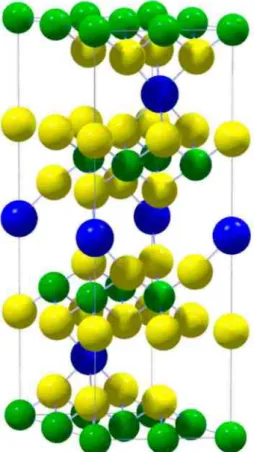
The final structure is represented in Fig. 2. Due to the limited computational resources that impose a moderately
35 30 25 20 15 10 5 0
-4 -3 -2
E - EF (eV)
-3 -2 -1
E - E F (eV)
FIG. 1. (Color online) Comparison of DOS for two Na3Ti3S6 compounds (one based on the la-NaxTiS2 phase and another based on the lb-NaxTiS2 phase) and for a host Ti3S6 compound.
large unit cell, we have to limit the size of the intercalated compound cell to Na3Ti1 2S2 4, i.e., x = 0 . 2 5 , higher than 0.1 but within a low intercalation range.
III. METHOD
The scheme followed in this study was introduced as a simplified version of the rotational invariant formulation of the G G A + U method (Ref. 16 and references therein). In this formulation an extra EU component is introduced for total
energy which depends on the occupation coefficients of the
considered strongly correlated statesD J mm nJ ,' J and it is tuned by
the term U,
Eu\nZm,] = 2 2 T r[ n' > ( 1 - ni j) ]. (1)
2 i, j
In the equation above ni,<J is the total summation of
occupa-tions over all the strong correlated states of site i and spin J. The occupation matrix coefficients are calculated as
= 2 f J M k, v
k,vl Pmm (2)
where J J v is the electronic wave function of the v state in k
with spin J, f Jv is the corresponding occupation number, and Pimm , are the projection operators, which in our case
corre-! l J l '
spond to Wannier functions.2 3
U is assigned to the value of the spurious curvature of the total energy of the system with respect to the variation in the number of electrons. It can be obtained following a linear-response method from constrained D F T calculations in which a small potential shift is applied to the correlated
FIG. 2. (Color online) Structure of the modeled Na3Ti12S24 compound. S, Ti, and Na atoms are filled in yellow (light gray), green (medium gray), and navy blue (dark gray), respectively.
states. If a potential shift a , is applied to the atom , , the response function in the atom i is defined as
Xij
da,
and the value of U corresponds to the diagonal term
U = ( X -1- X"1);;.
(3)
(4) The response matrix x0 refers to the bare perturbation without allowing the redistribution of the whole electronic system toward the self-consistency, while X refers to the self-consistent response function. In order to approach the full magnitude of the response function, it is necessary to per-form calculations in unit cells as large as possible.
Plane-wave-based QUANTUM-ESPRESSO code2 4 was used
for the calculations with ultrasoft pseudopotentials.2 5 The
Na3Ti1 2S2 4 whole atomic structure was allowed to be relaxed below the convergence thresholds of 0.4 mRy/bohr for the atomic forces and 0.5 kbar for the pressure. The PW91 functional2 6 was selected to parametrize the
exchange-correlation potential of the G G A calculations. A Methfessel-Paxton first-order technique2 7 with 5 mRy of smearing was
used to obtain the occupation of one-particle levels in the Brillouin zone, whose sampling was 7 X 7 X 13 and 6 X 6 X 2 for the 3 X 3 X 1 supercell of TiS2 and the unit cell of Na3T1 2S2 4, respectively. The DOSs were calculated follow-ing the tetrahedron method.2 8 Wannier-type projectors used
0.013
0.012
0.011
| 0.01
•Se 0.009
TiL (S-C) — i
-Ti1STN(S-C)
--X--Ti2ND n.(S-C)
TiL (B)
EJ-T i^N . B )
----••-^N D N (B) - - & • •
(eV)
FIG. 3. (Color online) Occupation of localized levels of the different Ti; atoms of TiS2 compound with respect to a, potential shifts, both allowing the relaxation to the self-consistency (S-C) and not (B) for constructing X and X0, respectively. The TiL label cor-responds to the same atom in which a, is applied. Ti1sW is referred to the six first Ti neighbors and Ti2ndiv corresponds to the two sec-ond neighbors of TiL.
in the G G A + U scheme to obtain the highly localized occu-pations were created by a postprocessing routine included in the QUANTUM-ESPRESSO package from converged Kohn-Sham states obtained in previous GGA calculations.
IV. RESULTS
A. TiS2
In the first stage the electronic valence-band structure for bulk TiS2 was calculated. A 3 X 3 X 1 supercell of TiS2 was selected in order to calculate U following the scheme ex-plained above. The use of this cell includes not only the contribution from the nearest Ti neighbors which are placed at 3.41 A but also that one from the second-nearest neigh-bors located at 4.82 A.
As can be seen from Fig. 3, in order to obtain the response functions X and Xo the potential shifts employed on this oc-casion were not centered on zero, as is usual in the scheme of Ref. 16, but in - 0 . 2 eV. The reason is that the 3d levels in the TiS2 compounds are essentially empty, and therefore the additional discouragement which would be usually achieved by a positive potential shift applied is not originated prop-erly. In these circumstances the use of small negative poten-tial shifts allows this kind of difficulties to be overcome. Their use is guaranteed because the resulting occupations are above zero but almost negligible (always below 0.015 elec-tron per Ti atom). A stable behavior of U at 2.1 eV has been checked when applying potential shifts around - 0 . 2 eV.
Having obtained the value of 2.1 eV for U a G G A + U
calculation was carried out. The resulting G G A + U DOS is shown against that obtained with GGA in Fig. 4. It can be seen that the use of the computed U has brought about a band gap of 1 eV between the S 3p and the Ti 3d bands, while in the GGA result this gap is not present.
SANCHEZ, PALACIOS, AND WAHNON PHYSICAL REVIEW B 78, 235121 (2008)
- 3 - 2 -1 E - Ef (eV)
FIG. 4. (Color online) Total DOS for Ti9S18 compound calcu-lated with GGA and GGA+ U scheme using an ab initio value for U
of 2.1 eV.
method. First a Lorentzian convolution was made which simulates the finite lifetime of the excited electrons and whose full width at half maximum (FWHM) is linearly pro-portional with a coefficient 0.1 to the binding energy of the valence electrons.29 Afterward there was applied a Gaussian
convolution with a constant F W H M which in this case rep-resents the spectrometer resolution—in this case 63 meV. Finally a background proportional to the integrated intensity of lower binding energies was added following a Shirley-type method.3 0 The spectrum obtained is presented together
with the experimental HeI-UPS results3 in Fig. 5.
From Fig. 5 it can be seen that the locations of the three main peaks of the S 3p band in both spectra agree. The only feature that is not completely reproduced is the relative size of the peaks. However, it must be taken into account that UPS is essentially a surface technique, and therefore the crystal orientation is an important factor which can modify the peak intensities. Furthermore, background addition method could be improved by using a more refined method, but the differences due to this fact are not expected to be significant.
8 0 0 1 1 1 1 1—
G G A + U U = 2 . 1 e V
7 0 0 JW U P S E x p
-7 0 0 U P S E x p
-/
6 0 0 /
/
\y \ni
5 0 0 / /
•e •S
y 4 0 0 s \\ \ •
w
n 3 0 0
Hz v.,
2 0 0
100
0
10 6 4 2
Binding E n e r g y (eV)
FIG. 5. (Color online) Photoemission spectra of ^S1 8 com-pound obtained with GGA+ U (U =2.1 eV) compared to UPS spec-trum (HeI) from Ref. 3.
(a)
J i a ' L C S C ) 0 . 3 4
0 . 3 2
T i a1s tN( S - C ) —
-X--T ib 1s tN( S - C ) *
T i b 2n dN ( S - C ) E H
TiaL(B) • -Tia 1stN (B) ••••©••
Tib 1stN (B)
---Tib2ndN(B) - " A "
M
0 . 3 4
(b)
Tib L (S-C) ^ 1
-Tib 1stN (S-C) X
-Tia 1 stN (S-C) *
Tia2ndN(S-C) E H .T i b L ( B ) 0 . 3 2 • Tjb 1st N(B)
Tia 1stN (B) •••••••
Tia2ndN(B)
£2 0.28
0.26
0 . 2 4
0 . 2 2
-0.05 -0.02 0 0 . 0 2 0.05 - 0 . 0 5 -0.02 0 0 . 0 2 0.05
FIG. 6. (Color online) Occupation of localized levels of the different Tii atoms for Na3Ti12S24 compound with respect to applied a j potential shifts [over sites Tia and Tib for (a) and (b), respec-tively]. The labels have the same meaning as in Fig. 3, except that Tia and Tib are considered as independent species, and therefore local and neighbor sites noted here have been split into a and b
types.
B. Na^TiS2
In this part of the work the electronic structure of Na3Ti1 2S2 4 is calculated following a method analogous to that explained above, and thus the first step needed to be fulfilled is again the obtaining of the corresponding Hubbard term. In principle we suppose that the influence of the inter-calated Na should not be important for the determination of
U because Na atoms are located intentionally in a highly homogeneous arrangement. However in the compound shown in Fig. 2 not all the twelve Ti atoms are completely equivalent, but there are three of them (one per layer) which are surrounded by six first Na neighbors equidistant to them. From now on these Ti atoms will be labeled as Tia. The other nine (Tib) are surrounded by some Na atoms closer than others. This small difference is reflected in the localized oc-cupations being 0.29 and 0.24 electrons for Tia and Tib, re-spectively. It is noted that if the twelve Ti were equivalent all the local occupations would be 0.25 electrons.
Therefore, a study taking these two Ti sites as indepen-dent atomic species was carried out for the calculation of U.
The resulting occupations obtained for the localized states and for the different potential shifts applied are shown in Fig.
6. The results of the on-site screened correlation term turned out to be UTi =2.62 eV and UT^ = 2 . 6 0 eV, which implies that all the Ti atoms can be considered as equivalent.
Consequently, the DOS at G G A + U level for Na3Ti1 2S2 4 was calculated using a unique value of U =2.6 eV for the twelve Ti atoms. In Fig. 7 this DOS is shown with another
aj (eV) aj (eV)
E - Ef (eV)
FIG. 7. (Color online) Total DOS for Na3Ti12S24 compound calculated with GGA and GGA+ U using an ab initio value for U of 2.6 eV.
one calculated following the GGA scheme. It can be seen that a band gap of 1.2 eV appears for the G G A + U results, while in the GGA standard DOS there is no appreciable gap. Finally, postprocess tasks analogous to those introduced above were performed in order to compare the G G A + U re-sults with the available experimental UPS spectra (see Fig.
8), including again Lorentzian and Gaussian broadenings and Shirley-type background addition. There is resemblance be-tween both spectra, and the main peaks binding energies are close to the experimental ones. However there are few fea-tures that are different in them. On one hand, and as hap-pened to the TiS2 case, the sizes of the different S 3p peaks disagree and the explanation proposed is the same as that explained above. On the other hand a small new peak ap-pears with binding energy at about 8 eV. This peak is as-signed in Ref. 4 to a slightly different hybridization of S atoms caused probably for some disorder in the slab stack-ing.
Nevertheless, calculated spectra of Fig. 8 have been shown to reproduce a band gap between S 3p and Ti 3d
bands that agrees to a large extent with the experimental
FIG. 8. (Color online) Photoemission spectra of Na3Ti12S24 compound obtained with GGA+ U (U =2.6 eV) compared to UPS spectrum (HeI) from Ref. 3.
measurements, unlike GGA, which was not able to predict a significant band gap in the Na-intercalated TiS2.
V. SUMMARY AND CONCLUSIONS
In the present work an ab initio G G A + U study has been applied in order to obtain the valence electronic structure of TiS2 compounds, both bulk and Na intercalated with a com-position approximate to N a0 1T i S2. A Na3Ti1 2S2 4 unit cell was modeled for carrying out the G G A + U study for the intercalated material. It is argued that the only important fac-tor that affects the valence electronic structure of NaxTiS2 compounds is the quantity of intercalated Na, while the ge-ometry of its site and the stacking of the TiS2 layers are largely irrelevant.
Following the method set out by Cococcioni and de Gironcoli1 6 the on-site correlation term U of Ti 3d electrons
of Ti9S18 compound has been calculated as 2.1 eV. In the case of Na3Ti1 2S2 4, even though there is slightly inhomoge-neous arrangement of the surrounding Na atoms, the ob-tained result of U was 2.6 eV for all of the Ti atoms consid-ered as equivalent.
The difference found between the values of the strength of the Hubbard term in both compounds is attributed to the different valence states of the Ti atoms. In the case of TiS2 all of the Ti atoms have a valence of 4+, while in the inter-calated compound the additional charge provided by the Na 3s electrons is transferred to the Ti 3d levels resulting in a valence state close to Ti3 . 7 5 +.
This increase in the obtained Hubbard term is reflected in the subsequent G G A + U calculations carried out with the corresponding U values, showing band gaps of 1 and 1.2 eV for both bulk and Na-intercalated TiS2, respectively. Those band gaps are originated by means of the enhancement of the single-particle energies of the Ti 3d electronic levels with respect to the other states. Standard GGA calculations did not produce a significant band gap in any of the compounds studied.
A postprocess work for calculated DOS has been carried out in order to compare the results with available UPS ex-perimental data. The S 3p binding energies are close to those of the UPS measurements. Discrepancies in some relative intensities of the different peaks which make up the S 3p
band can result from the influence of the sample orientation. In the case of the Na3Ti1 2S2 4 calculations, they do not show a small experimental peak at 8 eV, but its origin seems to come from perturbations in the slab stacking.4
SANCHEZ, PALACIOS, AND WAHNON PHYSICAL REVIEW B 78, 235121 (2008)
ACKNOWLEDGMENTS
The authors would like to thank J. C. Conesa for fruitful discussions at the origin of this work and D. Tonti for sharing experimental results and data. They also would like to
ac-knowledge funding from the C A L I B A N D Project of the Spanish Ministry of Education and Science (Grant No. MAT2006-10618). They thankfully acknowledge the com-puter resources and assistance provided by the Centro de Supercomputacion y Visualization de Madrid (CeSViMa).
1M. Broussely, P. Biensan, and B. Simon, Electrochim. Acta 45, 3 (1999).
2 J. Dijkstra, C. F. van Bruggen, and C. Haas, J. Phys.: Condens. Matter 1, 4297 (1989).
3 D. Tonti, C. Pettenkofer, and W. Jaegermann, Electrochem. Solid-State Lett. 3, 220 (2000).
4D. Tonti, Ph.D. thesis, Freie Universitat Berlin, 2000 (http:// www.diss.fu-berlin.de/2000/145/).
5F. R. Shepherd and P. M. Williams, J. Phys. C 7, 4416 (1974). 6 C. A. Kukkonen, W. J. Kaiser, E. M. Logothetis, B. J.
Blumen-stock, P. A. Schroeder, S. P. Faile, R. Colella, and J. Gambold, Phys. Rev. B 24, 1691 (1981).
7 C. H. Chen, W. Fabian, F. C. Brown, K. C. Woo, B. Davies, B. DeLong, and A. H. Thompson, Phys. Rev. B 21, 615 (1980). 8P. C. Klipstein and R. H. Friend, J. Phys. C 17, 2713 (1984). 9C. M. Fang, R. A. de Groot, and C. Haas, Phys. Rev. B 56, 4455
(1997).
1 0D. R. Allan, A. A. Kelsey, S. J. Clark, R. J. Angel, and G. J. Ackland, Phys. Rev. B 57, 5106 (1998).
11S. Sharma, T. Nautiyal, G. S. Singh, S. Auluck, P. Blaha, and C. Ambrosch-Draxl, Phys. Rev. B 59, 14833 (1999).
12A. H. Reshak and S. Auluck, Phys. Rev. B 68, 245113 (2003). 13P. Hohenberg and W. Kohn, Phys. Rev. 136, B864 (1964). 14W. Kohn and L. J. Sham, Phys. Rev. 140, A1133 (1965). 15 V. I. Anisimov, J. Zaanen, and O. K. Andersen, Phys. Rev. B 44,
943 (1991).
16M. Cococcioni and S. de Gironcoli, Phys. Rev. B 71, 035105 (2005).
17 Q. Yan-Bin, Z. Guo-Hua, L. Di, W. Jiang-Long, Q. Xiao-Ying, and Z. Zhi, Chin. Phys. Lett. 24, 1050 (2007).
18J. J. Yeh and I. Lindau, At. Data Nucl. Data Tables 32, 1 (1985). 19D. A. Shirley, Phys. Rev. B 5, 4709 (1972).
20R. Kwok, http://www.phy.cuhk.edu.hk/~surface/XPSPEAK. 21 H. J. M. Bouwmeester, E. J. P. Dekker, K. D. Bronsema, R. J.
Haange, and G. A. Wiegers, Rev. Chim. Miner. 19, 333 (1982). 22 K. Cenzual, L. M. Gelato, M. Penzo, and E. Parthe, Acta
Crys-tallogr. B 47, 433 (1991).
23G. H. Wannier, Phys. Rev. 52, 191 (1937).
24P. Giannozzi et al., http://www.quantum-espresso.org 25D. Vanderbilt, Phys. Rev. B 41, 7892 (1990).
26J. P. Perdew, J. A. Chevary, S. H. Vosko, K. A. Jackson, M. R. Pederson, D. J. Singh, and C. Fiolhais, Phys. Rev. B 46, 6671 (1992); 48, 4978 (1993).
2 7M. Methfessel and A. T. Paxton, Phys. Rev. B 40, 3616 (1989). 28P. E. Blochl, O. Jepsen, and O. K. Andersen, Phys. Rev. B 49,
16223 (1994).
29 H. Hochst, P. Steiner, G. Reiter, and S. Hufner, Z. Phys. B Con-dens. Matter 42, 199 (1981).