I m p l i c a t i o n s of l o w b r e a k d o w n v o l t a g e of c o m p o n e n t
subcells on external q u a n t u m efficiency m e a s u r e m e n t s
of m u l t i j u n c t i o n solar cells
Enrique Barrigón , Pilar Espinet-González, Yedileth Contreras and Ignacio Rey-Stolle
ABSTRACT
The electrical and optical coupling between subcells in a multijunction solar cell affects its external quantum efficiency (EQE) measurement. In this study, we show how a low breakdown voltage of a component subcell impacts the EQE deter-mination of a multijunction solar cell and demands the use of a finely adjusted external voltage bias. The optimum voltage bias for the EQE measurement of a Ge subcell in two different GalnP/GalnAs/Ge triple-junction solar cells is determined both by sweeping the external voltage bias and by tracing the I-V curve under the same light bias conditions applied dur-ing the EQE measurement. It is shown that the I-V curve gives rapid and valuable information about the adequate light and voltage bias needed, and also helps to detect problems associated with non-ideal I-V curves that might affect the EQE measurement. The results also show that, if a non-optimum voltage bias is applied, a measurement artifact can result. Only when the problems associated with a non-ideal I-V curve and/or a low breakdown voltage have been discarded, the mea-surement artifacts, if any, can be attributed to other effects such as luminescent coupling between subcells. Copyright © 2015 John Wiley & Sons, Ltd.
KEYWORDS
Ge subcell; breakdown voltage; external quantum efficiency; multijunction solar cells
1. INTRODUCTION
III-V-based multijunction solar cells (MJSCs) consist of a series connection of different subcells and show nowadays the highest conversion efficiencies for any photovoltaic device. For instance, the most widespread, commercially available, MJSC is a triple-junction solar cell (3JSC) formed by a GalnP-based top cell (TC) of ~1.9eV, a GalnAs-based middle cell (MC) of ~1.4eV and a Ge bottom cell (BC) of ~0.6eV grown on Ge substrates. In recent years, several 3JSC designs such as metamor-phic [1], inverted metamormetamor-phic [2], architectures based on dilute nitrides [3] or 3JSCs using bifacial epigrowth [4] have achieved efficiencies higher than 40% by the use of BCs close to 1 eV. MJSC with four junctions have achieved even higher efficiencies by the mechani-cal bonding of two dual-junction solar cells [5], and in the near future, current 3JSC are expected to achieve
higher efficiencies by adding a low-bandgap fourth junc-tion such as a Ge subcell. The characterizajunc-tion of the electrical and optical properties of each subcell used in such structures is a challenging task, since the subcells in an MJSC are not accessible independently—MJSC are generally two-terminal devices—and the electro-optical coupling between subcells in a MJSC stack has to be taken into account.
wavelengths corresponding to another subcell. The origin of the so-called measurement artifact has been thoroughly discussed in recent years and has been related to a variety of causes such as a low shunt resistance in any junction [8,9], luminescent coupling [10-12] or a combination of both [13]. In brief, these papers show that the EQE of a subcell is not only determined by its own properties but also by the electro-optical interactions with other sub-cells in the stack. Light and voltage bias (Vj,¡aj) conditions
have been suggested to minimize or eliminate this artifact [8,14,15], and a procedure has been already established to obtain the real EQE out of a device with strong luminescent coupling [12,15,16].
So far, only the implications of a component subcell with a low shunt resistance and luminescent coupling between subcells on the EQE determination have been thoroughly studied. However, little attention [6] has been given to the impact of low breakdown voltage (V¡,r) of a component subcell—characteristic of low bandgap solar cells—on its EQE measurement. In this paper, we com-plete the vision of the EQE measurement of MJSCs. We analyze the influence of a low V¡,r of the Ge subcell on the determination of the proper voltage and light bias con-ditions necessary to measure the EQE of this device in a complete GalnP/GalnAs/Ge 3JSC. If an erroneous V^(as is applied, a similar measurement artifact as described ear-lier appears, but with a completely different origin. As it will be shown later, in order to unequivocally determine the origin of the measurement artifact in the EQE spec-tra, it is important to first discard, among others, a low
V¡,r in a subcell as the origin of the measurement artifact. Besides, we show how the I-V curve of the MJSC— measured under the same light bias conditions applied for the EQE measurement—helps not only to quantify the required V¡,ias but also to detect non-ideal I-V curve prob-lems (such as shunt resistance) or even if the light bias applied is adequate. The observations described in this paper for a GalnP/GalnAs/Ge 3JSC are directly applicable to the characterization of any MJSC with a low bandgap component subcell.
2. EXPERIMENTAL
2 . 1 . EQE measurement
The setup used for the EQE measurements consists of a Xe lamp used as white light source which passes through a Horiba Jobin Yvon monochromator (TRIAX180) and a filter wheel. The monochromatic light is chopped at a fre-quency of 481 Hz and optically guided to the device under test and to a monitor cell. Two different low noise cur-rent preamplifiers (SR570) convert the output curcur-rents into voltages, which are measured by a two-channel lock-in amplifier (Anfatec 203). The monitor cell is always mea-sured and corrects the lamp fluctuations that may take place during the measurement. A set of lasers (632.8 nm
and 806 nm) and a halogen lamp with different opti-cal filters constitute the multi-source spectrally tunable light bias used along the study. The low noise current preamplifier is also used to voltage bias the device under test. Throughout the text, voltages are defined as posi-tive numbers by convention, whereas the sign indicates the quadrant or is as a result of an algebraic manipulation. I-V curves were measured with a source-meter instrument Keithley 2602.
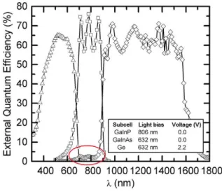
Due to the series connection of the subcells in a mono-lithic MJSC configuration, special techniques have been developed to measure the EQE of any subcell in the stack [17]. Reviews on this procedure can be found elsewhere [8,18]. In summary, the EQE is derived from the current extracted from the device at a given wavelength under a given light bias. As a result, the EQE measured will cor-respond to the subcell generating the lowest photocurrent, namely, the current-limiting subcell. The EQE measure-ment of a particular subcell in a monolithic MJSC stack requires accordingly sub-illuminating the subcell of inter-est (in respect to the other subcells in the stack) so that it generates the appropriate one-sun photocurrent. Through-out the text, the expression "X-limiting light bias" will be employed to refer to the aforementioned special combina-tion of light sources needed for the EQE measurement of the X subcell, where X is the TC, MC or BC. Additionally, to achieve short circuit conditions on the subcell of inter-est, a V¡,ias equal to the sum of the Voc of the non-limiting subcells should be applied to the MJSC [8]. Nonetheless, this is not necessary for a subcell with an I-V curve that shows a flat slope around short circuit conditions. Hence, the spectral content and intensity of the light bias together with the value of V¡,ias have to be carefully determined for the measurement of the EQE of an MJSC. For instance, Figure 1 shows the EQE spectra of the GalnP, GalnAs and
400 600 800 10001200140016001800
X (nm)
Figure 1. External quantum efficiency measurement of a GalnR
GalnAs and Ge component subcells of a 3JSC. In the inset, the light and voltage biasing conditions are shown. The red circle
Ge subcells of a 3JSC with no antireflection coating. The light and voltage bias settings (see inset of Figure 1) were empirically determined in order to maximize the EQE of each subcell.
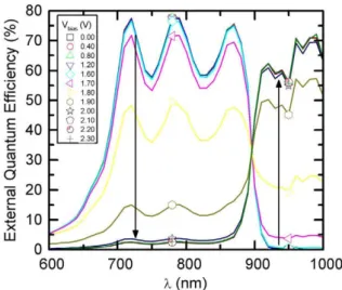
As mentioned earlier, we are particularly interested in the measurement conditions of the Ge subcell in an MJSC stack. For the measurement shown in Figure 1, a V\,ias °f 2.20 V must be applied, which corresponds approximately to the sum of the Voc of the TC and MC. As shown in Figure 1, with these biasing conditions, the EQE curve of the BC still exhibits some response in the MC spec-tral range (i.e., a measurement artifact) between 700 and 850 nm. The measurement artifact is marked with a circle in Figure 1. In order to check for shunt resistance problems that could be affecting the EQE measurement, we decided to sweep the V¡,ias applied to the 3JSC. Figure 2 shows the Ge EQE measurements for the same cell used in Figure 1 under variable V¡,¡as, while the light bias on all the subcells is kept unchanged. For clarity, the EQE of the Ge subcell is only shown until 1000 nm in this figure. If a Vuas lower than 2.10 V is applied (see for example the EQE spectrum in Figure 2 for Vbias = 1.90 V), the EQE of the BC starts to decrease, while the response in wavelengths characteris-tic of the MC increases. Hence, the measurement obtained shows an even higher measurement artifact as described before. As long as we reduce the external V¡,¡as, the EQE of the MC steadily increases whereas the EQE of the BC decreases until a V¡,ias of 1.80 V is applied, where the EQE of the MC is even higher than that of the BC. Indeed, the EQE measured for V\,ias — 1-60V entirely corresponds to the MC, being the EQE of the BC zero. While the measurement of the MC instead of the BC could be also interpreted as a measurement artifact, we restrict the use of this term for the cases where two different subcells are simultaneously measured.
600 700 800 900 1000 X (nm)
Figure 2. External quantum efficiency measurements with the
light bias settings to measure the Ge subcell under different external voltage bias. Arrows indicate the tendency of the EQEs
as the external applied voltage bias to the 3JSC increases.
In other words, despite the BC-limiting light bias is being used, there is only a narrow V\,ias range (2.10 to 2.30 V in this experiment) where the BC can actually be measured, and not even perfectly because a minimum response is still present in the MC spectral range. Moving
Vbias °ut of this range, either up or down, changes the EQE
measured to a composed curve with contributions of the MC and BC to the EQE.
At first glance, this effect could be attributed to the presence of a low shunt resistance in the Ge BC. How-ever, this does not provide a satisfactory explanation for a number of reasons, because (1) there is a Villas range where a constant EQE of the Ge BC is measured, (2) there is a Vbias range where measurement artifacts appear (both in the MC and the BC) which are independent of the light bias applied to the MC and TC and (3) the EQE of the MC is correctly measured for V¡,ias < 1.6V despite the BC-limiting light bias condition. Luminescent cou-pling effects at high Vuas between MC and BC are also discarded as an explanation for the tendency observed in Figure 2, because the operating point of the MC (close to its Voc) does not significantly change with V¡,ias while measuring the BC [19]. Consequently, the amount of radia-tive recombination that takes place in the MC (i.e., the number of photons potentially absorbable by the BC) remains unaltered with varying V¡,¡as. Besides, lumines-cent coupling will not explain why the EQE of the MC appears for low V¡,ias. Hence, we propose another origin for the tendency observed in Figure 2, namely, low break-down voltage of the Ge BC. We will show that in some cases, the effect of a low v£, (breakdown voltage of the BC) affects not only the EQE measurement of the BC but also it can be erroneously identified with luminescent coupling effects.
2.2. Samples under s t u d y
For this study, GalnP/GalnAs/Ge 3JSC structures were grown and processed into solar cells. The 3JSC consists of a 675nm-thick 1.8 eV GalnP-based TC, a 3 |xm-thick 1.4 eV GalnAs-based MC and 0.6 eV Ge BC. The Ge junc-tion is formed by diffusion of group V elements in the p-type Ge wafer during growth. No antireflection coating was deposited on the cells. For details on the Metalor-ganic Vapor Phase Epitaxy (MOVPE) growth of the 3JSC structures, the reader is referred elsewhere [20].
According to the characteristics of the Ge subcell, the origin of the breakdown voltage can be avalanche, tunnel-ing (i.e., Zener) or a combination of both. The dominant mechanism is avalanche for the doping levels of these samples, although tunneling cannot be neglected. Indeed, we are able to modify the breakdown voltage with the doping level of the base of the Ge subcell, since V¡,r is approximately described by the following expression [21]:
where N¿ and A^ are the acceptor and donor impurity concentration for the p-region and n-region, respectively. For 3JSC grown in MOVPE ambient, the doping level of the emitter (around 1.1 x 10 cm ) is much higher than the doping level of the base. Therefore, Equation 1 can be derived to the following:
Vbr a 1 (2)
Accordingly, in order to study the effect of the break-down voltage on the EQE measurement of the Ge sub-cell, two different substrates with different doping lev-els were used to grow the 3JSC structures, namely 4 x 10¹⁷ and 1 x 1018 cm . As it will be shown later, in
this way, the reverse characteristic of the Ge subcell is accordingly modified.
600 700 800
X(nm)
900 1000
Figure 3. External quantum efficiency measurements of a 3JSC
under BC-limiting light bias and under different voltage bias for a BC with high (a) and low (b) breakdown voltages. For clarity, the external quantum efficiency measurement of the Ge BC is
only shown until 1000 nm.
3. RESULTS
3 . 1 . EQE measurement o f Ge subcells in 3JSC
In order to clarify the role of Vr in the EQE measure-ment, we first analyze the voltage bias needed to measure the EQE of a Ge BC in a 3JSC with a relatively high V¡,r (i.e., base doping level of 4x10 cm ). Subsequently, we analyze the V\,ias needed for a Ge BC with a lower V¡,r (i.e., base doping level of 1 x 10 cm ) and finally compare these two cases. In Figures 3-5, the sample with higher
BC BC .
and the sample with lower Vr will be identified by red circles and black squares, respectively.
As shown with filled red circles in Figure 3(a), the EQE measured at short circuit conditions (V¡,¡as = 0 V) corresponds to the MC, despite having over-illuminated the TC and MC subcells. As a matter of fact for this 3JSC, this situation holds until a voltage of 0.50 V is applied, where the EQE of the MC initiates a slight decrease, while the EQE of the BC starts to appear. Figure 4 synthesizes this evolution versus voltage. For clarity, only the EQE at 750 nm (i.e., wavelength where only the MC should show response) and at 950 nm (i.e., wavelength where only the BC should show response) versus V¿¿aj are represented in
Figure 4. These two wavelengths are indicated with dashed vertical lines in Figure 3. According to the evolution of the EQE with V¡,¡as, we identify in Figure 4 three differ-ent voltage regions. Region I indicates the voltage region where the MC is measured. As shown in Figure 4(a), from 0.50 V on the EQE of the MC decreases while the EQE of the BC increases (identified as Region II). This Region II will be also called hereafter the artifact region, because in this voltage range, the measurement artifact takes place. Region II continues until we reach 1.29 V, where the EQE at 750 nm (i.e., of the MC) reaches a constant value close to zero and the EQE at 950 nm (i.e., of the BC) maxi-mizes (Region III). As shown in Figure 4(a), this maximum EQE at 950 nm or, in other words, the EQE of the Ge sub-cell does not change with V\,ias until a V\,ias °f 2.29 V is applied. Figure 3(a) confirms this fact because it shows that the measurements of the Ge subcell taken at 1.40 V (red stars) and 2.20 V (open red circles) are identical (for clar-ity reasons, the EQE of the Ge subcell is only shown until 1000 nm in this figure). Vertical dashed lines in Figure 4 correspond to the V\,ias applied for the complete EQE measurements represented in Figure 3, namely 0, 1.40 and 2.20 V
For the 3JSC with a Ge BC with lower V¡,r (i.e., higher base doping level), we also measure the MC response if no
V\,ias is applied (see filled black squares in Figure 3(b)).
As contrary as observed for the other sample, if we apply a Vbias of 1.40 V, we still measure the EQE of the MC (see how open black stars overlap filled squares in Figure 3(b)). Figure 4(b) shows the EQE at 750 and 950 nm for this 3JSC versus V¿¿aj. In this case, Region II begins at a V¿¿aj
B
c
m
o i t
LU
E 13 - i — '
C ro
13 O ro c
X LU
B
c gj
o
i t UJ
E 13
-i—<
C ro
13 O ro c
X UJ
70
60
50
40
30
20
10
0 70
60
50
40
30
20
10
0 Ü
BC with high Vbr
—•— EQE @ 750 nm EQE @ 950 nm
R e g i o n I
BC with low V
E Q E @ 7 5 0 n m E Q E @ 9 5 0 n m
_L
200
0 500 1000 1500 2000 2500
V b ia s (m V)
Figure 4. External quantum efficiency measurements at
750 nm (filled symbols) and at 950 nm (open symbols) for a Ge component cell with high (a) and low (b) breakdown volt-ages. Lines are set as a guide to the eye. AV represents the voltage Interval where the measurement artifact takes place
(I.e., Region II).
the Ge BC is maximized if a V\,ias higher than 2.09 V is applied (Region III), whereas the EQE value of the MC becomes constant and close to zero. In this case, Region III (i.e., the voltage interval of V\,ias where the Ge sub-cell response is accurately measured) is only of about 0.20 V, meanwhile, in the 3JSC with higher, V?c was of
' ' © ' fry
almost 1.00 V. Open black squares in Figure 3(b) corre-spond to the EQE of this BC at 2.20 V. Finally, it has to be pointed out that the EQE value of the MC obtained at 750 nm and the EQE of the BC at 950 nm in Figure 4(b) are now lower and higher than in Figure 4(a), respectively, because the positions of the maxima and the minima in the EQE are different in both cells, as can be seen with the vertical dashed lines at 750 and 950 nm in Figure 3 (note that the devices do not have an antireflection coating). In summary, the minimum V¡,ias and in turn the voltage
150 =.
1.100
50 -ü
-50
- i — | — i — | — i — | — i — | 1—|—r gion I Region II Region III
^
v
AV V°
;+ v=cc V / ^
BC with high Vt
BC with low V
J i L
/ • _ l i
-0.5 0.0 0.5 1.0 1.5 2.0 2.5 Voltage (V)
Figure 5. I-V curve of the 3JSCs under the same light bias
conditions applied during the external quantum efficiency mea-surements (I.e., TC and MC overlllumlnated). Red circles and black squares correspond to the 3JSC that BC presents a high
and a low breakdown voltage, respectively.
interval where the BC can be measured (i.e., Region III) seem to be directly linked to the breakdown properties of the Ge subcell.
3.2. I-V curves of the 3JSC under the light bias used during the EQE measurement
Because the measurement of the EQE is directly linked to the current extracted from the device, we measured the I-V curve (Figure 5) of each 3JSC under the same exter-nal light bias conditions that were applied for the EQE results in Figures 3 and 4. The shape of the I-V curves is the one expected as described in [6] for a 3JSC with a relatively low Vr under BC-limiting light bias condi-tions. The I-V curves also present three different regions, identified in Figure 5, only for the BC with high V¡,r. At short circuit conditions, the current-limiting subcell in both 3JSCs is the MC although the Ge subcell photogen-erates less current than the MC, as can be observed in Region III of the figure. The MC, and not the TC, was identified as the current-limiting subcell because its EQE was measured under these light and voltage biasing con-ditions (Figure 4). In both I-V curves, as the voltage is increased, the 3JSC enters in a transition region from the MC to the BC limited area (Region II), which corresponds to the artifact region described in Figure 4. The slope and the shoulder close to the BC limiting area approximately reproduce the shape of the reverse I-V curve of the Ge subcell. Once enough V¡,ias is applied (Region III), the constant current level measured corresponds to the Ge sub-cell, because under these conditions, the EQE of the BC is recorded. For the 3JSC with a relatively high Vr (i.e., base doping level of 4x10 cm ), Region II starts at a 0.459 V and ends at 1.389 V For the 3JSC with lower V?c
br
4. DISCUSSION
4 . 1 . Operating point of the subcells during the EQE measurement
During the EQE measurement, the operating point of each individual subcell is determined by the requirement of cur-rent continuity through the device, together with the fact that the MJSC is kept at a given voltage bias. Let us con-sider the EQE measurement of an ideal MJSC (i.e., neither showing a low shunt resistance nor a low breakdown volt-age in any subcell) kept at a voltvolt-age bias of zero volts and at a given light bias to under-illuminate one of the subcells. In this situation, the non-limiting subcells oper-ate at a voltage close to their Voc (being the exact value determined by the current of the under-illuminated sub-cell) while the current-limiting subcell operates in reverse bias at approximately a voltage equal to the sum of the Voc
c ^, T , n / x-^ T riion-limiting SC\ ^
of the non-limiting subcells I - 2_, Voc ) • ™r instance, during the EQE measurement of the Ge subcell in a GalnP/GalnAs/Ge 3JSC (for Vbias=0V), the BC works
at"(Voc + Voc ) (i-e->r e v e r s e biased) whereas the TC and
MC work at a voltage close to their respective Voc as deter-mined by the current of the BC. Please notice that the Voc here are defined under the illumination needed for the EQE measurement and not under standard test conditions.
However, if one of the subcells of the MJSC shows a relatively low breakdown voltage (e.g., the Ge BC), the situation just described, in terms of subcell operating volt-ages, changes significantly. We will analyze this situation with the aid of Figure 6. This figure shows with a dashed black line the I-V curve of a GalnP/GalnAs/Ge 3JSC that would be obtained when illuminating the solar cell with the light bias used for the EQE measurement of the Ge BC (i.e., a BC-limiting light bias). In this figure, the I-V curves of all the subcells have also been included to assess the operating voltage of each subcell. Since the I-V curve of the Ge subcell (red line) shows a low V¡,r, the I-V curve of the 3JSC presents a similar shape as the experimental I-V curve of Figure 5 under such light bias. As explained above, if the 3 JSC is kept at short circuit conditions, the Ge subcell should operate in reverse bias at approximately the sum of the Voc of TC and MC. However, since the break-down voltage of the Ge subcell is lower than V^r + V¿* , the MC shows up in this particular case as the new current limiting subcell, even though the light bias used produces less photocurrent in the BC. Please note, that the term "current limiting" here is not only linked to photogenera-tion but considers both photogeneraphotogenera-tion -that depends on illumination- and breakdown -that depends on voltage bias. Under these conditions, the TC operates at a point close to its Voc (labeled Vi in Figure 6) and the BC works in the breakdown region (labeled V? in Figure 6). For both subcells, the operating voltage is determined by the photo-current of the MC. Accordingly, the MC operates in reverse bias, at approximately the Voc of the TC minus the
<D .
O
BC MC TC U V0c V0c «oc
Voltage (a.u.)
Figure 6. Schematic subcell I-V curves of a GalnP/GalnAs/Ge
(blue, green and red lines, respectively) triple-junction solar cell under BC-limiting light bias in which the low Vbr of the Ge sub-cell is taken into account. The black dashed line represents the composite I-V curve of the 3JSC. Currents and voltages with subscript 1 represent the operating point of the subcells when the MJSC is kept at short circuit (black circle). The green dashed line represents the I-V curve of the MC when a monochro-matic excitation is superimposed to the light bias. The operating points of the subcells under the effects of monochromatic light
are indicated with subscript 2.
This represents a substantial difference regarding the case where no breakdown occurs, because the MC operates now closer to short circuit. Let us remark that this situation has appeared because the 3JSC is at short circuit conditions and V£c + V^C > y^C'
OC OC fay
In summary, despite the BC-limiting light bias used, the low breakdown voltage of the Ge subcell forces that the actually limiting subcell is the "second" least photogener-ating subcell—the MC in the case described in this paper— when V¡,ias = 0 V. Under such circumstances, when mea-suring the EQE, we get no response in the BC range but a "normal" response in the MC range. This phenomenon clearly takes place in Region I of Figure 4(a) and (b).
When chopped monochromatic light is added to the continuous light bias to proceed with the EQE measure-ment, the operating points of the subcells are slightly modified. We use Figure 6 to illustrate this case during the EQE measurement of the MC, because under V\,ias = 0 V and BC-limiting light bias condition, the current detected by the lock-in will be that of the MC. We indicate this new situation with the subscript 2 in the labels used in Figure 6 to identify the operating voltages and currents of each subcell with the monochromatic light. The MC shifts its I-V curve towards a higher current value due to the monochromatic light (as indicated by the dashed green I-V curve in Figure 6) and the photogenerated current of the MC is increased by Im
operating point of the BC (i.e., VÍ •MC Vjc + V\ BC\
/ fc_ / fc Because of
the extra monochromatic light absorbed by the MC, the limiting current at V¡,ias = 0 V is now larger than before
will be lower and higher (in absolute value) than in situa-tion 1, respectively. Because the voltage across the device must be kept at OV, the operating voltage of the MC is in turn also modified (see label Víf m Figure 6). As
the MC shows a flat slope around short circuit conditions (i.e., current measured is independent of V¡,¡as), the cur-rent detected by the lock-in (I0ut in Figure 6) will not be modified despite the change in the operating voltage of the MC (i.e., Iout = Imono)- Consequently, the slight change in the operating points of the subcells will have no major consequences for the EQE determination, since the current generated by the monochromatic beam will not be modi-fied. On the other hand, if we try to measure the EQE at a wavelength related to the BC (e.g., 950 nm) under this con-ditions, we will get no response because the MC is still the current-limiting subcell and it is not being affected by this monochromatic light.
4 . 2 . Effects of a low V|,r of the Ge subcell
on its EQE measurement and the use of the l-V characteristic under the same light bias conditions to detect them
As already envisaged in the previous section, the shape of the I-V curve of the 3JSC described in Figures 5 and 6 also has implications for the EQE determination of the Ge BC. Indeed, the shape of the I-V curves in Figures 5 and 6 indi-cates that both samples fulfill the condition Vg¿ + V¿¿ >
V?' . Consequently, as observed in Figures 3 and 4, an
external V\,ias m a narrow range has to be applied to the
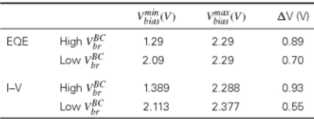
3 JSC in order to measure the EQE of the Ge subcell which, in both cases, shows a relatively low V¡,r. As confirmed by the results shown in Figure 5, the operating point of the Ge subcell is taken away from the breakdown region only if sufficient Vuas is applied. In that case, the cur-rent of the 3JSC is limited by the Ge subcell, and its EQE can be measured as usual (i.e., the MJSC works in the so called Region III of Figure 5). As expected, the empirically detected range of V¡,ias to measure the EQE of the Ge sub-cell in Figure 4 agrees with the V\,ias obtained from the I-V curves of the 3JSC (Figure 5). Table I summarizes the Vuas obtained with the two methods. The data obtained from the I-V curves are more accurate because there are more experimental points than in the data coming from Figure 4.
Table I. Voltage bias range needed to measure the EQE of the
BC, as obtained from the EQE measurements and from the I-V curve of the MJSC. The resulting width of the artifact region
(AV ) is also included.
High vfrc
Low vfrc
High vfrc
Low vfrc
C o o
1.29 2.09 1.389 2.113
C O O
2.29 2.29 2.288 2.377
AV(V) 0.89 0.70 0.93 0.55
Generally speaking, the V\,ias needed for a 3JSC to mea-sure the BC with a low V¡,r in an ideal case (i.e., I-V curve with a flat slope at short circuit conditions) depends pri-marily on both the reverse I-V characteristics of the BC and the Voc of the other subcells that constitute the MJSC. In this case, as the TC and MC are nominally identical in both 3JSC studied, the differences in V\,ias observed between the two 3JSCs are just related to the reverse I-V characteristics of the Ge BC. For MJSCs with low break-down voltage in the BC, the minimum bias voltage (V?™) needed to properly measure the EQE of the BC will be given by the following:
T/miH _ V ^ ^non-limiting SC ,,BC ,-,-.
Vbias ~ 2-^Voc ~ Vbr (ó>
The lower the Vfjs', the higher the VW" is needed, as observed for the two 3JSCs under study in Figures 4 and 5.
Therefore, in order to simplify the task of EQE char-acterization of a BC with unknown properties, instead of performing a "blind" and time-consuming determination of the optimum V¡,¡as, we propose to trace the I-V curve of the MJSC using the light bias to be applied during the EQE measurement of the BC. The optimum V\,ias to properly measure the EQE of the BC is thus determined by the volt-age where the BC really limits, that is, flat region in the I-V curve of the MJSC corresponding to the photo-generated current of the BC (Region III in Figures 4 and 5). In some cases—just due to the intrinsic properties of the BC—there
• „ , , c ,L , • -c x-^ Trnon-limiting SC
will be no need of voltage bias it 2_, *oc <
V, because at 0 V, the BC is current-limiting. On the
con-trary, if jy"c"~ múmg > V^, a Vbias must be applied as what occurred in the two cases described in this paper. A limit case for Ge-based MJSC would be that of a BC with Vbr ~ OV. Given the fact that Voc and FF of Ge subcells at one sun are around 0.2 V and 65%, respectively [22], there is already a narrow voltage range between 0 and the turn on point of the cell ( « 0 . 2 V, depending on the light bias employed during the measurement). Therefore, if we have a breakdown voltage close to zero, the effect of the breakdown will affect the aforementioned narrow flat region, increasing the difficulty of the EQE measurement. Indeed, for the 3JSC analyzed in Figure 4(b), there was just a 0.2 V interval region where a reliable measurement could be performed. Therefore, we empirically establish 1 x 10 cm as a practical upper limit for the doping level of the BC base to allow a correct EQE measurement of the Ge subcell in an MJSC, regardless of other effects that might affect the EQE measurement (shunt resistance or light coupling) [8,10]. For higher doping levels, a straight-forward way to measure the EQE of the subcell will be via an isotype Ge subcell although special procedures as described in Refs [15,16] might be successful and will be explored in a future study.
Regarding the characterization of MJSC with four junc-tions (4JSC) or more with a Ge BC, the effects of the low
than in the 3JSC used here, while the reverse characteris-tic of the low bandgap subcell remains unaltered (i.e., the condition ^ Voc > Vr will be more easily fulfilled). If the BC of the 4JSC is other than a Ge sub-cell, a similar analysis as the one described here should be performed to detect the proper V¡,¡as needed.
4.3. Evolution of the measured EQE in the artifact region
The minimum V¡,¿as at which some response of the EQE of the Ge subcell—the beginning of Region II in Figures 4 and 5—will be measured (Vi • ) is given by the following:
bias
v~~* ^non-limiting SC . ^
br (4)
where AV is the voltage range, where the transition from the MC to the BC takes place (i.e., the width of the artifact region or Region II as indicated in Figures 4 and 5). It depends, as a first approach, on the shape of the reverse characteristics of the BC as well as on the dif-ference between the BC and MC photo-generated current
(IBC a nd IMC> respectively). Table I also summarizes and
compares the empirically detected A V in Figure 4 against the AV obtained with the I-V curves in Figure 5. As shown in the table, the AV determined by both methods are in good agreement.
Special attention is warranted in the case when Vbias is between [Vfc¿aj, V^s] (i-e-> Region II), as defined by
Equations 4 and 3. In this case, the solar cell works in the artifact region, and the EQE measured corresponds to a lin-ear combination of the EQE of two subcells (i.e., MC and BC in our experiments). Notice that, depending on the val-ues of V¡,ias, Vj? , Voc °f the subcells and AV, the artifact region might occur even at short circuit conditions.
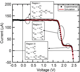
We aim to illustrate such operating conditions with the help of Figure 7 where the I-V curve of the MJSC with the highly doped Ge substrate (i.e., low V¿r in the Ge BC) taken under BC-limiting light bias has been included together with its simulation. The simulation is purely analytical and considers the classic equivalent cir-cuit (irradiance-dependent current source in parallel with two diodes and in series with a resistor) for each subcell in the MJSC, with the particularity of incorporating into the model the breakdown characteristics of the BC (with a simple exponential term). As shown in Figure 7, the fit of the calculated values to the experimental data is very rea-sonable. Accordingly, this model allows us to analyze the working conditions of each subcell along the three differ-ent regions of the I-V curve of the 3JSC (as summarized in the insets of Figure 7), which correspond to the three Regions in Figures 4 and 5. In Region I, despite the BC-limiting light bias conditions are applied, the MC is the current-limiting subcell. This case has already been dis-cussed in detail earlier and essentially implies that the TC approximately operates at its Voc, the BC at a value close to -V£. and, consequently, the MC works at a voltage
200
150
J,100|-I 50
O
-50
-0.5 0.0 0.5 1.0 1.5 Voltage (V)
Figure 7. Simulation of the black I-V curve shown in Figure 5
(i.e., MJSC with BC exhibiting a relatively high breakdown volt-age). In the insets, the operating voltage of each subcell in the
different regions is specified.
jBC\
given by - ( v j ^ - ^ f0) + Vbias (i-e-> m reverse or forward
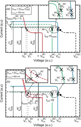
Figure 8 qualitatively explains in more detail the mea-surement artifact that appears when measuring EQE in the artifact region of the I-V curve. In Figure 8(a) and (b), the I-V curve of the MJSC under a light bias that under-illuminates the BC is depicted with a black dashed line. The black circle indicates the operating point of the MJSC—induced by the V\,ias—within the artifact region chosen in the analysis. In addition, the individual I-V curves of the TC (solid blue line), MC (solid green line) and BC (solid red line) have been also included. Figure 8(a) represents the situation when monochromatic light at 750 nm (a wavelength where only the MC should
ü .
v f v f o v l
cv
0TvL
cv
T0f
cVoltage (a.u.)
Voltage (a.u.)
Figure 8. I-V curve of a GalnP/GalnAs/Ge with a low Vbr in the Ge subcell taken under a light bias that under-illuminates the BC (black dashed line). The I-V curves of all subcells have been also included (TC in solid blue line, MC in green solid line and BC in red solid line). The black circle represents the Vb¡as in the artifact region used in the analysis. Panel (a) illustrates the case where monochromatic light at 750 nm is superimposed to the light bias (corresponding shift in the MC curve is shown in a green dashed line) and panel (b) illustrates the case where monochromatic light at 950 nm is superimposed to the bias light (corresponding shift in the BC curved is shown in a red dashed line). The insets include information about how the operating points of the sub-cells change with and without monochromatic illumination with
subscripts 2 and 1, respectively.
show spectral response) impinges on the device. The extra irradiance due to the monochromatic beam shifts the I-V curve of the MC towards higher current values, as indicated by the dashed green I-V curve in Figure 8(a). The insets in Figure 8(a) illustrate how the voltages and currents in each subcell change under this new light bias condition. Subscripts 2 and 1 in the labels used in the insets indicate the situation with and without the monochromatic light, respectively. The increase in the photogenerated current of the MC (i.e., Imono = lfc - lfc) shifts in turn towards lower and higher values (in absolute values) the operat-ing voltages of the TC and BC, respectively, which then increases the operating voltage of the MC. So far, we have the same situation as described in Figure 6. However, as the MC operating point is now at the shoulder of its I-V curve, the MC current is reduced and the operating volt-ages of the TC and BC are correspondingly shifted in the opposite direction. A steady state is ultimately reached (marked with the subscript 2 in the figure), where the MC produces less current out than expected (i.e., Iout < Imono', see Figure 6, for comparison) for the given monochromatic light. Accordingly, the EQE measured will be lower than the EQE measured in Region I.
Figure 8(b) helps to understand the case when, at the same light and voltage bias, the cell is illuminated with a monochromatic beam where only the BC should show response (e.g., 950 nm). In this case, the I-V curve of the BC is shifted upwards (red dashed line in Figure 8(b)). Consequently, as indicated by the insets in Figure 8(b), the operating points of the TC and MC are shifted to lower voltages, which makes the operating voltage of the BC decrease (in absolute value). A steady state is reached (marked with the subscript 2 in the labels used in the insets), where a net increment of the current of the MJSC is produced as a result of the increase of the BC current. In other words, the optical excitation of the BC pro-duces a current measurable with the lock-in amplifier (i.e.,
lout > 0). This current increment detected is lower than
the one that would be produced in Region III, and accord-ingly, the EQE measured will show the same shape but a lower magnitude.
steep and produces more current out, and thus, the magni-tude of the EQE measured in this range will increase in the same proportion. This behavior is exactly what explains the evolution observed in Region II in Figure 4.
4.4. Low VPf versus shunt resistance and luminescent coupling as the origin of the measurement artifact in the
EQE measurement
Traditionally, it has been argued that the low V¿r effect can be treated as a merely shunt effect. From our point of view, this approach is not fully correct and can lead to erroneous conclusions, for instance, when measuring the EQE in the so-called artifact region. Let us summarize some of the main points of the effect of a low V¡,r that make us consider it as a distinct origin of the measurement artifact:
- In strong contrast to the low shunt resistance case, in the presence of a low V¡,r, it is not possible to avoid the measurement artifact by overilluminating the sub-cells not under test, that is, there will be always a Region II as defined in the paper.
- As opposed to the luminescent coupling or low shunt cases, the measurement artifact takes only place for a certain Vuas range (i.e., Region II), irrespective of the light bias condition applied.
- If the Ge subcell shows a sufficiently low V¡,r (such as in the two cases presented in this work), the EQE measured under V\,ias = 0 V and irrespective of the light bias, corresponds to the second limiting junc-tion (MC or TC). This is again a substantial difference in respect to a shunt resistance effect (unless shunt resistance is tremendously low).
- If the case of a low V¡,r is ignored and the EQE mea-surement is performed in the artifact region, which could be at short-circuit conditions, the artifact in the EQE measurement can be erroneously ascribed to the presence of luminescent coupling, leading to a large error when assessing the device performance.
Tracing the I-V curve—under the light bias intended to be applied during the EQE measurement—helps with the detection of difficulties that might arise during the EQE determination. For instance, the I-V curves in Figure 5 indicate a constant current value in Regions I and III. As discussed in the previous sections, Region I and III are dominated by the MC and BC photogenerated current, respectively, and therefore, we can conclude that none of these subcells shows a low shunt resistance. Figure 4 also indicates this fact, because the EQE of the MC and BC in both samples remain constant in some V\,ias range. In the presence of a non-flat slope around the operating point (i.e., in the presence of low shunt resistance), the EQE magni-tude would be lower than expected. Traditionally, it has been attributed a low shunt resistance to the Ge subcell because of its low bandgap [8,13], thus justifying the need of V¡,ias and special light bias conditions during its EQE
characterization [8,13]. While it might be true in some cases, we believe that, in state-of-the-art triple-junction, solar cells grown by highly mature MOVPE processes low shunt resistances are less common. However, a low V¿r in the Ge subcell is more a structural effect arising from the low bandgap of the bottom subcell and the doping ranges used in the design. Therefore, if a low V¡,r (struc-tural effect) is misinterpreted as a low shunt resistance problem (technological effect) important information for the solar cell designer can be lost. The I-V curve of the 3JSC should be traced (under the same light bias condi-tions intended to be applied during the EQE measurement) right before the EQE measurement to detect in advance any problem that might affect the EQE measurement, such as shunt problems or early breakdown in the BC.
Once the problems associated with a low shunt resis-tance and/or a low V? have been discarded, the measure-ment artifacts, if any, can be attributed to other effects such as luminescent coupling between subcells [19]. Indeed, in Figure 1, although the adequate V\,ias n a s been established
by two ways in the 3JSC analyzed, the Ge subcell could not be properly measured (see encircled area in Figure 1). The presence of the so-called measurement artifact can be observed more clearly in Figure 4 at 750 nm for both samples, where the EQE response of the MC is not zero. Although a detailed explanation of this artifact is out of the scope of this paper, the fact that the Ge subcell does not present a low shunt resistance (as seen in Figure 5 and indirectly in Figure 4) and that the artifact increases with light bias of the MC (not shown here) indicate that the ori-gin of the artifact is luminescence coupling from the MC to the BC.
5. CONCLUSIONS
The measurement of the EQE of a subcell in an MJSC with a low breakdown voltage is not a straightforward task. Depending on the breakdown voltage and the Voc of the subcells, not only light bias but also voltage bias must be applied during the measurement. Tracing the I-V curve of the MJSC under the same light bias conditions applied to the EQE measurement will help to determine the proper
Vbias needed (if any), as well as to distinguish whether the
EQE measurement is being affected by shunt problems, early breakdown or luminescent coupling. This is of spe-cial relevance to determine the origin of the measurement artifact that affects the EQE measurement of MJSCs.
ACKNOWLEDGEMENTS
REFERENCES
1. King RR, Law DC, Edmondson KM, Fetzer CM, Kinsey GS, Yoon H, Sherif RA, Karam NH. 40% efficient metamorphic GalnP/GalnAs/Ge multijunc-tion solar cells. Applied Physics Letters 2007; 90(18): 183516.
2. Geisz JF, Friedman DJ, Ward JS, Duda A, Olavarria WJ, Moriarty TE, Kiehl JT, Romero MJ, Norman AG, Jones KM. 40.8% efficient inverted triple-junction solar cell with two independently metamorphic junc-tions. Applied Physics Letters 2008; 93 123505. 3. Sabnis V, Yuen H, Wiemer M. High-efficiency
mul-tijunction solar cells employing dilute nitrides. AIP
Conference Proceedings 2012; 1477(1): 14-19.
4. Chiu P, Wojtczuk S, Zhang X, Harris C, Pulver D, Timmons M. 42.3% efficient InGaP/GaAs/InGaAs concentrators using bifacial epigrowth, In Photovoltaic
Specialists Conference (PVSC), 2011 37th IEEE,
Washington, USA, 2011; 000771-000774.
5. Dimroth F, Grave M, Beutel P, Fiedeler U, Karcher C, Tibbits T, Oliva E, Siefer G, Schachtner M, Wekkeli A, Bett AW, Krause R, Piccin M, Blanc N, Drazek C, Guiot E, Ghyselen B, Salvetat T, Tauzin A, Signamarcheix T, Dobrich A, Hannappel T, Schwarzburg K. Wafer bonded four-junction GalnP/ GaAs//GaInAsP/GaInAs concentrator solar cells with 44.7. Progress in Photovoltaics: Research and
Appli-cations 2014; 22(3): 277-282.
6. King DL, Hansen BR, Moore JM, Aiken DJ. New methods for measuring performance of monolithic multi-junction solar cells, In 2000. Conference Record
of the Twenty-Eighth IEEE Photovoltaic Specialists Conference, Anchorage, Alaska, 2000; 1197-1201.
7. Kurtz SR, Emery K, Olson JM. Methods for analysis of two-functional, two-terminal photovoltaic devices, In 1994 IEEE First World Conference on Photovoltaic
Energy Conversion, 1994., Conference Record of the Twenty Fourth. IEEE Photovoltaic Specialists Confer-ence -1994, Waikola, HI, 1994; 1733-1737.
8. Meusel M, Baurl C, Let'tay G, Bett AW, Warta W, Fernandez E. Spectral response measurements of monolithic GaInP/Ga(In)As/Ge triple-junction solar cells: measurement artifacts and their explanation.
Progress in Photovoltaics: Research and Applications
2003; 11: 499-514.
9. Pravettoni M, Galleano R, Virtuani A, Müllejans H, Dunlop ED. Spectral response measurement of double-junction thin-film photovoltaic devices: the impact of
shunt resistance and bias voltage. Measurement
Sci-ence and Technology 2011; 22(4): 045902.
10. Lim SH, Li J, Steenbergen EH, Zhang YH. Lumi-nescence coupling effects on multij unction solar cell
external quantum efficiency measurement. Progress
in Photovoltaics: Research and Applications 2013;
21(3): 344-350.
11. Steiner MA, Kurtz SR, Geisz JF, McMahon WE, Olson JM. Using phase effects to understand mea-surements of the quantum efficiency and related lumi-nescent coupling in a multijunction solar cell. IEEE
Journal of Photovoltaics 2012; 2(4): 424-433.
12. Steiner MA, Geisz JF, Moriarty TE, France RM, McMahon WE, Olson JM, Kurtz SR, Friedman DJ. Measuring IV curves and subcell photocurrents in the presence of luminescent coupling. IEEE Journal of
Photovoltaics 2013; 3(2): 879-887.
13. Li JJ, Lim SH, Allen CR, Ding D, Zhang YH. Com-bined effects of shunt and luminescence coupling on external quantum efficiency measurements of multi-junction solar cells. IEEE Journal of Photovoltaics
2011; 1(2): 225-230.
14. Paraskeva V, Hadjipanayi M, Norton M, Pravettoni M, Georghiou G E. Voltage and light bias dependent quan-tum efficiency measurements of GalnP/GalnAs/Ge triple junction devices. Solar Energy Materials and
Solar Cells 2013; 116(0): 55-60.
15. Li J-J, Zhang Y-H. Elimination of artifacts in external quantum efficiency measurements for multijunction solar cells using a pulsed light bias. IEEE Journal of
Photovoltaics 2013; 3(1): 364-369.
16. Li J-J, Lim SH, Zhang Y-H. A novel method to elim-inate the measurement artifacts of external quantum efficiency of multi-junction solar cells caused by the shunt effect, In Proceedings of SPIE, San Fracisco, California, USA, 2012; 825616-825616-7.
17. Burdick J, Glatfelter T. Spectral response and IV mea-surements of tandem amorphous-silicon alloy solar cells. Solar Cells 1986; 18(3-4): 301-314.
18. American Standard Test Procedure ASTM E2236—10 standard test methods for measurement of electrical performance and spectral response of nonconcentrator multijunction photovoltaic cells and modules. 19. Steiner MA, Geisz JF. Non-linear luminescent
cou-pling in series-connected multijunction solar cells.
Applied Physics Letters 2012; 100(25): 251106.
20. Barrigón E, Rey-Stolle I, Galiana B, Garcia I, Algora C. GalnP/GalnAs/Ge triple junction solar cells for ultra high concentration, In Proceedings of Spanish
Conference on Electron Devices CDE 2009,
Santi-ago de Compostela, Spain, February 11-13, 2009; 383-386.
21. Neudeck GW. The P-N Junction Diode. Prentice Hall: New Jersey, USA, 1989.
22. Friedman DJ, Olson JM. Analysis of Ge junctions for GalnP/GaAs/Ge three-junction solar cells. Progress in