VI Encuentro Franco-Español de Química y Física del Estado Sólido
VI
emeRencontre Franco-Espagnole sur la Chimie et la Physique de PÉtat Solide
Raman spectroscopy study of group IV semiconductor nanowires
J. Anaya
a, A. Torres
a, A. Martín-Martín
a, O. Martínez
a*, A.C. Prieto
a, J. Jiménez
a,
A. Rodríguez
13, J. Sangrador
13, T. Rodríguez
13"GdS Optronlab, Parque Científico UVa, Edificio I+D, Campus "MiguelDelibes", Paseo de Belén, 1, 47011-Valladolid, Spain Tecnología Electrónica, E.T.S.I.T., Universidad Politécnica de Madrid, 28040 Madrid, Spain.
Abstract
Group IV nanostmctures have attracted a great deal of attention because of their potential applications in optoelectronics and nanodevices. Raman spectroscopy has been extensively used to characterize nanostmctures since it pro vides non destructive information about their size, by the adequate modeling of the phonon confinement effect. However, the Raman spectmm is also sensitive to other factors, as stress and temperature, which can mix with the size effects borrowing the interpretation of the Raman spectmm. We present herein an analysis of the Raman spectra obtained for SiGe nanowires; the influence of the excitation conditions and the heat dissipation media are discussed in order to optimize the experimental conditions for reliable spectra acquisition and interpretation. The interpretation of the data is supported by the calculation of the temperature inside the NWs with different diameters.
Keywords: Si nanowires, Raman spectroscopy, phonon confinement model, heat dissipation, finite element analysis.
1. Introduction
The potential applications of nanoscaled semiconductor structures have raised a great deal of characterization effort. In particular, nanosized structures of group IV semiconductors have been the object of many studies. The properties of those nanostmctures depend on their dimensions; therefore, a great effort is paid to investígate simple ways to determine them. Raman spectroscopy is a very powerful non destructive tool suitable to such study, because of the spectral changes related to the phonon confinement in reduced size structures [1-4]. The study of the lineshape of the first order phonon lines of the Raman spectrum may supply valuable information about the nanostructure size. The Raman spectrum is also sensitive to temperature and stress [5]; therefore, the Raman study
can also provide information about the thermal properties, such as the thermal expansión and the anharmonicity, which are crucial to model the heat dissipation and the thermal induced stresses, necessary to design devices with optimal mechanical and heat transport properties.
The one phonon Raman spectrum of Si nanowires (NWs) has reached a great deal of controversy, because of the discrepancies between the expected and measured lineshapes, failing in the accurate estimation of the NW diameter [1-3]. Different reasons have been argued as possible causes for the inconsistency of the Raman parameters measured in Si NWs. The one phonon Raman lineshape can be modified by inhomogeneous NW diameter distribution [1], Fano scattering from photogenerated carriers [2], and láser induced NW heating [3].
The Raman microprobe works with a relative high láser intensity; the energy absorbed by the sample needs to be dissipated; if the heat evacuation is not efficiently achieved the scattering volume can reach temperatures above the ambient, which deform the Raman bands. Therefore, the thermal conductivity of the probed system has to be considered if one looks for a straightforward interpretation of the Raman data. Usually, nanostructures are embedded in an environment médium, which can have poor thermal conductivity, as is the case of NWs in air. The poor thermal conductivity of the air, and the very small base of the NW in contact with the substrate where they were grown make difficult the heat dissipation from the NW; therefore, one can expect a non-negligible temperature enhancement in the NWs under the láser exposure during the Raman measurement.
We present herein an analysis of the influence of the láser induced heating on the Raman spectrum of SixGei_x
NWs, the temperature distribution inside the NWs is modelled using a finite element analysis procedure.
2. Experimental set-up
SixGei_x NWs were synthesized by Low Pressure Chemical Vapour Deposition (LPCVD) on (100) Si substrates using SÍ2H6 and GeFLi as precursor gases. The Si substrates were dipped in HF, rinsed for 30 s in 3-aminopropyltriethoxysilane (APTES), dried with N2 and subsequently rinsed in a colloidal suspensión of Au particles (30 nm in diameter) for 180 s. The samples were immediately loaded into the LPCVD reactor, where they were annealed at 500 °C for 60 min. The subsequent NW growth process was carried out also at 500 °C for 30 min, using GeFLi flows between 2 and 20 sccm and SÍ2H6 flows between 8 and 2 sccm, in such a way that the flow ratio GeH4:Si2H6 was varied between 0.25 and 10. The total pressure was maintained at 400 mTorr.
The Raman spectra were acquired with a Labram UV-HR 800 Raman spectrometer from Jobin Yvon. The measurements were done in air and with the NWs submerged in deionized water. The excitation was done with an Ar láser (514.5 nm) or a He-Ne láser (632.8 nm), using a 0.95 numerical aperture 100X objective; excitation láser intensities on the sample surface, up to 100 kWcm" , were used. The first order Raman spectrum of Si presents a band at -520 cm" , while the Raman spectrum of SiGe presents three bands at -300, -400 and -500 cm" , attributed to the Ge-Ge, Si-Ge and Si-Si vibrations, respectively; the peak position and width of each band depend on the Ge fraction, with a shift to low wavenumbers and an increase of the asymmetry of the band with the increase of the Ge contení, due to structural disorder.
3. Results
The NWs form tangles of wires, as observed in the scanning electrón microscope (SEM), Fig.l. Typical NWs had diameters ranging from 15 to 120 nm and several \im length, depending on the growth conditions - it has been observed that the diameter nearly does not change with the Ge contení. However, the crysíalline core should be smaller, since usually a íhick SiOx shell is presenl. The circle in Fig. 1 represenls íhe láser beam on íhe focus, which means íhal only a reduced number of wires are probed in a Raman measuremenl.
*v, ti?:7!
KÉIÉW
¡fcS»
Figure 1. SEM image of Si NWs. The circle represents the láser beam at the focus. The zoom shows that only a few NWs (4 in this case) with different diameters are excited by the láser beam.
440 460 460 600 520 Raman shift (crrw}
11-B-^N^^yM^^wy
1.0- l/íjfM^MV ¿ttftftylWlHftflfW I
^AtVlTAl Oí /
400 420 440 460 480 600 620
Raman shift (cm~1)
Figure 2. Raman spectra in air (a), and in water (b). The láser intensities are 10 kWcm" (only in a), 25 kWcm" 100 kWcm"2. The control spectrum is also shown in (b).
50 kWcm"2 and
The average size of NWs can be determined using a phenomenological phonon confínement model [7, 8]. These models are based on the uncertainty of the phonon momentum, because of the reduced size of the structures. In reduced size structures phonons with q^0 are allowed to contribute to the Raman spectrum. Assuming a Gaussian localization factor [7, 8] the Raman intensity can be expressed as:
l{a>,L)
X\e^-í£
d3qstof+pf
(1)where co(q) is the phonon dispersión ñmction and T0 is the full width at half máximum (FWHM) of the bulk
o ( q , T) = (A + { A2 - B[l - eos (jiq )] }1 / 2 ) 1/2 (2)
where A(T) and B(T) are determined from the phonon dispersión curve [9]. The Raman phonon bands depend on the temperature because of the thermal expansión and the anharmonicity of the vibrational potential energy [5, 10-12]. The dependence of the Raman spectrum with temperature for bulk material was previously obtained on the control Si wafer. The variation of co and T0 with temperature were approached to a linear function:
m (cnT1) = 521.9 - 0.0242 T (°C)
(3) r0 (cnT1) = 2.8 + 0.0102 T (°C)
The temperature coefficients of Eq. 3 for phonons with q^0 are not available, therefore the full phonon branch was assumed to follow Eq. 3. Note that this is a first approximation, because one can expect a variation of the anharmonic constants of nanostructures respect to the anharmonic constants of the bulk material. To the best of our knowledge, no reliable data exist about the influence of the size on the anharmonicity and the thermal expansión of Si NWs. Nevertheless, a dependence of the anharmonic coefficients with nanocrystal size was reported for CdSe nanocrystals embedded in germanate glass [13].
Using this model we have estimated the effect of the temperature in the Raman spectra of the NWs. Figure 3 shows the Raman spectra shape obtained for a NW with a diameter of 8 nm at different temperatures. The Raman band shifts to lower wavenumbers and broadens with the increase of temperature, becoming more symmetric respect to the Raman lineshape due to puré phonon confmement.
500 505 510 515 520 525
Raman frequeney (cni1)
Figure 3. Calculated Raman spectra taking account of temperature (for a NW with a diameter of 8 nm).
The experimental spectra with the NWs in air cannot be fitted using a single NW diameter and the temperature effect. In fact, the spectra obtained at high láser power, Fig. 2a, do not look symmetric as expected for NWs at high temperature. The line shape of the experimental spectra can only be accounted for on the basis of an inhomogeneous temperature distribution inside the scattering volume. Adu et al. [14] modeled the Raman spectra taking account of a temperature gradient inside the láser excited región of the NWs; they assumed a fixed NW diameter and needed a very large axial temperature variation (T-100 K).
to the fact that one of the ends is in contact with the substrate, while the other is not); it should be noted that this gradient is even lower for NWs with larger diameter; these gradients cannot account by themselves for the anomalous broadening of the experimental Raman bands. However, these data provide the information necessary to interpret the Raman spectra of discrete sets of NWs with dispersed diameters. Under this approach, one can fit the experimental Raman bands considering a reduced number of NWs of different diameters, and therefore, different temperatures induced by the láser beam excitation. Figure 4b shows the fit of the experimental Raman spectrum considering the contribution of four wires with diameters of 20, 30, 40, and 100 nm, which according to the data of Fig. 4a, estimated for a láser intensity of 100 kWcm" (equivalent to our experimental conditions), reach temperatures around 400, 325, 250, and 150 °C. The contribution of each NW was weighted according to its corresponding contribution to the scattering volume in order to get the best fit [16].
_ 700
o E50
J 600
£ 550
soo
350
40
NW diameter (nm)
480 490 500 510 520 530 540 wavenumber (cm"1)
Figure 4. a) Calculated temperature induced by the láser beam as a function of the NWs diameter for an incident láser intensity of 100 kWcm"2 (Gaussian distribution). The inset shows the axial temperature distribution inside the área excited by the láser beam
in a 20 nm diameter wire. b) Experimental (dots) Raman spectrum of NWs in air (láser intensity 100 kWcm"2), and calculated (line) spectrum considering four wires with different diameters and their corresponding láser beam induced temperatures.
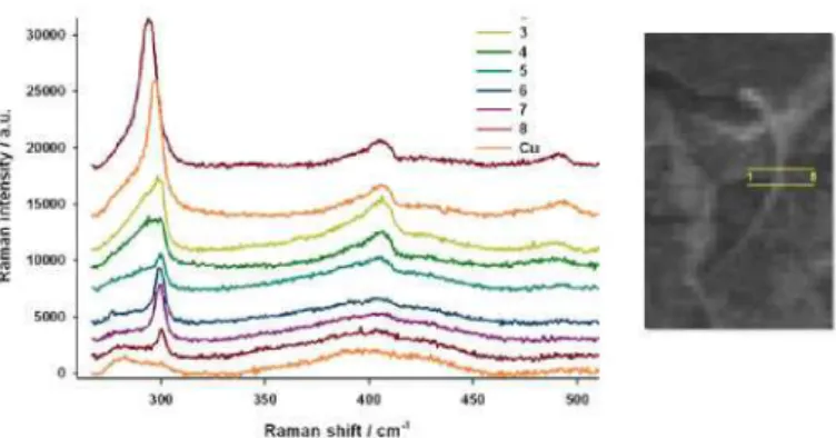
Taking account of the effect of the heating introduced by the láser beam on the NWs as a function of their diameter, we started to interpret the Raman spectra of SiGe NWs grown by the same method. Figure 5 shows the Raman spectra (A,=632.8 nm) obtained by transversally crossing a SiGe NW (step of 250 nm). The NW, with an apparent diameter of 200 nm, was isolated by ultrasounds. The lineshape of the Raman band varíes notably, which should be due to the effect of the increased temperature caused by the láser spot. At present we are performing calculations by means of finite element analysis of the variation of the temperature as a function of the position of the láser spot to account for these results.
3. Conclusions
In this work we study, both experimental and theoretically, the Raman spectra of SixGei_x NWs taking account of
300 350 400 450 500 Raman -.rnft .' cni
Figure 5. Raman spectra obtained crossing a SiGe NW (step size 250 nm), as shown in the optical image on the right. The spectrum corresponding to the copper (Cu) grid holder where the NW was deposited is also shown.
Acknowledgements
This work was ñmdedby the Spanish Government (MAT-2007-66181) andby Junta de Castilla y León(VA051A06 -GR202).
References
[I] Y. Cui and C. Lieber, Science 291, 851 (2001).
[2] S. Bhattacharyya and S. Samui, Appl. Phys. Lett. 84, 1564 (2004).
[3] R. Gupta, Q. Xiong, C.K. Adu, UJ. Kim, and P.C. Eklund, Nano Lett. 3, 627 (2003).
[4] H. Scheel, S. Reich, A.C. Ferrari, M. Cantora, A. Colli, and C. Thomsen, Appl. Phys. Lett. 88, 233114 (2006).
[5] J. Jiménez, I. de Wolf, and J.P. Landesman, in "Microprobe Characterization of Semiconductors"; vol.17 of Optoelectronic properties of semiconductors and superlattices, ed. by J. Jiménez (Taylor and Francis, New York 2002), ch.2.
[6] H.D Young, University Physics, 7a Ed., Addison Wesley, 1992.
[7] H. Richter, Z.P. Wang, and L. Ley, Solid State Commun. 39, 625 (1981). [8] I.H. Campbell and P.M. Fauchet, Solid State Commun. 58, 739 (1986). [9] S. Wei and MY. Chou, Phys. Rev. B 50, 2221 (1994).
[10] P. Mishra and K.P. Jain, Phys. Rev. B 62, 14790 (2000).
[II] S. Piscanec, M. Cantora, A.C. Ferrari, JA. Zapien, Y. Lifshitz, S.T. Lee, S. Hofman, and S. Robertson, Phys. Rev. B 68, 241312 (R) (2003).
[12] J. Jiménez, A. Torres, E. Martin, and J.P. Landesman, Phys. Rev. B 58, 10463 (1998).
[13] M.J. ¡Constantinovic, S. Bersier, X. Wang, M. Hayne, P. Lievens, R.E. Silverans, and V.V. Moshchalkov, Phys. Rev. B 66, 161311(R) (2002).
[14] K.W. Adu, H.R. Gutiérrez, U.J. Kim, and P.C. Eklund, Phys. Rev. B 73, 155333 (2006). [15] D. Li, Y. Wu, P. Kim, L. Shi, P. Yang, and A. Majumdar, Appl. Phys. Lett. 83, 2934 (2003).