Low-Profile Dual Circularly Polarized Antenna Array
for Satellite Communications in the X Band
Andrés García-Aguilar, José-Manuel Inclán-Alonso, Lucía Vigil-Herrero, José-Manuel Fernández-González, and
Manuel Sierra-Pérez
, Senior Member, IEEE
Abstract—A planar antenna is introduced that works as a portable system for X-band satellite communications. This antenna is low-profile and modular with dimensions of cm. It is composed of a square array of 144 printed circuit elements that cover a wide bandwidth (14.7%) for transmission and reception along with dual and interchangeable circular polarization. A radiation efficiency above 50% is achieved by a low-loss stripline feeding network. This printed antenna has a 3 dB beamwidth of 5 , a maximum gain of 26 dBi and an axial ratio under 1.9 dB over the entire frequency band. The complete design of the antenna is shown, and the measurements are com-pared with simulations to reveal very good agreement.
Index Terms—Antenna arrays, dual-polarized antennas, mi-crostrip antennas, satellite communication.
I. INTRODUCTION
N
EW fixed and mobile satellite systems [1] require an-tenna systems that must be portable, low-profile and light-weight to provide ubiquitous and high-capacity communica-tions-on-the-move. Planar antennas are perfect candidates for meeting these specifications. Slots [2] are often used as radi-ating elements, but microstrip patches [3] are preferable due to their ease of manufacturing and lower weight. Although phased arrays [4], [5] can reconfigure an antenna system to point in a desired direction, low-cost systems are in high demand. Hybrid mechanical/electronic steerable solutions reduce costs [6] but are more expensive and difficult to design than a fixed beam array antenna. The main goal of this research is to design and measure a printed array antenna that could be used as a portable man-pack with a high efficiency and cover a wide frequency band for personal satellite communication services.Microstrip arrays exhibit low efficiencies (typically less than 50%) due to ohmic/dielectric losses and parasitic radiation in
Manuscript received June 27, 2011; revised September 16, 2011; accepted October 26, 2011. Date of publication March 09, 2012; date of current version May 01, 2012. The simulations performed in this work were realized using CST Microwave Studio Suite 2011 under a cooperation agreement between Com-puter Simulation Technology (CST) and the Technical University of Madrid (UPM). The project was led by the Technical University of Madrid and Antenas Moyano S.L. with the support of the Spanish Education Ministry (Comisión In-terministerial de Ciencia y Tecnología) under reference TEC2008-06736/TEC and a Spanish Government Grant (FPI under reference BES-2009-021462). This work was supported in part by the U.S. Department of Commerce under Grant BS123456.
The authors are with the Radiation Group, Technical University of Madrid (Universidad Politécnica de Madrid-UPM), Madrid 28040, Spain (e-mail: [email protected]; [email protected]; [email protected]; [email protected]; [email protected]).
Color versions of one or more of the figures in this paper are available online at http://ieeexplore.ieee.org.
Digital Object Identifier 10.1109/TAP.2012.2189729
the feeding network and also due to surface wave excitations in the dielectric substrate [7], [8]. Some serial waveguide-fed structures [9] are able to obtain higher efficiencies but increase the weight and provide narrow bandwidths. In this work, by de-signing a low-loss stripline corporative network and performing active impedance matching for the microstrip patch, the mea-sured radiation efficiency remains between 50% and 60%, de-pending on the frequency and polarization. This antenna works in the X band from 7.25 to 8.4 GHz, which represents a 14.7% relative bandwidth.
The antenna was designed to be planar, compact, modular and dual circular polarized for transmission (Tx) and reception (Rx) bands simultaneously. It is composed of a square planar array of 12 12 double-stacked microstrip patches fed by two via holes and a hybrid circuit to create two orthogonal modes in the microstrip patch and the dual circular polarization [10]. More-over, to reinforce the circular polarization the sequential rotation technique is used between 2 2 patches. The array is divided into 9 identical subarrays of 4 4 radiating elements, making it possible to separate the manufacturing of the subarrays from that of the global signal distribution network, simplifying the corporative network and providing a modular structure suitable to a serial fabrication process. Planar multilayer antenna tech-nology [11], [12] is appropriate for new subarray antenna archi-tectures that integrate the radiating elements with the associated active and passive circuitry. In this system, each subarray forms a multilayer board, making it simple to update the antenna with electronic scanning capabilities.
The subarray feeding network is fabricated using microstrip technology for right-handed and left-handed circular polariza-tion (RHCP and LHCP, respectively). The global distribupolariza-tion network is a low-loss stripline located under the subarrays. This type of feeding network involves a trade-off between the sim-plicity of exciting the radiating elements using printed circuits and loss reduction by separating the distribution network into a structure designed to realize low losses. The power distribu-tion network is connected to each subarray through SMP-type coaxial connectors, and there are two global ports (input/output) with SMA-type connectors, one for each polarization.
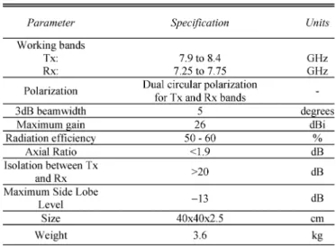
Table I summarizes the main characteristics of the antenna. The paper is organized as follows. Section II describes the composition and the different layers of this antenna system. Section III presents the subarray design and measurements of the radiating element, the hybrid circuit and the array unit cell. In Section IV, the design and measurements of the stripline cor-porative network are shown. Section V shows measurements of the prototyped antenna. Finally, conclusions are drawn and pre-sented in Section VI.
II. ANTENNADESCRIPTION
The antenna is formed by an array of 12 12 microstrip patches and is divided into 9 equal subarrays of 4 4 ele-ments. The distance between patches is 33 mm. Fig. 1 shows a schematic of the array composition and the different layers of the antenna. The upper layer corresponds to the subarrays, while the bottom layer is the excitation network. The former has a mi-crostrip technology feeding structure with one layer for RHCP and LHCP that excite the microstrip patches through two via holes. The patch and subarray network layers exhibit a unique structure in which they are interconnected to the global distribu-tion network through two SMP-type coaxial connectors. To pro-vide robustness, a 5 mm foam sheet was added above the upper dielectric layer. The global power distribution network is com-posed of a stripline layer for RHCP and LHCP and two general SMA input/output ports, one for each polarization. The stripline network is designed for low losses and is protected by walls on both sides to prevent the excitation of undesired modes. The an-tenna is designed for a reference input impedance of 50 .
To achieve a lower side lobe level (SLL), excitation tapering was implemented in the subarrays. Thus, the signal amplitudes of each subarray are not equal but do have symmetry with respect to the two main antenna axes.
III. SUBARRAYCONFIGURATION
A. Radiating Element, Hybrid Circuit and Unit Cell
The radiating element in Fig. 2 is a double-stacked microstrip patch that covers a wide frequency band and is excited by two via holes with a branch-line coupler (BLC) to generate circular polarization [10]. This printed element must work over a large bandwidth (14.7%), and therefore a thick lower substrate (1.58 mm) is required. The dielectric supports surface waves that will degrade the antenna efficiency by increasing the coupling be-tween the array elements. Nevertheless, such a coupling can be compensated by designing the radiating element in an array en-vironment and supposing that the element is immersed in an infinite two-dimensional periodic structure. This assumption is valid for the central radiating elements in the real array. It will
Fig. 1. Printed antenna structure. (a) Perspective view with subarray detail. (b) Side view and multilayer scheme.
Fig. 3. Isolated radiating element input reflection coefficient.
be less accurate for the edge patches but is sufficient for the de-sign of this antenna, as will be shown later. Other options are available to reduce the couplings, such as using an impedance matching network in the microstrip feeding structure [13], de-signing a cavity microstrip antenna as a radiating element [14] or including a structure with a forbidden frequency band [15] to cut off dielectric surface waves.
The double-stacked patch optimization is done using a FDTD full-wave simulator where the thickness of the substrates is kept fixed and the patch diameters (that control the frequency resonance) and the via hole positions (that match the microstrip feeding network and the patch impedances) are the optimization parameters. The goal is to achieve an input reflection coefficient lower than 15 dB, and an axial ratio better than 3 dB. Periodic boundary conditions are used to optimize the element within an infinite planar array.
The radiating element is designed for a reference impedance of 40 due to a restriction in the fabrication of the minimum line width, because one of the BLC microstrip lines is in the manufacturing limit of 0.2 mm. Fig. 3 exhibits the simulated and measured reflection coefficient for an isolated radiating element, where a very good agreement is met. Thus, it is shown that one single element can cover the working bandwidth properly.
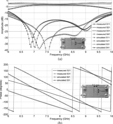
The BLC can work with dual circular polarization, i.e., with simultaneous RHCP and LHCP, in the same band as the patches. Thus, a three-branch periodic 3 dB BLC was designed [16] to cover the same bandwidth. However, a conventional con-figuration requires an area of 13.2 cm , which is large com-pared to the radiating element and the subarray; therefore, this BLC was miniaturized using the equivalence between a transmission line and a line with an open-ended shunt stub [17]. Other configurations have been investigated, including fractal shapes [18] and interdigitally-coupled lines [19], but this so-lution was chosen due to its simplicity and quality. The com-pact BLC is shown in Fig. 2(b), and Fig. 4 presents a compar-ison between the simulated and measured S-parameters. The BLC works properly, and the discrepancies between simula-tions and measurements are caused by the SMP connectors, whose effect is not included in simulations. The area is reduced by about 35%, diminishing the couplings inside the subarray feeding network.
To improve the circular polarization quality, the sequential rotation technique [10] was implemented in each 2 2 element, shown in Fig. 5. Each patch was rotated 90 and excited by a
Fig. 4. Miniaturized BLC S-parameter measurements. (a) Amplitude. (b) Phase.
Fig. 5. Unit cell. (a) Stacked microstrip patches. (b) Microstrip feeding network.
signal phase-shifted 90 relative to that of the previous element, as indicated in Fig. 5(a). These 2 2 radiating elements form the array unit cell. Such a configuration allows an improvement of approximately 20 dB in the copolar-crosspolar ratio.
B. Subarray
Fig. 6. Subarray microstrip feeding network.
Fig. 7. Simulated embedded input reflection and coupling coefficients among some subarray elements for RHCP.
Hence, there are 9 equivalent subarrays with a total size of 13.1 13.1 0.61 cm that comprise a unique multilayer board and are interconnected with a power distribution net-work through SMP connectors (surface mount) and vertical transitions. Such connectors and vertical transitions exhibit measured transmission losses of approximately 1 to 2 dB, which will reduce the realized gain in the radiation pattern mea-surements compared with simulations, in which their effects have not been considered.
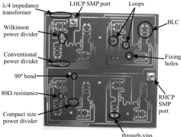
Fig. 6 shows the subarray feeding network prototype. Unit cell is repeated four times and joined together in phase through two different paths, one for each polarization. Loops help to carry the correct phase at each point regarding with the sequential rotation and the polarization. Wilkinson power dividers before the BLC eliminate reflected signals from the patches, and compact size conventional power dividers reduce the couplings among the microstrip lines. impedance transformers are placed at each SMP port to change the line characteristic impedance from 40 to the final 50 .
Fig. 7 depicts the simulated input match for a central ele-ment within the subarray, as well as the coupling among sur-rounding patches, where microstrip network has not been in-cluded. Coupling coefficients between radiating elements are kept under 20 dB revealing that this effect is not increasing the losses in the antenna due to surface waves propagation. Mainly,
Fig. 8. Measured and simulated subarray results. (a) Gains of copolar and crosspolar components. (b) Axial ratios.
the coupling between microstrip lines will degrade the system behavior.
Because the LHCP network has a longer path than the RHCP one, higher losses, stronger couplings and worse input impedance matching will be expected in the former. Fig. 8 shows a comparison of the measured and simulated gains and axial ratios. A maximum gain of 18.2 dBi for RHCP and approximately 17 dBi for LHCP was measured for the copolar component in the central band. The minimum measured copolar gain is approximately 16.6 dBi for RHCP and 15.2 dBi for LHCP in the upper extreme band. LHCP displays between 1.2 and 1.4 dB of extra losses compared with RHCP. For RHCP, the losses compared to simulations are 1.5 dB in the center frequency and approximately 2.5 dB in the upper frequency. The copolar-crosspolar ratio is greater than 22.5 dB at all frequencies. The axial ratios of both polarizations remained below 1.4 dB over the entire bandwidth and agreed quite well with simulations.
The differences between simulations and measurements are more severe for LHCP due to higher losses and couplings in its feeding network. Because of these differences and unmodeled SMP connector losses, LHCP displayed worse behavior than RHCP.
To complete the set of subarray measurements, Fig. 9 shows the measured radiation patterns at 7.9 GHz for both polariza-tions and for three cuts on the axis (azimuth).
IV. POWERDISTRIBUTIONNETWORK
Fig. 9. Measured radiation patterns of the subarray at 7.9 GHz for (a) RHCP and (b) LHCP. In the legend, CP refers to the copolar field component and XP to the crosspolar field component.
Fig. 10. Low-loss stripline. (a) Multilayer scheme side view. (b) Transition from stripline to SMP-type connector. (c) Transition from stripline to SMA-type connector.
and thus maximize the efficiency. The stripline is formed by a metalized line in a thin substrate suspended in air between two metallic plates, which act as ground planes. The air gap must be thick if low losses are required. A quasi-TEM mode is propagated through this transmission line utilizing the presence of two different dielectrics (PTFE-glass and air). However, to avoid the propagation of an undesired resonant TE mode, which can be excited by irregularities in the structure, the stripline is protected by surrounding it with metallic walls. This metallic structure also provides stiffness to the suspended stripline.
Fig. 11. Printed power distribution network board with aluminum walls.
The final structure is schematized in Fig. 10(a). The distance between the walls that shield the line has to be sufficiently small to prevent interference with the quasi-TEM mode and must also cut off the non-desired TE mode. A distance of 16 mm was set, and it was observed that the TE mode begins propagating above 9 GHz.
Transitions between the stripline and each subarray are performed through SMP-type connectors. There are two inputs/outputs in the antenna, one for each polarization, each of which has an SMA coaxial connector. These vertical tran-sitions break the symmetry of the line, and to prevent the generation of a TE mode, it is necessary to protect them with a short-ended pseudo-waveguide that cuts off the TE mode. Fig. 10(b) and (c) show the protected transitions SMP and SMA, respectively. The losses are around 0.7 and 0.2 dB for the SMP and the SMA transitions, respectively. In addition, the SMP connectors must be mounted over a microstrip line; therefore, a transition between the stripline and microstrip line has to be designed to guarantee good impedance matching. The widths of the stripline and microstrip line are quite different, and the transition has to change the line width gradually as shown in Fig. 10(b).
Finally, the corporative network is depicted in Fig. 11, where the coaxial to stripline transitions are detailed. The network has two paths printed on the same layer, one for each polarization. The design has been performed, with a reference impedance of 50 , branch by branch using loops and unbalanced power dividers to get the proper phase and amplitude in the subarray inputs, because the excitation levels of the subarrays are not equal, as was noted in Section II.
Fig. 12. Measured transmission parameters of RHCP to each subarray. (a) Am-plitude. (b) Phase.
Fig. 13. Measured transmission parameters of LHCP to each subarray. (a) Am-plitude. (b) Phase.
Fig. 14 exhibits the measured transmission losses of both polar-izations, which are approximately 1.4 dB for LHCP and 1.8 dB for RHCP. Losses are higher in the latter because the paths are longer.
Fig. 14. Average measured transmission losses of both polarizations in the power distribution network from SMA global connectors to SMP subarray input ports.
Fig. 15. (a) Antenna system with radome. (b) Antenna in anechoic chamber, frontal view. (c) Antenna in anechoic chamber, back view with SMA connec-tors.
V. RESULTS ANDDISCUSSION
The complete antenna was measured successfully. Fig. 15 de-picts the final antenna system with a PVC radome mounted in an anechoic chamber for measurement acquisition.
Fig. 16 shows the measured S-parameters of the two SMA ports. The input reflection coefficient remains under 10 dB over the entire band, which is sufficient to ensure a radiation efficiency above 50%. The observed peaks are mainly due to strong couplings in the subarray feeding network. The coupling between ports is under 20 dB in the working band.
Fig. 16. Measured S-parameter amplitudes for the antenna, where port 1 is the SMA LHCP input/output and port 2 is the SMA RHCP input/output.
Fig. 17. Measured and simulated antenna results. (a) Gains of the copolar and crosspolar components. (b) Axial ratios.
transmission losses due to its longer paths, as was already men-tioned in Sections III and IV. The measured and simulated gains for RHCP, exhibit 3.5 dB of difference at the center frequency and approximately 5.2 dB at the upper frequency. These losses are primarily due to the transitions between the SMA/SMP connectors and the printed lines, which were not considered in the simulations. Furthermore, the simulations were performed without the global stripline network, and the losses in Fig. 14 were therefore not included and must be subtracted.
The measured gain guarantees a radiation efficiency of 50% for this antenna system, measured at 8.25 GHz for LHCP. The maximum measured radiation efficiency is 60% for the RHCP port at 7.75 GHz. Finally, the copolar-crosspolar ratio is above 20 dB over the entire band, and the axial ratio remains below 1.9 dB for both polarizations.
Figs. 18, 19 and 20 show the measured radiation patterns at 7.25, 7.9 and 8.4 GHz, respectively, for the two polarizations
Fig. 18. Measured radiation pattern of the antenna at 7.25 GHz for (a) RHCP and (b) LHCP. In the legend, CP refers to the copolar field component and XP to the crosspolar field component.
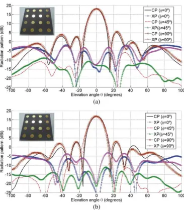
Fig. 19. Measured radiation pattern of the antenna at 7.9 GHz for (a) RHCP and (b) LHCP. In the legend, CP refers to the copolar field component and XP to the crosspolar field component.
Fig. 20. Measured radiation pattern of the antenna at 8.4 GHz for (a) RHCP and (b) LHCP. In the legend, CP refers to the copolar field component and XP to the crosspolar field component.
and for three cuts on the -axis. SLL values are less than 15 and 13 dB for RHCP and LHCP, respectively, at all frequencies.
high efficiency and wide frequency band.
The array is divided into 9 equal subarrays of 4 4 double-stacked microstrip patches. A BLC allows it to have dual cir-cular polarization, which was miniaturized to save space in the subarray feeding network and reduce the couplings between the lines. The subarrays have microstrip feeding structures, and each subarray is fed with a low-loss protected stripline. Tran-sitions between subarrays and the global corporative network are performed through SMP-type coaxial connectors. There are also two SMA ports, one for each polarization, which are the global input/output. These transitions have to be treated care-fully to avoid the excitation of undesired modes. The sequential rotation technique is applied between the two by two elements to form the unit cell of the array and provide more pure circular polarization. To minimize the SLL, the subarrays have excita-tion levels that decrease from the center to edges.
Measurements show that the gain is between 23.8 and 26.2 dBi, the radiation efficiency is between 50% and 60%, the copolar-crosspolar ratio is above 20 dB, the axial ratio is below 1.9 dB and the SLL is less than 13 dB. The measured and simulated results are in very strong agreement given that the effects of the global distribution network and transitions between the coaxial connectors and lines are not considered in the simulations. Therefore, because the measured losses of such transitions are around 1 or 2 dB and the stripline network losses are between 1.4 and 1.8 dB, differences of approximately 3 to 6 dB between simulations and measurements of the complete antenna were expected.
ACKNOWLEDGMENT
The NY substrate used in the prototypes was kindly provided by NELTEC S.A.
REFERENCES
[1] B. G. Evans, Satellite Communication Systems, 3rd ed. London, U.K.: The Institution of Engineering and Technology, 2008. [2] M. Sierra-Castañer, M. Vera-Isasa, M. Sierra-Pérez, and
J. L. Fernández-Jambrina, “Double-beam parallel plate slot antenna,”
IEEE Trans. Antennas Propag., vol. 53, no. 3, pp. 977–984, Mar. 2005.
[3] A. Stark, A. Dreher, H. Fischer, A. Geise, R. Gieron, M. Heckler, S. Holzwarth, C. Hunscher, A. F. Jacob, K. Kuhlmann, O. Litschke, D. Lohmann, W. Simon, F. Wotzel, and D. Zahn, “SANTANA: Advanced electronically steerable antennas at Ka-band,” inProc. 3rd EuCAP, Berlin, Germany, 2009, pp. 471–478.
[4] D. A. Bajgot, “Development of a low-cost, man-portable, phased array X-band radar,” inProc. 2010 IEEE Int. Symp. ARRAY, Waltham, MA, 2010, pp. 183–188.
[5] W. H. Theunissenet al., “Development of an X-band phased array an-tenna,” inProc. 2011 IEEE Int. Symp. ARRAY, Waltham, MA, 2010, pp. 211–218.
Handbook. Norwood, MA: Artech House, 2001, ch. 2, pp. 493–532. [11] L. Infante, A. De Luca, and M. Teglia, “Low-profile ultra-wide band antenna array element suitable for wide scan angle and modular sub-array architecture,” inProc. 2010 IEEE Int. Symp. ARRAY, Waltham, MA, 2010, pp. 157–163.
[12] Y. Kuwahara, Y. Matsuzawa, H. Kitahara, and M. Haneishi, “Phased array antenna with a multilayer substrate,”IEE Proc. Microwaves, An-tennas Propag., vol. 141, no. 4, pp. 295–298, Aug. 1994.
[13] H. F. Pues and A. R. Van de Capelle, “An impedance-matching technique for increasing the bandwidth of microstrip antennas,”IEEE Trans. Antennas Propag., vol. 37, no. 11, pp. 1345–1354, Nov. 1989. [14] N. C. Karmakar, “Investigations into a cavity-backed circular-patch
an-tenna,”IEEE Trans. Antennas Propag., vol. 50, no. 12, pp. 1706–1715, Dec. 2002.
[15] D. Sievenpiper, L. Zhang, R. F. J. Broas, N. G. Alexopolous, and E. Yablonovitch, “High-impedance electromagnetic surfaces with a for-bidden frequency band,”IEEE Trans. Microw. Theory Tech., vol. 47, no. 11, pp. 2059–2074, Nov. 1999.
[16] G. L. Matthaei, L. Young, and E. M. T. Jones, “TEM-mode, coupled-transmission-line directional couplers and branch-line direcitional couplers,” inMicrowave Filters, Impedance-Matching Networks, and Coupling Structures. Norwood, MA: Artech House, 1980, ch. 13, pp. 775–842.
[17] W.-L. Chen and G.-M. Wang, “Exact design of novel miniaturised fractal-shaped branch-line couplers using phase-equalising method,”
IET Microwaves, Antennas Propag., vol. 2, no. 8, pp. 773–780, Dec. 2008.
[18] Z. Liu and R. M. I. Weikle, “A compact quadrature coupler based on coupled artificial transmission lines,”IEEE Microw. Wireless Compon. Lett., vol. 15, no. 12, pp. 889–891, Dec. 2005.
[19] C. Tang and M. Chen, “Synthesizing microstrip branch-line couplers with predetermined compact size and bandwidth,”IEEE Trans. Mi-crow. Theory Tech., vol. 55, no. 9, pp. 1926–1934, Sep. 2007.
Andrés García-Aguilarwas born in Madrid, Spain, in 1984. He received the B.Sc. and M.Sc. degrees in telecommunications engineering from Technical University of Madrid (UPM), Spain, in 2008 and 2009, respectively, where he is currently working toward the Ph.D. degree in the Radiation Group, Signals, Systems and Radiocommunications Depart-ment as a recipient of a Spanish Ministry of Science and Innovation scholarship (2009–2013).
In 2011, he was with the Faculty of Electrical Engineering and Computing, University of Zagreb, Croatia, as invited Ph.D student. His research interests are planar and conformal antenna design, numerical methods and metamaterials applied to antenna and microwave device analysis and synthesis.
José-Manuel Inclán-Alonsowas born in Madrid, Spain, in 1986. He received the B.Sc degree in telecommunications engineering from Technical University of Madrid (UPM), Spain, in 2010, where he is currently working toward the Ph.D degree in the Radiation Group in the Signals, Systems and Radiocommunications Department.
Lucía Vigil-Herrerowas born in Madrid, Spain, in 1981. She received the B.Sc. degree in telecommu-nications engineering from Technical University of Madrid, Spain, in 2011.
Her main research activity is in antenna syn-thesis and design for satellite communications at microwave frequencies.
José-Manuel Fernández-González was born in Lausanne, Switzerland, in 1977. He received the Diplôme d’Ingénieur en Électricité from the École Polytechnique Fédérale de Lausanne (EPFL), Switzerland, in 2003. From October 2002 to March 2003, he completed the M.S. thesis as an Erasmus program student in the Radiation Group, Signals, Systems and Radiocommunications Department at Technical University of Madrid, where he received the Ph.D degree in the Radiation Group, Signal, Systems and Radiocommunications Department. From January to May 2006, he has spent three months abroad as a guest Ph.D student at “Centre de Recherches Poly-Grames” of l’École Polytechnique de Montréal, QC, Canada. From September to December 2007, he was with the Antenna Group, Signals and Systems Department at Chalmers University of Technology, Göteborg, Sweden as invited Ph.D student. Since 2009, he is a postdoctoral researcher in the Radiation Group, Signals, Systems and Radio-communications Department at Technical University of Madrid. His current re-search interest is in the field of metamaterial structures with emphasis on planar antenna applications. He has been active in the area of antenna synthesis and de-sign, and participates actively in national and international investigation projects for companies.
Dr. Fernández has been the recipient of a Spanish Ministry of Education and Science scholarship (2006–2010).
Manuel Sierra-Pérez (M’90–SM’98) was born in Zaragoza, Spain, in 1952. He received the M.S. degree (Telecommunication engineer) and the PhD degree from the Technical University of Madrid (UPM), Spain, in 1975 and 1980, respectively.