Thermomechanical Issues of High Power Laser Diode
Catastrophic Optical Degradation
Jorge Souto, José Luis Pura and Juan Jiménez
GdS Optronlab, Ed. LUCIA, Paseo de Belén, s/n, Universidad de Valladolid, 47011 Valladolid, Spain
Abstract
Catastrophic optical degradation (COD) of high power laser diodes is a crucial factor limiting ultra high power lasers. The understanding of the COD process is essential to improve the endurance of the high power laser diodes. The COD is observed as a process in which the active part of the laser diode is destroyed, forming characteristic defects, the so called dark line defects (DLDs). The DLDs are formed by arrays of dislocations generated during the laser operation. Local heating associated with non-radiative recombination is assumed to be at the origin of the COD process. A summary of the methods used to assess the COD, both in real time and post-mortem is presented. The main approaches developed in the last years to model the heat transport in the laser structures under non homogeneous temperature distribution are overviewed. Special emphasis is paid to the impact of the low dimensionality of QWs in two physical properties playing a major role in the COD process, namely, thermal conductivity and mechanical strength. A discussion about the impact of the nanoscale in both physical properties is presented. Finally, we summarize the main issues of the thermomechanical modelling of COD. Within this model the COD is launched when the local thermal stresses generated around the heat source overcome the yield stress of the active zone of the laser. The thermal runaway is related to the sharp decrease of the thermal conductivity once the onset of plasticity has been reached in the active zone of the laser.
1. Introduction
Most laser diode applications rely on the possibility to increase the optical power, e.g., solid-state laser pumping, materials processing, optical communications, medical applications and printing machines among others [1,2]. As the optical power is increased reliability becomes a crucial issue. Understanding the physical mechanisms leading to the degradation is a step forward to the fabrication of robust devices with improved output power and reliability.
The study of the laser diode degradation has been a priority since the very early stages of the development of these devices. In spite of the huge literature devoted to it, there are still many uncertainties to be solved in order to understand the main mechanisms leading to the laser degradation, and very especially about the root causes of the degradation. Among the different degradation modes, catastrophic optical damage (COD) is the most harmful one. COD, the sudden fall down of the optical power, is associated with the destruction of the laser cavity. The high optical power causes a non-negligible heating of the active parts, quantum well (QW) and surrounding layers, particularly at the facet mirrors, where energy losses take place. The heating induces a degradation of the output power, and is eventually responsible for COD [3,4].
A great effort has been done in order to understand how COD proceeds. Nowadays, there is consensus about the role of local heating in the path to degradation. Less is known about the root causes of the local heating, and the reasons why apparently equivalent lasers may degrade catastrophically while others do not. Taking account of the paramount role played by temperature in COD, we will go through some of the models developed in order to give the physical bases of this degradation mode. The models reviewed are by no means exhaustive but constitute a solid base for the understanding of the main principles around the COD.
Furthermore, we devote a part of this review to discuss two relevant properties, the thermal conductivity and the mechanical strength of the constituent layers of the laser structures, taking account of low dimensionality effects. Most of the models developed to describe COD use bulk figures; however, the nanometric thickness of the active layers introduces significant variations in the values of those parameters. Finally, the thermomechanical model that we have developed in the last years will be summarized, highlighting the paramount role played by both the thermal conductivity and the mechanical strength of the active zone of the laser in the catastrophic degradation.
For a general overview of the laser degradation, the reader is addressed to the monographies written by Fukuda [5], Ueda [6] Tomm [7], Epperlein [8], and Eliseev [9].
2. Catastrophic Optical Damage (COD)
2.1. Real-time analysis
Several experimental techniques have been applied to the real-time non-destructive examination of the process leading to COD. Under continuous wave (CW) operation at a moderate power, COD events may occur in a timescale of several years. Basically, two different approaches have been followed in order to circumvent the extremely time-consuming direct monitoring of the device. The first one consists of progressively increasing the CW drive current, while the second relies on analysing the response of the laser under very high power pulsed operation.
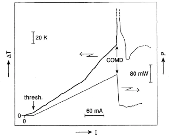
In the CW study of the time evolution of devices as a function of the driving current, it became apparent [10] that the onset of the rapid non-linear temperature rise characteristic of COD is launched at approximately the same facet temperature range, regardless of the current level. This range has been measured using different techniques. Micro-Raman (µR) spectroscopy studies on AlGaAs QW diodes have typically estimated critical facet temperatures of ~120-180 oC [10,11]. Much higher temperatures (∆T ~ 400-800 K) have been reported from Raman signals recorded while the laser undergoes COD [10,12], see Figure 1. Thermoreflectance measurements on AlGaAs laser diodes on their route to COD were also carried out [13]; as shown in Figure 2, a critical temperature ∆T ≈ 120±10 K was measured, and it was found to be practically independent of the surface treatment and coating. As the critical temperature was reached, the devices rapidly switched into a COD-like regime, and ∆T reached ≈330 K within approximately 2 s. If compared with
µR, reflectance modulation involves substantially shorter measuring times, which render it more appropriate for the study of COD kinetics. This high speed also permits to record facet temperature maps [14].
of studies [18,19] on the kinetics of COD based on this parameter are, at least, questionable.
An altogether different approach for the direct determination of the facet temperature was adopted by Sweeney et al. [20]. They studied high-power 980-nm strained QW laser diodes by measuring the very high energy Boltzmann tail (1.52-1.58 eV) of the laser emission. As a result of the larger absorption coefficients in the laser cavity for those high energy photons, the light detected would only be sourced from a region very close to the facet. This technique has the inconvenient of being very time consuming (about 1 hour per measurement). Under CW operation the tested devices underwent thermal rollover due to Joule heating, and COD was not observed. Under a CW current of 500 mA they measured facet temperatures of about 170 oC. However, they did detect COD under pulsed high power operation (500-ns long pulses at a 10 kHz repetition rate). Self-heating is very significantly reduced in the pulsed mode, and high power operating levels could be achieved. Facet temperatures of about 400±100 oC were estimated at 500 mA, which rose to about 1000 oC at 1000 mA. If the current was further increased, COD was launched.
Despite not being adequate for the precise determination of the critical temperature launching the COD, thermal infrared imaging (TII) [21–26] and time-resolved electroluminescence (TR-EL) [27–30] have been used to monitor the degradation of laser diodes under progressively increasing bias currents [21,31], pulsed high power operation [22,23,25,26], and CW accelerated [27,29,32] or low-stress [26,30,33] lifetests.
Some relevant aspects of COD have been clarified with these techniques. In TII experiments the thermal runaway effect of COD is detected by the camera as a thermal flash [22,31]. This event has been demonstrated to be an extremely fast (hundreds of ns) [34] and spatially confined effect [21]. The temperatures at the facet just prior to COD and at the hot spots as they give rise to the thermal flashes were indirectly estimated. A critical facet temperature of ~160 oC was derived [35], in good agreement with the figures reported from microRaman and TR. Regarding the hot spot, the peak temperature was determined to be close to the melting point of the QW constituent material [36]. Experimental facts indicate that COD first destroys the QW; this is shortly afterwards (~ 1ns) followed by the amorphization of part of the waveguide [25]. Furthermore, in long-term aging tests, the activation of the sudden degradation mechanism that launches COD was related to the progressive accumulation of defects in the active region of the laser diodes [26].
signature for COD were undertaken, and though the tests could be stopped for a few specimens before they showed a significant drop in the optical power output, no clear signs of extended defects were observed [29].
2.2. Post-COD analysis
Long term COD is a sudden phenomenon, which makes it very difficult to catch in real time. This means that most of the information about the COD process is obtained by post-mortem analysis of failed devices. The crystallographic fingerprint of the COD is the dark line defect (DLD), which is an elongated defect, aligned with the laser cavity, that gives a dark contrast in luminescence images, e.g., cathodoluminescence (CL) [37], and electroluminescence (EL) [32].
One needs to unravel the characteristics of the defects in order to understand the successive steps of the degradation. For this purpose, microscopic and analytical techniques are necessary. Among the observation techniques of failed devices, CL [37] and electron beam induced currents (EBIC) [23,38]are very useful because they provide a high resolution full image of the damaged zone of the failed laser. CL images of lasers after COD show the DLDs following the optical field instead of a specific crystallographic direction. The DLDs can start at the mirror facets, or inside the laser cavity. The propagation along the cavity is assisted by the reabsorption of the laser radiation due to the bandgap shrinkage at local hot spots in the active zone of the laser. Figure 4 shows CL and EBIC images of two InGaAs/AlGaAs lasers: a narrow stripe single mode laser, and broad emitter multimode laser. In the case of the narrow stripe laser the DLD is fully aligned along the cavity axis, while in the broad emitter one observes DLDs tilted with respect to the cavity axis, which are associated with circulating ring modes, characteristic of broad emitter lasers [39]. These defect patterns outline the role played by the optical field in the propagation of the defects. The spectral analysis by CL reveals that the DLDs mainly concern the QW. However, the guide layers can be also damaged in certain regions. As observed in the monochromatic CL images of a degraded single mode stripe laser, besides the DLD aligned along the cavity, the QW exhibits transverse DLDs aligned along the <1-10> crystal axis, what we call crystallographic DLDs. These crystallographic DLDs are not observed in the guide layer, as shown in Figure 5. It should be noted that DLDs are observed independently of the aging procedure followed to induce the COD, either an electrostatic discharge (ESD), pulsed current aging, or long term CW aging. Transmission electron microscopy (TEM) analyses of failed devices show local QW melting, networks of dislocations, and chemical composition changes in the COD damaged regions of the active zone of the lasers, both the QW and the guiding layers; the damage, however, does not extend to the cladding and contact layers. Note that, contrarily to previous observations [40], the DLDs do not necessarily involve melting of the active layer.
similar. Hence, one cannot establish that the weak points of the laser failing under high power pulses would correspond to the weak points in long term COD aging.
Taking account of these experimental observations, one can set-up a COD degradation scenario, which shall be developed in detail later on. To put it briefly, COD starts at a tiny heat source inside the QW; this heat source is fuelled by the laser radiation absorption, with the concomitant temperature increase; in turn, the local heating would produce thermal stresses that will eventually lead to the fatal COD outcome.
3. Physical models for COD
In this section, various models that have been devised for the description of COD will be scrutinised. The conclusions derived from mathematical computations performed on these models will be discussed. We will focus on conventional DH and QW edge emitter laser diodes, so that vertical-cavity surface-emitting lasers (VCSELs) and quantum cascade lasers (QCLs) will lay outside of our scope.
The development of physical-mathematical simulations for the interpretation and replication of the mechanisms involved in COD can be traced back to the early seventies, when Eliseev [41] proposed a simple model for the degradation of GaAs DH lasers. In that paper, which also dealt with the gradual degradation and the aging kinetics of laser diodes, a model for laser self-damage under a strong optical flux density was brought forward. This model assumed an initial local temperature inhomogeneity. The higher temperature in this much localised zone within the active layer of the device leads to an increased absorption of the laser radiation generated in the rest of the cavity, which remains cold. The absorption coefficient variation was characterised by a square root temperature dependence:
𝛼𝛼(𝑇𝑇) =𝛼𝛼0[(𝑇𝑇 − 𝑇𝑇1)/𝑇𝑇0]1/2 = 103𝑐𝑐𝑐𝑐−1𝐾𝐾−1/2(𝑇𝑇 − 𝑇𝑇1)1/2
where T1 is an initial average temperature in the active region, and α0 and T0 are parameters fitted to GaAs characteristics [9,41]. The subsequent heating of that region would eventually lead to a thermal runaway process. Therefore, the bases of most of the forthcoming physical models for COD were already set up at this early stage. The problem was analysed from a simplified one-dimensional perspective, and it was concluded that the optical flux density derived from experimental measurements was not high enough to cause the melting or the decomposition of the active layer. The thermoelastic stress in the proximity of the heated areas was proposed as the most probable source of the facet damage. This line of thought did not have an impact on future works and was apparently abandoned.
recombination of excess carriers. In other articles, the contribution of ohmic heating, either solely at the contacts[44] or encompassing all the layers across the structure[45,46], as well as the reabsorption of the spontaneous and stimulated radiation[44–46], were also reflected. In any case, although current spreading effects were occasionally considered[45,46], in general these heat sources were evenly distributed in each one of the layers and, therefore, the models are not suitable for the description of the physical phenomena leading to a local event such as COD.
Hence, this particular area of research remained relatively inactive until the end of the decade, when another model for COD in AlGaAs DH lasers was developed by Henry and co-workers [4]. Their experimental study departed markedly from the normal operation of a DL, as pulsed laser light from an Ar laser was focused on the active layer of the DH structure in order to generate carriers in a localised spot. The recombination of the photogenerated carriers in that limited zone produced a superradiant (SR) light confined to the active layer of the structure, that caused local melting and formation of dark lines. The calculations of the local heating in the structure specifically considered a temperature-dependent absorption reportedly derived from experimental data [47,48]. However, doubts have been raised about the choice for the initial optical absorption parameter prior to the heating effect[9], as it may lead to an excessive power dissipation at the initial stages of the degradation. The model also explicitly considered the rate of non-radiative recombination at the surface in order to estimate whether the process was fast enough to allow for the melting point to be reached under pulsed operation mode. Though this was a novel and relevant concept, the assumed carrier distribution close to the heated spot has also been questioned [9]. The complicated thermal simulation was simplified by considering a one-dimensional heat flow away from the surface, and assuming that the initial absorption coefficient α0=140 cm-1 upon heating increases exponentially with temperature as
Δ𝛼𝛼=𝛼𝛼0 [exp(𝛥𝛥𝑇𝑇/21.4 𝑜𝑜𝐶𝐶)−1].
A constant thermal conductivity (k=0.19 W/cm·K, fitting for Al0.08Ga0.92As at about 60 oC) was used throughout. Additionally, a 0.4 µm thick layer was assumed to absorb light
at the start of the process, while the increase of the absorption coefficient was limited to a layer 0.2 µm thick; moreover, the total absorbed power was limited to two-thirds of the incident flux light, though no justifications were given for these particular choices. The results from this model are illustrated in Figure 6: at the beginning, the curve corresponds to 0.74% of the light flux being absorbed, whereas in the last stage two-thirds of the flux are absorbed. The switching between the two absorption regimes would correspond to the thermal runaway process. Comparison with the experimental data reported in the same work showed a reasonable agreement in the computed solutions. Regardless of its possible shortcomings, the work by Henry et al. steered interest in the field and several publications with further developments followed shortly [31].
half-space, so that the structure of the device had to be neglected. The model allowed to determine the heat flux that would lead to that critical temperature rise as a function of the pulse width used for laser operation. In particular, for CW operation, the model derived an expression for the maximum flux qmax that could be expressed as:
𝑞𝑞𝑚𝑚𝑚𝑚𝑚𝑚 = 𝜋𝜋𝑇𝑇0𝐾𝐾0/2 [𝑏𝑏𝐾𝐾(𝑐𝑐)]−1ln(1 +Δ𝑇𝑇𝑚𝑚𝑚𝑚𝑚𝑚/𝑇𝑇0)
were K(m) is the complete elliptic integral of the first kind, with m = 1 – (b/a)2. For an operation temperature of 300 K, a maximum heat flux of 1.6·106 W/cm2 was derived. Though, as stated above, the dimensions of the heat source were considered, a and b were fixed for the calculations, and the possible influence of the size of the heated region on the triggering of COD was not studied.
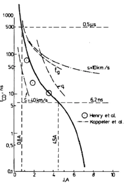
Nakwaski[50] extended the work by Henry et al [31]. While accepting the same assumptions about the heat generation at the surface of the DH laser, explicit temperature dependences were considered for the thermal conductivity and diffusivity. Moreover, the heat generated in the volume of the active layer was added to the scheme and shown to be relevant at the first stage of the process. In order to simplify the formulation of the problem, the Kirchhoff transformation was applied in order to consider the temperature dependence of the thermal conductivity. Furthermore, a space transformation was used to substitute the GaAs/AlGaAs heterostructure by a homogeneous AlGaAs homostructure. This can be done as long as nearly all the heat is spread in the active AlGaAs layer, so that the derived expressions may be correct only for t<<0.5 µs. These two transformations lead to a linear and much simpler thermal conduction equation. This equation was solved using the method of Green’s functions and, after imposing the necessary boundary and initial conditions, the time-dependent temperature profiles for the laser were computed. A comparison between the results for catastrophic degradation times vs. amplitude of the pulses as derived from the models by Henry et al. [31], Kappeler et al. [34] and Nakwaski [35], is shown in Figure 7.
Nakwaski later undertook the case of high power operation [51,52] in DH lasers, and refined the expression for the temperature dependence of the absorption coefficient. Based on considerations regarding the absorption coefficient, and in line with Henry and co-workers’ treatment of that parameter, both this and the previous model considered that COD was triggered when a 21.4 K temperature increase was reached at the surface of the laser. A time-dependent effective thermal diffusivity was incorporated in the mathematical modeling, whereas volume heat sources were excluded, so that only the power dissipation around the catastrophically damaged area was considered. This article also marks the first occasion on which the influence of the facet reflectivities on COD was tackled and numerically determined.
the removal of heat from the active area to the heat sink, an ad hoc effective thermal resistance length parameter (H) was introduced. The heat equation included two sources for the generation of heat, namely, the non-radiative recombination throughout the active region, and Joule heating at the ohmic contact. The Joule heating was supposed to affect the net gain in a different fashion than the temperature increase due to the recombination of carriers, though the authors readily abandoned this approach [54]. An expression was derived for the total temperature rise at the surface of the laser, and the results were compared to experimental data for an AlGaAs device. The authors argued that as the laser operated continuously, the facet would progressively deteriorate. This would result in an increasing surface recombination velocity, and surface temperature would rise with time, but in a manner they could not devise, so that this effect was not included in their model.
The same group published shortly afterwards [54] an article focusing on hypothetical conditions for no thermal runaway in CW lasers. This time they followed a strictly time-dependent approach by modifying their previous carrier diffusion and heat conservation equations. Joule heating was excluded, thus the only heat source was due to non-radiative recombination at the facet, as introduced in the boundary conditions for the heat equation. Hence, extended heating was substituted by a planar heat source on the facet of the laser. By solving the equation, they arrived at a criterion that, according to the authors, could be used to systematically optimize laser structures.
A final paper was published pursuing the same goal [55]. This time a two-dimensional framework was used by modifying the expressions from the previous paper accordingly. A further refinement was introduced by explicitly considering the heat transfer from the device to the surrounding gas in its environment. The study concluded that the output from a laser could be increased by reducing the stripe width, a result that notably disagrees with the common knowledge for high power lasers [9].
scheme was used to study the effect of unpumped facet regions. The work concluded that an improved COD power level could be achieved if factors such as the width and thickness of the unpumped region, reflectivities at the facets and the series resistances of the claddings were carefully optimised.
As the fabrication of high power lasers switched from DH to QW devices, so did the physical models. Fujii et al. [58] relied on Henry’s assumptions to perform calculations that quantitatively explained the experimentally observed differences between the COD power densities for AlGaAs and AlGaInP QW laser diodes. They concluded that the higher thermal resistivity of AlGaInP, when compared to AlGaAs, determined the lower COD levels for the first device, COD power densities being roughly inversely proportional to the square root of the thermal resistivities.
Chen and Tien [16] worked within a framework similar to that of Schatz and Bethea, solving a three-dimensional heat equation, whereas the heat generation mechanisms were described through a one-dimensional carrier diffusion equation. Certain points in their description of COD for QW lasers are worth being mentioned. First, when comparing their results with those derived from experimental data, they pointed out to the differences between the values measured with typical probe beams of around 1-1.5 µm, and local maximum temperatures in QW devices. Second, they observed that the corrected experimental temperature increments were about 5 times larger than those computed, so that size effects [59] on the thermal conductivities of the thinner layers were invoked. When these were considered, the correlation was notably improved. The authors foresaw that solving the Boltzmann transport equation (rather than the heat equation) and establishing a more precise description of the thermal conductivities of the active layers by explicitly including their anisotropic character [59], would yield a more accurate picture of the heating of the laser. Finally, the interpretation of the feedback mechanism eventually leading to COD departed from the previously accepted model for DH lasers. According to all the models so far cited, a temperature-induced band gap shrinkage in the heated region shifts the absorption spectrum to a lower frequency and, in turn, prompts an increased absorption of the laser light and further heating of the facet that eventually leads to melting. Chen and Tien argued that a decrease of the absorption should follow in the case of a QW and proposed an alternative path via temperature enhanced absorption in the cladding layers of the laser structure. The authors must have been invoking the excitonic characteristics of QW absorption as the factor leading to that reduction. However, for free carriers in excess of 1017 cm-3, screening effects modify notably the absorption spectra of QWs [60] and the excitonic structure vanishes.
Eliseev [9] proposed a self-consistent scheme for facet heating. This model derived the temperature, carrier concentration and, additionally, current profiles in the laser. It aimed at considering current redistribution induced by enhanced carrier consumption near the surface, as well as local temperature dependent bandgap shrinkage. The predicted temperature rise was lower than the experimentally determined values, so that it failed to describe the thermal runaway process. The author claimed that, under strong action of current crowding and optical reabsorption, the increase in the temperature would be higher than the measured threshold for COD and sufficiently large for the waveguide region to start absorbing the laser radiation.
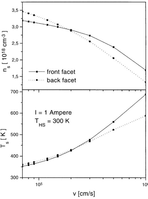
an initial study on the temperature dependence of several factors that determine the operational characteristics of QW lasers [61]. In this article, they also evaluated the relative weight of different recombination mechanisms (stimulated emission, spontaneous emission, Auger recombination, leakage current, interface recombination) on the loss process as a function of the operating temperature. This was the basis for a study [62] on thermal dissipation in QW lasers that was formulated in a 2D scheme and numerically solved using FEM. The paper basically followed the same path as previous studies by Manning [44] and Sarzala and Nakwaski [45], though this work was further supported by a comparison of the computed solutions with those derived from an analytical resolution of the equations that describe the problem. The model was later modified [63] in order to allow for a significant fraction of the heat loss to be dissipated in the vicinity of the facets. By doing so, the thermal conditions prior to launching the COD could be replicated. By comparing the computed results with experimental µR data, it was concluded that up to 7% of the total heat power is located at the front facet. The need for the enhanced heat dissipation close to the facets had been previously anticipated when attempting to use the original model for the description of the aging process in QW lasers [64]. Eventually, Menzel [65] reported a self-consistent method for the calculation of the photon density, the carrier density and the temperature profiles as a function of time in a 1D framework. A relaxation method was used to solve for the system of coupled non-linear differential equations. The resonator was divided into 200 elements that were more closely spaced in the vicinity of the facets, in order to take account of the stronger recombination and the more accused temperature variations in those regions. Figure 8 illustrates the changes of the facet temperatures Ts and the carrier densities at the front and back facets as a function of the surface recombination velocity. This work described COD under CW operation as a result of long-term facet degradation that yields to increased surface recombination velocities.
Smith [66] followed a similar approach to that of Menzel’s. Through an elaborate mathematical description, the coupling of electrical, optical and thermal effects is described in one-dimensional space. The set of coupled differential equations was reduced to a single second-order boundary value problem via a systematic asymptotic expansion. The conditions leading to thermal runaway were analysed and correlated with the density of defects in the vicinity of the surface, as well as the extension of that defect-rich region. Sudden failure was rationalised in terms of the progressive deterioration of devices for which the initial concentrations of defects lead to steady state solutions; the aging of the laser leads to an increase in the concentration of defects, and, as the threshold determined by the model is crossed, the thermal runaway is launched.
in the value of the thermal conductivity of the thinner layers and opted for what is termed as a worst case scenario by assuming one-tenth of the bulk value for the active layers of the laser.
The discrepancies between 3D and lower dimensional thermal modeling were also inspected by Mukherjee and McInerney [68]. Their approach did not include optical rate equations, but similar conclusions to those derived by Romo et al. were reached. Current spreading and facet heating are only properly described in a 3D scheme, and the progressive deviation of the 2D from the 3D model as the injection current increases is demonstrated. This work also inspected the effect that the inhomogeneous temperature distributions would play in determining the lateral mode structure, a relevant factor for the operation of high-power broad-area laser diodes.
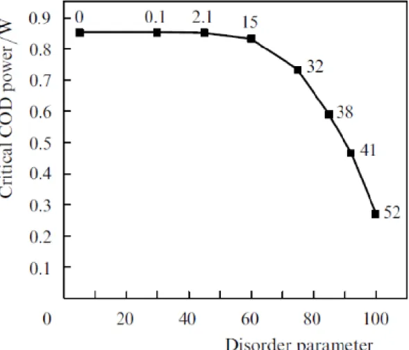
On the last model that will be reviewed here, Miftakhutdinov and co-workers [69,70] also undertook a self-consistent electro-opto-thermal description of the problem. The structure of the device was refined by considering the effect of the facet coating materials; the thermal behaviour of the laser itself was described in terms of a single thermal conductivity for the layered structure. Up to six distinct thermal sources were considered, with emphasis placed on the heating processes in a degraded region next to the facet and on optical absorption in the heated cladding layers (see above [16]). 3D and 1D schemes were adopted for the thermal and laser problems, respectively. When compared to other works, the 1D approach is upgraded, as the Gaussian 2D photon profile (and 1D carrier profile) in the plane orthogonal to the propagation of the laser beam was specifically considered in the active layer. In order to achieve the global convergence of the discretized problem, the same flow algorithm detailed above in Romo and co-workers’ approach was basically followed. The calculations showed that the temperature increase depended markedly on the size of the degraded region, as well as on a disorder parameter (see Figure 9) that is introduced in order to describe fluctuations of the crystal potential, which can have either a dynamic (phonons) or static (impurities, defects) origins. Therefore, high concentrations of defects would facilitate the onset of COD.
4. Physical properties on the nanoscale
4.1. Thermal conductivity
In parallel with the progressive reduction of the size of electronic and electro-optic devices, nanoscale heat transport has been the subject of an increasing interest. Extensive reviews focusing on experimental techniques and results for a wide variety of systems, as well as on physical models specifically devised for low-dimensional structures, have been published in recent years [74,75]. Generally speaking, when the characteristic size of a structure (or of a layer within a structure) becomes comparable to or smaller than the mean free path of the phonons, the thermal properties depart from those of the bulk. The classical theories for lattice thermal conductivity of Callaway [76] and Holland [77] cannot straightforwardly describe the behaviour of these low-dimensionality systems. Furthermore, the applicability of the Fourier law under these conditions is, to say the least, debatable. Even the description of these systems in terms of the temperature is not without its issues [74]: the statistical definition of temperature in connection with the average energy of a set of particles, is difficult to transpose, e.g., to a QW with a layer thickness of about 10 nm. However, in practice, the Fourier theory has often been applied to nanostructures by using a structural-dependent thermal conductivity [78].
III-V semiconductor superlattices (SLs) have been widely used in optoelectronics, e.g., in quantum cascade lasers (QCLs) and vertical-cavity surface-emitting lasers (VCSELs). In our case, the similarity of these structures to those in the central layers of QW laser diodes will give some indirect hints about the effective thermal conductivities in the active region of the lasers.
Several experimental techniques have been applied in order to measure the thermal properties of AlAs/GaAs superlattices. Yao [79] used an ac calorimetric method based on that of Hatta and co-workers [80] to determine the thermal conductivity and diffusivity of SLs grown by MBE with identical thicknesses of the repeated AlAs and GaAs constituting layers, that ranged from 5 to 50 nm. Under the experimental configuration, the heat flew along the layers. Yao found that both thermal properties were lower than those of bulk AlAs and GaAs, but larger than the corresponding figures for the Al0.5Ga0.5As alloy, a fact that he attributed to the suppression of alloy scattering in the superlattice. He also observed that as the superlattice period diminished, the thermal conductivity and diffusivity also decreased and approached the values of the alloy for the shortest periods.
Chen et al. [81] measured the thermal diffusivity for the Bragg reflectors of a VCSEL both in the parallel and the perpendicular directions to the AlAs and GaAs layers. The method specified above [79] was also used for the measurement of the parallel diffusivity, whereas a thin film resistive temperature sensor was directly patterned onto the samples to overcome the difficulties derived from the short heat diffusion time across the films. The results showed that the diffusivities of the VCSEL structures were about 5-7 times lower than those of bulk structures. Furthermore, an anisotropy was observed when the data for the parallel and the perpendicular directions to the growth plane were compared.
for most of the temperature range considered, a large reduction in the thermal conductivity, when compared to the bulk counterpart, was measured (40% smaller at room temperature). This was rationalised in terms of interface scattering effects. Similar conclusions were reached by Piprek et al. [83], who recorded about 50% thermal conductivity reduction compared to the average bulk value for measurements performed at room temperature on a 115 nm/134 nm GaAs/AlAs periodic structure. The experimental setups for both this and the previously cited work were based on Hatta and co-workers’ ac calorimetric method [80].
A pump-and-probe time-domain thermoreflectance (TDTR) technique [84] was used by Capinski et al. [85] to measure thermal conductivity in the direction normal to the interfaces of (AlAs)n/(GaAs)n superlattices in the temperature range from 100 to 375 K, with the number of monolayers (n) ranging from 1 to 40. The superlattice period varied from 10 (for n=40) to 800 (for n=1), so that the global thickness of the superlattices was in the 200-850 nm range. The thermal conductivity decreases monotonically as the number of monolayers is reduced, although some deviations from that global trend are observed. At room temperature and for n=40, the measured conductivity is approximately one-third of the bulk value, while for n=1 it is an order of magnitude less than that of the bulk. When the temperature dependence is analysed, the reduction of the thermal conductivity is more accused as the temperature is decreased.
Luckyanova et al. [86] measured the thermal conductivity of 2 nm/2 nm and 8 nm/8 nm GaAs/AlAs SLs for both cross-plane and in-plane directions at 296 K. As in the above cited work, the TDTR technique was used to determine the cross-plane conductivity, whereas a transient thermal grating (TTG) technique measured the in-plane thermal conductivity. The cross-plane values were approximately one fifth (8 nm) and one-seventh (2 nm) of the bulk figure. The in-plane thermal conductivities were larger than the cross-plane counterparts by a factor of 1.2~1.3. The measured values were compared to first principle calculations of the thermal conductivities using density functional perturbation theory (DFPT), which yielded a reasonable agreement with the measured anisotropy of the conductivity, whereas the predicted values were more than twice the measured figures.
A summary of the reported thermal conductivities of GaAs/AlAs SLs from the works so far cited is shown in Figure 10, from which a good correlation between the measurements performed with the different experimental techniques is derived. A clear reduction of the thermal conductivity as the layer thickness diminishes is detected, and a certain degree of anisotropy is also observed. Therefore, a similar behaviour should also be expected for the nanometre range layers that form the active parts of laser diodes. A number of theoretical works have focused on the size dependence of the thermal conductivity for thin film-quantum well structures [59,87,88]. All of them infer a marked reduction for this parameter as the thickness diminishes. Both Balandin and Wang [87] and Liang and Li [88] predicted a decrease of the lattice thermal conductivity by an order of magnitude as the dimension of the layer falls into the ~10 nm range.
which is the case for the systems we are considering here. The epitaxial growth with state-of-the-art technology permits to fabricate layers of excellent crystalline quality; the layers forming the laser diodes can be considered dislocation free. Therefore, if the fingerprint of the degradation is the generation of dislocations, it should result in an additional reduction of the thermal conductivity.
4.2. Mechanical strength
Outstanding departures of the mechanical properties of nanostructures, when compared to their bulk counterparts, have been reported for different systems and configurations [95,96]. Remarkably high sub-micron yield strengths have been explained in terms of different mechanisms [97–99] that establish diverse connections between this mechanical parameter and the characteristic lowest dimension (h) of the systems. If we focus on the most widely invoked approach, the Hall-Petch model [97,100,101] estimates an h-1/2 dependence for the yield strength, whereas a ln(h)/h relationship is predicted by the modified confined layer slip (CLS) model [98,99].
Metals have been the subject of a large number of research papers on these size-dependent ultra-strength phenomena, but the amount of experimental evidence of these effects on semiconductors is comparatively scarce. Gerberich and co-workers [102] analysed the available information for silicon nanopillars, nanowires, and nanospheres, and showed that the strength, ductility and toughness of these systems increase with the inverse radius of the applicable reduced dimension.
The groups of Profs. Mai and Jagadish, from the University of Sidney and the Australian National University, respectively, have jointly undertaken a series of investigations on the mechanical properties of GaAs nanowires during the present decade [108–112]. The first paper [108] reports on compression tests conducted on GaAs nanowires with diameters ranging from 9 – 160 nm. They used a commercial Hysitron PI 95 TEM PicoIndenter with a diamond flat punch under a constant displacement mode and recorded the corresponding displacement-force-time curves. The interpretation of the curves was not straightforward given the fact that the nanowires bent under the applied forces, and therefore finite element analysis was performed in order to extract the relevant information, namely, the failure strain and the Young modulus. The calculated Young modulus for the thicker (diameter larger than 100 nm) nanowires is about 118 GPa, which is roughly equivalent to that of bulk GaAs along the [1 1 1] stacking direction. As the diameter decreases to 65-55 nm, the Young modulus increases to approximately 190 GPa. These figures were later confirmed with mechanical resonance tests [112]. However, the strong size effect for diameters <100 nm has been related to the amorphous oxide shell[111] on the nanowire, and, as such, it would not be a property of the GaAs system. The failure strain remains almost constant at 0.10-0.11 throughout the 50-160 nm diameter range, so that a yield stress of approximately 12 GPa can be estimated. This value is almost an order of magnitude larger than the bulk figure. This information should, however, be treated with care, as the authors state that for the smaller diameters the nanowires clearly underwent a combined elastic and plastic deformation [108]. Hence, the reported failure strain may exceed the yield strain, so that the yield stress is probably overestimated.
Even though all the experimental evidence on yield strength enhancement of the GaAs system has been derived for cylindrical structures, the results can be readily extrapolated to thin film configurations. As shown by Jennet et al. [113], the yield stress in nanostructures is determined by the smallest dimension, the other dimensions making little or no difference, so that nanolayers would be as strong as nanowires and nanoparticles.
It is also worth mentioning that a few studies have been published on the plastic deformation of GaAs/AlAs SLs. Micro- [114,115] and nanoindentation [116] were used to investigate the behaviour of the SLs. However, the very nature of these tests, in which the systems are driven beyond the elastic limits, and for which the penetration depth of the indenters by far exceed the characteristic dimensions of the individual layers, preclude the extraction of any significant information for our present purposes.
5. The incidence of nanoscale effects on COD
The model, like others described in section 3 [65–70], relies on finite element methods for the mathematical computations. From the very beginning, we opted for a three-dimensional picture of AlGaAs devices, in which the specific and temperature dependent properties of the individual layers, both those with a fixed composition and the cladding layers with a gradual change in the Al content, were considered. Unlike other more elaborated pictures that have attempted a self-consistent opto-electro-thermal statement and resolution of the problem, our approach basically assumes that, as a result of the non-radiative recombination processes and the self-absorption of laser photons, a heat source is localized over a small region of the mirror facet, though it can be easily extended to a localized heat source inside the laser cavity.
The model was originally devised to elucidate the role of the thermal stresses on the generation of dislocations and the formation of V-defects in laser bars [117], but the focus rapidly switched to the consideration of COD as a phenomenon triggered as the thermal stresses overcome the yield strength of the materials [118,119]. Within this framework, as the plastic deformation limit is attained, dislocations are formed and they propagate driven by the laser field. The dislocations induce enhancements of the non-radiative recombination rate and light self-absorption.
The mathematical simulations lead to temperature and stress profiles in the structure which are computed for different power densities, which correspond to the part of the absorbed laser radiation converted into heat at the local heat source. Pairs of maximum temperature-maximum stress data were compared to experimental yield strengths of GaAs, and the crossing of the two curves was identified as the onset of COD. As depicted in Figure 11, our initial guesses estimated that thermal stresses by themselves would overcome the yield strength at around 500 K [118], close to the critical temperatures commonly reported for the starting of the thermal runaway (120 – 180 oC).As shown in Figure 11, if the packaging induced stress present in laser bars (which is also compressive) is considered the temperature for the onset is about 460 K. Qiao et al. have followed the same approach and reported similar results when analysing the effects of lateral spatial hole burning on the degradation of broad-area AlGaAs/GaAs laser diodes [85]. The computer simulated thermal stresses were compared to x-ray diffraction post-COD results, and they suggested that the laser underwent plastic deformation during the degradation process.
the physical probes used for the measurements were explicitly considered [17] (~ 1 µm diameter laser beam spot for µR or thermoreflectance, ~4 µm lateral pixel size for thermocameras). It was inferred that experimental techniques yield average rather than local critical temperatures, as previously pointed out by Chen and Tien [16]. However, the average temperature estimates for the onset of COD as derived from our model proved too low when confronted with the reported data for a QW laser diode, whereas the model worked reasonably well for a DH laser [109].
The fact that the model was adequate for a DH device with a 200 nm thick GaAs active layer, but not for the 12 nm thick QW, was an indication that our approach was not fully correct. As the size-dependent thermal conductivity effects had already been considered, the enhancement of the mechanical strength and the corresponding displacement of the onset of plasticity for the thinnest layers were brought into the scheme [124]. In want for more detailed experimental studies, the available yield strength data for low dimensional structures [104,107] were extrapolated in order to simulate the mechanical behaviour of the guide layers and the QW. The displacement of the corresponding yield stress curves, which is displayed in Figure 12, leads to a reassessment of the temperature at which yield is produced in the laser, that was then estimated to be around 600-630 K. The computed average temperature derived from those values results in a better agreement with the reported critical temperatures for COD in QW laser diodes.
Now, let us look at the path leading to COD. According to our interpretation, it differs depending on whether the diode is being operated at very high power-short pulse or at CW conditions. In the first case, we would be considering an instantaneously generated COD, while the second would correspond to a long term aging prior to COD. The instantaneous COD would be caused by very intense current pulses, which would readily give rise to heat sources which are intense enough to overcome the yield stress locally. For a laser diode working for a long period of time under CW conditions, the generation of heat in the QW is due to the non-radiative recombination at point defects, Joule heating induced by local resistance reduction and, as the temperature is locally enhanced, reabsorption of the laser light, which feeds the non-radiative recombination. As a result of the sustained operation of the laser, further point defects and/or microprecipitates are generated; therefore, the generated heat gradually increases for a given operating voltage, and, concomitantly, higher local temperatures are reached in the QW. An approximately linear relationship between the power density at the local heat source and the peak temperature in the QW is derived from our model. The critical temperature would be eventually reached in the defect-richest zone of the active layer.
From that point on, both pulsed and CW COD would experiment the same outcomes. Dislocations would be generated, giving rise to a two-fold effect. On the one hand, they notably affect the absorption coefficient [125], so that the laser light reabsorption would be enhanced. On the other hand, dislocations produce a further drop in the thermal conductivity [90,92]. This gives rise to a drastic superlinear temperature rise that leads to the sudden degradation, which is characteristic of the thermal runaway. The scheme of the whole process is shown in Figure 13.
poor power dissipation under these conditions as the fundamental cause leading to COD [126]. If the additional degradation of the thermal conductivity is not considered, the increased laser light absorption that is commonly cited as the main feedback effect launching the COD, is not sufficient to get to the melting point in the QW, and a saturation regime [56] would be reached. As cited before, a somewhat similar conclusion was drawn by Eliseev [9], who claimed that a strong action of current crowding and optical reabsorption would be needed to reach the final stage of COD, though he did not propose any mechanisms inducing such outcomes. The path to COD is summarised in Figure 14, were the paramount role played by the extrinsic loop activated by the extended generation of dislocations on laser reabsorption and, more importantly, on the decrease of the thermal conductivity in the active layers, is highlighted.
6. Conclusions
In spite of the considerable volume of studies on the catastrophic degradation mode of laser diodes, some aspects of COD remain poorly characterised. Real-time examination remains a challenging task due to the fast kinetics of the process, which renders all the experimental techniques so far developed for this purpose insufficient for a clear identification of the specific mechanisms that launch the feedback process. On the other hand, post-mortem examination makes it difficult to elucidate whether certain features of the modified structures or altered physical properties are root causes of COD or merely its by-products. Most of the interpretations so far proposed consider structural damages, such as dark bands and V-defects, as collateral effects taking place during the last stage of COD. However, the progressive accumulation of defects, which obviously results in modifications of the structure, has been clearly identified as a factor influencing the degradation process. The onset of plastic deformation in the active region of the laser diodes is proposed as a plausible mechanism for initiating the thermal runaway.
Physical models based on sound assumptions derived from the experimental data have aided in establishing feasible degradation paths leading to COD. Nanoscale effects on thermal conductivity have been occasionally considered in some of those models. This physical property effectively determines how the heat generated in the active region is dissipated, it determines how much energy is concentrated in the heat source, and therefore should play a key role in the degradation path scheme. However, this is not the only property which is affected by the reduced dimensions of the active layers forming the laser. The changes in the mechanical strength should also be considered in laser structures based on QWs. The incorporation of these two size-dependent effects results in an alternative model in which the deterioration of the thermal conductivity due to plastic deformation of the QW plays a paramount role.
Acknowledgments
This work was funded by Junta de Castilla y León (Projects VA081U16 and VA283P18), and Spanish Government (ENE 2014-56069-C4-4-R and ENE 2017-89561-C4-3-R). J L Pura was granted by the FPU programme (Spanish Government) (FPU14/00916).
References
[1] Neukum J 2008 Innovation enriches high power diode laser market Opt. Laser Eur. 165 37–9
[2] Tomm J W and Jiménez J 2007 Quantum-Well Laser Array Packaging (New York: McGraw-Hill)
[3] Hakki B W and Nash F R 1974 Catastrophic failure in GaAs double-heterostructure injection lasers J. Appl. Phys. 45 3907–12
[4] Henry C H, Petroff P M, Logan R A and Merritt F R 1979 Catastrophic damage of AlxGa1-xAs double-heterostructure laser material J. Appl. Phys. 50 3721–32 [5] Fukuda M 1991 Reliability and Degradation of Semiconductors Lasers and LEDs
(Boston: Artech House)
[6] Ueda O 2010 On Degradation Studies of III–V Compound Semiconductor Optical Devices over Three Decades: Focusing on Gradual Degradation Jpn. J. Appl. Phys.
49 090001
[7] Tomm J W, Ziegler M, Hempel M and Elsaesser T 2011 Mechanisms and fast kinetics of the catastrophic optical damage (COD) in GaAs-based diode lasers
Laser Photon. Rev. 5 422–41
[8] Epperlein P W 2013 Semiconductor Laser Engineering, Reliability and Diagnostics (Oxford, UK: John Wiley & Sons Ltd)
[9] Eliseev P G 1996 Optical strength of semiconductor laser materials Prog. Quantum Electron. 20 1–82
[10] Tang W C, Rosen H J, Vettiger P and Webb D J 1991 Raman microprobe study of the time development of AlGaAs single quantum well laser facet temperature on route to catastrophic breakdown Appl. Phys. Lett. 58 557–9
[11] Hempel M, Tomm J W, Elsaesser T and Bettiati M 2012 High single-spatial-mode pulsed power from 980 nm emitting diode lasers Appl. Phys. Lett. 101 191105 [12] Bou Sanayeh M, Brick P, Schmid W, Mayer B, Müller M, Reufer M, Streubel K,
Tomm J W and Bacher G 2007 Temperature-power dependence of catastrophic optical damage in AlGaInP laser diodes Appl. Phys. Lett. 91 041115
[14] Pierścińska D, Pierściński K, Bugajski M and Tomm J W 2007 Thermal properties of high power laser bars investigated by spatially resolved thermoreflectance spectroscopy Phys. Status Solidi Appl. Mater. Sci. 204 422–9
[15] Hayakawa T 1999 Facet temperature distribution in broad stripe high power laser diodes Appl. Phys. Lett. 75 1467–9
[16] Chen G and Tien C L 1993 Facet heating of quantum well lasers J. Appl. Phys. 74 2167–74
[17] Souto J, Pura J L and Jiménez J 2016 About the physical meaning of the critical temperature for catastrophic optical damage in high power quantum well laser diodes Laser Phys. Lett. 13 025005
[18] Moser A, Latta E E and Webb D J 1989 Thermodynamics approach to catastrophic optical mirror damage of AlGaAs single quantum well lasers Appl. Phys. Lett. 55 1152–4
[19] Moser A and Latta E E 1992 Arrhenius parameters for the rate process leading to catastrophic damage of AlGaAs-GaAs laser facets J. Appl. Phys. 71 4848–53 [20] Sweeney S J, Lyons L J, Lock D and Adams A R 2002 Direct measurement of
facet temperature up to the melting point and COD in high power 980nm semiconductor diode lasers IEEE 18th Int. Semicond. Laser Conf. 9 1325–32 [21] Ziegler M, Tomm J W, Elsaesser T, Matthiesen C, Bou Sanayeh M and Brick P
2008 Real-time thermal imaging of catastrophic optical damage in red-emitting high-power diode lasers Appl. Phys. Lett. 92 2006–9
[22] Hempel M, Tomm J W, Ziegler M, Elsaesser T, Michel N and Krakowski M 2010 Catastrophic optical damage at front and rear facets of diode lasers Appl. Phys. Lett. 97 10–3
[23] Hempel M, Tomm J W, Hortelano V, Michel N, Jim J, Krakowski M and Elsaesser T 2012 Time-resolved reconstruction of defect creation sequences in diode lasers
Laser Photon. Rev. 6 L15–9
[24] Qiao Y, Feng S, Xiong C, Ma X, Zhu H, Guo C and Wei G 2012 The impact of the stress induced by lateral spatial hole burning on the degradation of broad-area AlGaAs/GaAs laser diodes J. Appl. Phys. 112 113104
[25] Hempel M, Tomm J W, Yue F, Bettiati M A and Elsaesser T 2014 Short-wavelength infrared defect emission as a probe of degradation processes in 980 nm single-mode diode lasers Laser Photon. Rev. 8 L59–64
[26] Hempel M, Tomm J W, Venables D, Rossin V, Zucker E and Elsaesser T 2015 Long-Term Aging and Quick Stress Testing of 980-nm Single-Spatial Mode Lasers J. Light. Technol. 33 4450–6
[27] Sin Y, Ives N, Presser N and Moss S C 2010 Root cause investigation of catastrophic degradation in high power multi-mode InGaAs-AlGaAs strained quantum well lasers Proceedings of SPIE vol 7583, ed M S Zediker p 758307 [28] Sin Y, Ives N, LaLumondiere S, Presser N and Moss S C 2011 Catastrophic
[29] Sin Y, LaLumondiere S D, Presser N, Foran B J, Ives N A, Lotshaw W T and Moss S C 2012 Physics of failure investigation in high-power broad-area InGaAs-AlGaAs strained quantum well lasers Proceedings of SPIE vol 8241, ed M S Zediker p 824116
[30] Sin Y, Lingley Z, Ayvazian T, Brodie M and Ives N 2018 Catastrophic Optical Bulk Damage – A New Failure Mode in High-Power InGaAs-AlGaAs Strained Quantum Well Lasers MRS Adv. 3 3329–45
[31] Qiao Y, Feng S, Xiong C, Zhu H, Ma X and Yue Y 2013 Transient thermal characteristics related to catastrophic optical damage in high power AlGaAs/GaAs laser diodes Phys. Status Solidi Appl. Mater. Sci. 210 2379–83
[32] Sin Y, Lingley Z, Presser N, Brodie M, Ives N and Moss S C 2017 Catastrophic Optical Bulk Damage in High-Power InGaAs-AlGaAs Strained Quantum Well Lasers IEEE J. Sel. Top. Quantum Electron. 23 1–13
[33] Sin Y, Presser N, Brodie M, Lingley Z, Foran B and Moss S C 2015 Degradation mechanisms in high-power multi-mode InGaAs-AlGaAs strained quantum well lasers for high-reliability applications Proceedings of SPIE vol 9348, ed M S Zediker p 93480L
[34] Elliott S N, Smowton P M, Ziegler M, Tomm J W and Zeimer U 2010 Time resolved studies of catastrophic optical mirror damage in red-emitting laser diodes
J. Appl. Phys. 107 123116
[35] Ziegler M, Tomm J W, Zeimer U and Elsaesser T 2010 Imaging catastrophic optical mirror damage in high-power diode lasers J. Electron. Mater. 39 709–14 [36] Ziegler M, Hempel M, Larsen H E, Tomm J W, Andersen P E, Clausen S, Elliott
S N and Elsaesser T 2010 Physical limits of semiconductor laser operation: A time-resolved analysis of catastrophic optical damage Appl. Phys. Lett. 97 10–3
[37] Hortelano V, Anaya J, Souto J, Jiménez J, Perinet J and Laruelle F 2013 Defect signatures in degraded high power laser diodes Microelectron. Reliab. 53 1501–5 [38] Souto J, Pura J L, Torres A, Jiménez J, Bettiati M and Laruelle F J 2016 Sequential description of the catastrophic optical damage of high power laser diodes High-Power Diode Laser Technology and Applications Xiv ed M S Zediker p 973306 [39] Chin A K, Bertaska R K, Jaspan M A, Flusberg A M, Swartz S D, Knapczyk M
T, Smilanski I and Jacob J H 2009 Catastrophic Optical-damage in High-power, Broad-area Laser-diodes MRS Proc. 1195 1195-B01-01
[40] Mahajan S, Temkin H and Logan R A 1984 Formation of optically induced catastrophic degradation lines in InGaAsP epilayers Appl. Phys. Lett. 44 119–21 [41] Eliseev P G 1973 Degradation of injection lasers J. luminiscence 7 338–56 [42] Joyce W B and Dixon R W 1975 Thermal resistance of heterostructure lasers J.
Appl. Phys. 46 855–62
[43] Kobayashi T and Iwani G 1977 Three dimensional thermal problems of double- heterostructure semiconductor lasers Jpn. J. Appl. Phys. 16 1403–8
[45] Sarzala R P and Nakwaski W 1990 An appreciation of usability of the finite element method for the thermal analysis of stripe-geometry diode lasers J. Therm. Anal. 36 1171–89
[46] Sarzala R P and Nakwaski W 1992 Thermal analysis of oside-isolated stripe diode lasers J. Therm. Anal. 38 1447–62
[47] Sell D D and Casey H C 1974 Optical absorption and photoluminescence studies of thin GaAs layers in GaAs–Al x Ga 1− x As double heterostructures J. Appl. Phys. 45 800–7
[48] Casey H C, Sell D D and Wecht K W 1975 Concentration dependence of the absorption coefficient for n- and p-type GaAs between 1.3 and 1.6 eV J. Appl. Phys. 46 250–7
[49] Kappeler F, Mettler K and Zschauer K-H 1982 Pulsed-power performance and stability of 880 nm GaAlAs/GaAs oxide-stripe lasers IEE Proc. I Solid State Electron Devices 129 256–61
[50] Nakwaski W 1985 Thermal analysis of the catastrophic mirror damage in laser diodes J. Appl. Phys. 57 2424–30
[51] Nakwaski W 1989 Three-dimensional time-dependent thermal model of catastrophic mirror damage in stripe-geometry double-heterostructure GaAs/(AIGa)As diode lasers Opt. Quantum Electron. 21 331–4
[52] Nakwaski W 1990 Thermal model of the catastrophic degradation of high‐power stripe‐geometry GaAs/(AlGa)As double‐heterostructure diode lasers J. Appl. Phys.
67 1659–68
[53] Yoo J S, Lee H H and Zory P 1992 Temperature Rise at Mirror Facet of CW Semiconductor Lasers IEEE J. Quantum Electron. 28 635–9
[54] Yoo J S, Fang S and Lee H H 1993 Condition for no thermal runaway in cw semiconductor lasers J. Appl. Phys. 74 6503–10
[55] Lee H H 1993 Effects of Lateral Heat and Carrier Diffusion on Thermal Runaway of cw DH Semiconductor IEEE J. Quantum Electron. 29 2619–24
[56] Schatz R and Bethea C G 1994 Steady state model for facet heating leading to thermal runaway in semiconductor lasers J. Appl. Phys. 76 2509–21
[57] Hendrix J, Morthier G and Baets R 1997 Influence of laser parameters and unpumped regions near the facets on the power level for catastrophic optical damage in short wavelength lasers Iee P-Optoelectron 144 109–14
[58] Fujii H, Ueno Y and Endo K 1993 Effect of thermal resistivity on the catastrophic optical damage power density of AlGaInP laser diodes Appl. Phys. Lett. 62 2114– 5
[59] Chen G and Tien C L 1993 Thermal conductivities of quantum well structures J. Thermophys. Heat Transf. 7 311–8
[61] Menzel U, Barwolff A, Enders P, Ackermann D, Puchert R and Voss M 1995 Modelling the temperature dependence of threshold current, external differential efficiency and lasing wavelength in QW laser diodes Semicond. Sci. Technol. 10 1382–92
[62] Bärwolff A, Puchert R, Enders P, Menzel U and Ackermann D 1995 Analysis of thermal behaviour of high power semiconductor laser arrays by means of the finite element method (FEM) J. Therm. Anal. 45 417–36
[63] Puchert R, Tomm J W, Jaeger A, Bärwolff A, Luft J and Späth W 1998 Emitter failure and thermal facet load in high-power laser diode arrays Appl. Phys. A Mater. Sci. Process. 66 483–6
[64] Tomm J W, Bärwolff A, Menzel U, Voss M, Puchert R, Elsaesser T, Daiminger F X, Heinemann S and Luft J 1997 Monitoring of aging properties of AlGaAs high-power laser arrays J. Appl. Phys. 81 2059–63
[65] Menzel U 1998 Self-consistent calculation of facet heating in asymmetrically coated edge emitting diode lasers Semicond. Sci. Technol. 13 265–76
[66] Smith W R 2000 Mathematical modelling of thermal runaway in semiconductor laser operation J. Appl. Phys. 87 8276–85
[67] Romo G, Smy T, Walkey D and Reid B 2003 Modeling facet heating in ridge lasers Microelectron. Reliab. 43 99–110
[68] Mukherjee J and McInerney J G 2007 Electrothermal analysis of CW high-power broad-area laser diodes: A comparison between 2-D and 3-D modeling IEEE J. Sel. Top. Quantum Electron. 13 1180–7
[69] Miftakhutdinov D R, Bogatov A P and Drakin A E 2010 Catastrophic optical degradation of the output facet of high-power single-transverse-mode diode lasers. 1. Physical model Quantum Electron. 40 583–8
[70] Miftakhutdinov D R, Bogatov A P and Drakin A E 2010 Catastrophic optical degradation of the output facet of high-power single-transverse-mode diode lasers. 2. Calculation of the spatial temperature distribution and threshold of the catastrophic optical degradation Quantum Electron. 40 589–95
[71] Klotzkin D J 2014 Introduction to Semiconductor Lasers for Optical Communications (New York: Springer)
[72] Yamada M 2014 Theory of Semiconductor Lasers (Springer Japan)
[73] Grundmann M 2010 The Physics of Semiconductors (Berlin, Heidelberg: Springer Berlin Heidelberg)
[74] Cahill D G, Ford W K, Goodson K E, Mahan G D, Majumdar A, Maris H J, Merlin R and Phillpot S R 2003 Nanoscale thermal transport J. Appl. Phys. 93 793–818 [75] Cahill D G, Braun P V., Chen G, Clarke D R, Fan S, Goodson K E, Keblinski P,
King W P, Mahan G D, Majumdar A, Maris H J, Phillpot S R, Pop E and Shi L 2014 Nanoscale thermal transport. II. 2003–2012 Appl. Phys. Rev. 1 011305 [76] Callaway J 1959 Model for Lattice Thermal Conductivity at Low Temperatures
[77] Holland M G 1963 Analysis of Lattice Thermal Conductivity Phys. Rev. 132 2461–71
[78] Chen G 2000 Particularities of heat conduction in nanostructures J. Nanoparticle Res. 2 199–204
[79] Yao T 1987 Thermal properties of AlAs/GaAs superlattices Appl. Phys. Lett. 51 1798–800
[80] Hatta I, Sasuga Y, Kato R and Maesono A 1985 Thermal diffusivity measurement of thin films by means of an ac calorimetric method Rev. Sci. Instrum. 56 1643–7 [81] Chen G, Tien C L, Wu X and Smith J S 1994 Thermal Diffusivity Measurement
of GaAs/AlGaAs Thin-Film Structures J. Heat Transfer 116 325–31
[82] Yu X Y, Chen G, Verma A and Smith J S 1995 Temperature dependence of thermophysical properties of GaAs/AlAs periodic structure Appl. Phys. Lett. 67 3554–6
[83] Piprek J, Kolodzey J and Ih C S 1998 Thermal Conductivity Reduction in GaAs – AlAs Distributed Bragg Reflectors IEEE Photonics Technol. Lett. 10 81–3 [84] Capinski W S and Maris H J 1996 Improved apparatus for picosecond
pump-and-probe optical measurements Rev. Sci. Instrum. 67 2720–6
[85] Capinski W, Maris H, Ruf T, Cardona M, Ploog K and Katzer D 1999 Thermal-conductivity measurements of GaAs/AlAs superlattices using a picosecond optical pump-and-probe technique Phys. Rev. B 59 8105–13
[86] Luckyanova M N, Johnson J A, Maznev A A, Garg J, Jandl A, Bulsara M T, Fitzgerald E A, Nelson K A and Chen G 2013 Anisotropy of the thermal conductivity in GaAs / AlAs superlattices Anisotropy of the thermal conductivity in GaAs / AlAs superlat- tices Nano Lett. 13 3973–7
[87] Balandin A and Wang K 1998 Significant decrease of the lattice thermal conductivity due to phonon confinement in a free-standing semiconductor quantum well Phys. Rev. B 58 1544–9
[88] Liang L H and Li B 2006 Size-dependent thermal conductivity of nanoscale semiconducting systems Phys. Rev. B - Condens. Matter Mater. Phys. 73 1–4 [89] Lee S M, Cahill D G and Venkatasubramanian R 1997 Thermal conductivity of
Si-Ge superlattices Appl. Phys. Lett. 70 2957–9
[90] Hopkins P E, Duda J C, Clark S P, Hains C P, Rotter T J, Phinney L M and Balakrishnan G 2011 Effect of dislocation density on thermal boundary conductance across GaSb/GaAs interfaces Appl. Phys. Lett. 98 161913
[91] Su Z, Huang L, Liu F, Freedman J P, Porter L M, Davis R F and Malen J A 2012 Layer-by-layer thermal conductivities of the Group III nitride films in blue/green light emitting diodes Appl. Phys. Lett. 100 201106
[92] Chen G and Neagu M 1997 Thermal conductivity and heat transfer in superlattices
Appl. Phys. Lett. 71 2761–3
heat flow at heterojunctions J. Appl. Phys. 115 012012
[94] Hopkins P E 2013 Thermal transport across solid interfaces with nanoscale imperfections: Effects of roughness, disorder, dislocations, and bonding on thermal boundary conductance ISRN Mech. Eng. 2013 682586
[95] Zhu T and Li J 2010 Ultra-strength materials Prog. Mater. Sci. 55 710–57 [96] Maharaj D and Bhushan B 2015 Friction , wear and mechanical behavior of
nano-objects on the nanoscale Mater. Sci. Eng. R 95 1–43
[97] Maharaj D and Bhushan B 2014 Scale effects of nanomechanical properties and deformation behavior of Au nanoparticle and thin film using depth sensing nanoindentation Beilstein J. Nanotechnol. 5 822–36
[98] Misra A, Hirth J P and Hoagland R G 2005 Length-scale-dependent deformation mechanisms in incoherent metallic multilayered composites Acta Mater. 53 4817– 24
[99] Ghoniem N M and Han X 2005 Dislocation motion in anisotropic multilayer materials Philos. Mag. 85 2809–30
[100] Hall E O 1951 The deformation and ageing of mild steel III Discussion of results\t
Proc. Phys. Soc. Sect. B 64 747–53
[101] Petch N J 1953 The cleavage strength of polycrystals J. Iron Steel Inst. 174 25–8 [102] Gerberich W W, Michler J, Mook W M, Ghisleni R, Östlund F, Stauffer D D and Ballarini R 2009 Scale effects for strength, ductility, and toughness in “brittle” materials J. Mater. Res. 24 898–906
[103] Ghisleni R, Liu J, Raghavan R, Brodard P, Lugstein A, Wasmer K and Michler J 2011 In situ micro-Raman characterization of plasticity and fracture in GaAs
Philos. Mag. 91 1286–92
[104] Östlund F, Howie P R, Ghisleni R, Korte S, Leifer K, Clegg W J and Michler J 2011 Ductile-brittle transition in micropillar compression of GaAs at room temperature Philos. Mag. 91 1190–9
[105] Suzuki, T. Yasutomi, T. T. Okuoka, T 1999 Plastic deformation of GaAs at low temperatures Philos. Mag. A 79 2637–54
[106] Wang S and Pirouz P 2007 Mechanical properties of undoped GaAs. Part I: Yield stress measurements Acta Mater. 55 5500–14
[107] Michler J, Wasmer K, Meier S, Östlund F and Leifer K 2007 Plastic deformation of gallium arsenide micropillars under uniaxial compression at room temperature
Appl. Phys. Lett. 90 88–91
[108] Wang Y B, Wang L F, Joyce H J, Gao Q, Liao X Z, Mai Y W, Tan H H, Zou J, Ringer S P, Gao H J and Jagadish C 2011 Super deformability and young’s modulus of gaas nanowires Adv. Mater. 23 1356–60
[109] Chen B, Gao Q, Wang Y, Liao X, Mai Y W, Tan H H, Zou J, Ringer S P and Jagadish C 2013 Anelastic behavior in GaAs semiconductor nanowires Nano Lett.
![Figure 1. Facet temperature (open circles) and output power (closed circles) for an AlGaAs laser diode as a function of time under constant current conditions (a) I = 115 mA, (b) I = 106 mA, (c) I =95 mA.[10]](https://thumb-us.123doks.com/thumbv2/123dok_es/5831241.749112/29.892.286.607.198.786/figure-temperature-circles-circles-algaas-function-constant-conditions.webp)

![Figure 4. CL image of an InGaAs/AlGaAs ridge laser (a) QW emission, (b) n-guide emission [38]](https://thumb-us.123doks.com/thumbv2/123dok_es/5831241.749112/32.892.128.756.105.483/figure-image-ingaas-algaas-ridge-laser-emission-emission.webp)

![Figure 6. Temperature rise at a cleaved surface, for different flux densities. The dashed lines show the temperature rise for constant heating rates, corresponding to the initial and final heating rates, with a superradiant flux of 15 MW/cm 2 [4]](https://thumb-us.123doks.com/thumbv2/123dok_es/5831241.749112/34.892.203.679.107.714/figure-temperature-different-densities-temperature-constant-corresponding-superradiant.webp)