Nanoscale effects on the thermal and mechanical properties of AlGaAs/GaAs quantum well laser diodes: influence on the catastrophic optical damage
24
0
0
Texto completo
(2) 1. INTRODUCTION. Reliability is a critical issue of high power laser diodes. Understanding the physical mechanisms driving the degradation is a step forward to the improvement of their power and lifetime [1–3]. The study of the defects induced in damaged lasers is essential to establish realistic degradation scenarios. On the basis of these scenarios, physical models have to be built up in order to delimit the clues of the degradation with the aim of establishing causality. In previous articles, we have identified the main defects generated during the laser operation that lead to the failure [4–6]. This analysis was carried out by electron beam excited techniques, e.g. cathodoluminescence (CL), and electron beam induced current (EBIC). The main products of the degradation were the so-called dark line defects (DLDs). However, this was a “post-mortem” analysis, which did not provide conclusions about the physical mechanisms driving the process. Therefore, one needs to climb up from the defect analysis to the root causes leading to the laser failure [7]. The failure of lasers can be classified in three different modes: gradual, rapid and catastrophic [8]. In the gradual mode, the formation of point defects slowly degrade the laser parameters over long periods of operation. Rapid degradation corresponds to the infant mortality, which can be easily screened by burn-in tests. It appears as a sharp drop of the laser optical power in a time scale of hours. The catastrophic degradation corresponds to a sudden loss of optical power in a scale of seconds or less. This mode, usually labelled as catastrophic optical damage (COD), appears after reaching a critical temperature. The signatures of rapid and catastrophic degradations in luminescence images are dark contrasted lines. For the rapid degradation, the defect areas still emit light, so that the laser cavity is damaged but not destroyed. In the catastrophically degraded regions, the laser cavity is destroyed and lasing is quenched. The optical power vs. aging time plots of these two modes have different slopes, suggesting different degradation dynamics [8]. The COD is usually associated with a thermal runaway process [9], which can occur either at the mirror facet or inside the cavity [4]. This process is described in the literature as follows: the temperature is locally enhanced, with the corresponding bandgap shrinkage. The transparency regime is lost at that spot, and laser self-absorption increases further the temperature, leading to melting in a positive feedback loop. This picture neglects some aspects of the mechanisms leading to the fast degradation occurring under COD. Several questions need to be answered in order to set up a COD scenario. 1. How does the process start? 2. How are the extended defects responsible for the degradation? 3. Does the laser failure involve the degradation of the QW or of the guide layers? 4. Why are melting temperatures reached in a very short time? Regarding the question about how the process starts, it is important to distinguish between the instantaneously generated COD and the long term aging COD. The instantaneous COD process occurs under very high power operation, and it is normally produced by an electrostatic discharge (ESD) or a current pulse. The long term COD occurs after a gradual degradation of the laser diode under continuous-wave (cw) operation at a comparatively lower power. It is the outcome of the generation of point defects and/or small microprecipitates, which can give rise to local heating by either nonradiative recombination or Joule heating by local resistance reduction. The subsequent breaking of atom bonds due to large local thermal stresses will result in the formation of dislocations, which behave as optical absorbers..
(3) In long term COD, a sort of fatigue appears as a consequence of the defect generation. Once the temperature is locally enhanced, the hot region absorbs the lasing photons generated in the undegraded parts of the active zones. The term undegraded refers to regions with defect concentrations below the threshold necessary for increasing the temperature by the above mentioned mechanisms. Therefore, the temperature is further increased by the absorption of the laser light, and degradation is driven by the optical field. At this point one can consider the problem of a local heat source fed back by the laser absorption. Once the local absorber has been generated, the two COD processes, instantaneous and long term, will follow the same stages. The difference lies on the power density level necessary to achieve them. As pointed before, the occurrence of the COD has been associated with a critical temperature. Values ranging from 120ºC to 200ºC have been measured with micrometric techniques (e.g. micro-Raman, thermo-reflectance, thermo-cameras). Due to the size of the probes, the experimental temperature is an average over the different layers that form the structure. The thermal transport across the laser is limited because of the reduced thicknesses of the central layers and the presence of interfaces [10,11]. This leads to an inhomogeneous temperature distribution and results in a severe peak temperature underestimation [12]. We present herein a study of the COD of broad emitter AlGaAs/GaAs quantum well (QW) based lasers emitting at 808nm. We discuss the catastrophic degradation using a thermo-mechanical model that takes account of the thermal transport limitations of the multilayer structure, so that it provides a realistic picture of the temperature distribution around the local heat source [12,13]. We analyse the role played by the different physical variables that participate in the COD process, both those that accelerate it, and those responsible for the laser endurance. Namely, we have considered the heat source size, the thermal conductivity (and its cross plane / in plane anisotropy), the role of the defects generated during the degradation, and the influence of the low dimensionality of the active parts on the onset of the plastic deformation. The specific conditions for the COD to occur at the laser facet or inside the QW cavity are also examined, and the possibility of tailoring the thermo-mechanical properties of the laser to achieve enhanced performance and durability is discussed. 2. LASER STRUCTURES AND EXPERIMENTAL SET UP The modelled laser diodes consist of AlGaAs/GaAs graded index separate confinement heterostructures (GRINSCH) mounted p-side down on the heat sink. They are described in detail elsewhere [13]. The lasers can either have 5 µm wide injection channels separated by dielectric stripes of the same width, or broad cavities (200 m) without injection channels. The structure of the laser diodes (LDs) is summarized in Figure 1..
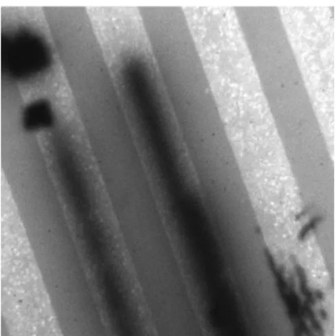
(4) Figure 1. (a) Compositions and thicknesses of the different layers that form the AlGaAs/GaAs laser diode; (b) schematic representation of the device (not to scale), illustrating the reference system used throughout this work. The shade/colour code establishes the correspondence between the individual layers in (a) and the structural components in (b). The CL measurements were done with a Gatan mono-CL2 system attached to a field emission scanning electron microscope (FESEM) (LEO 1530). The CL detection was done in single channel mode for the acquisition of the panchromatic CL images, with either a photomultiplier (PM) up to 900 nm, or an InGaAs photodiode for wavelengths longer than 800 nm reaching an upper wavelength limit of 1800 nm. For the spectrum analysis, a Peltier cooled Si CCD camera (200-1100 nm spectral range) was used. The typical acceleration voltages of our measurements range from 5 to 25 kV. The measurements were carried out at 80 K in order to improve the signal to noise ratio. 3. EXPERIMENTAL CHARACTERIZATION OF DEGRADED DEVICES Once the device has been catastrophically degraded, the panchromatic CL images reveal regions with dark contrast inside the cavity corresponding to the defects generated during the laser degradation process. As a rule of thumb, the areas with dark contrast adopt the form of dark lines, the so-called dark line defects (DLDs) [14], which are clusters of dislocations. Due to the multimode distribution in broad emitter lasers, the DLDs are spread out of the cavity axis (<110>). The DLDs are not related to a specific crystallographic orientation. They are led by the optical field which feeds energetically an absorbing region of the active zone of the laser, so that the change of orientation can be related to circulating modes [15]. However, as revealed in Figure 2, in lasers with injection channels, the DLDs follow the optical field, which is guided along those channels. The morphology and characteristics of the DLDs support certain hypotheses, which can be used to build up a model for the degradation process. High temperatures are reached in the active zone of the.
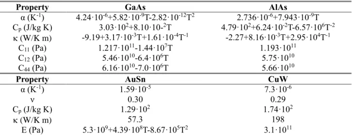
(5) laser, as observed by the presence of molten zones inside the DLD. Therefore, the COD can be considered as the result of a cocktail of thermal and mechanical effects ripened by some materials ingredients and the optical field absorption.. Figure 2. CL image of AlGaAs/GaAs laser showing the DLDs guided along the injection channels. The CL images of the degraded devices reveal regions with low, or fully quenched, radiative recombination activity, which are associated with the presence of extended defects in the active layers of the structure. This can occur at the facets and/or the inner cavity [15]. The normal operation of the laser over many hours prior to COD rules out the initial presence of grown-in, or processing induced dislocations in the active part. Dislocations are necessarily generated during the laser operation. The way the dislocations are generated and their fast progression to COD are differential aspects of this kind of degradation. 4. THERMOMECHANICAL MODEL The physical properties of the different materials that form the laser structure are listed in Table I [16– 24]. For those properties of the ternary alloys with significant contributions arising from lattice disorder, corrections are introduced via the Vegard’s law, with the corresponding bowing parameter [17]. A uniform local heat source, generated by the accumulation of energy in the defect rich region of the active zone, has been assumed [12,13]. The heat transfer equation has been solved using finite element methods (FEM). The limitations to the thermal conductivity, imposed by the low dimensionality and the phonon mismatch between layers [25–27], were explicitly considered. The quality of the interfaces and the presence of defects [28–30] can further reduce the thermal conductivity across the multilayer structures. The state of the art of the epitaxial growth of III-V compounds allows to fabricate layers of excellent crystalline quality. Therefore, the thermal resistance under normal operation is not contributed by defects. However, when the laser starts to degrade and dislocations are generated, the thermal conductivity will drop. Different effective/bulk conductivity (eff/bulk) ratios have been considered to track their role on the temperature distribution around the heat source. The initial.
(6) effective/bulk thermal conductivity ratio is estimated to be in the 0.34-0.25 range for the QW [25,31– 33], although it might be lower [27]. Property α (K-1) Cp (J/kg K) (W/K m) C11 (Pa) C12 (Pa) C44 (Pa) Property α (K-1) ν Cp (J/kg K) (W/K m) E (Pa). GaAs 4.24·10 +5.82·10-9T-2.82·10-12T2 3.03·102+8.10·10-2T -9.19+3.17·10-3T+1.61·10-4T-1 1.217·1011-1.44·107T 5.46·1010-6.4·106T 6.16·1010-7.0·106T AuSn 1.59·10-5 0.30 1.29·102 57.3 9 5.3·10 +4.39·108T-8.67·105T2 -6. AlAs 2.736·10 +7.943·10-9T 4.79·102+6.24·10-2T-6.57·106T-2 -2.27+8.16·10-3T+2.95·104T-1 1.193·1011 5.75·1010 5.66·1010 CuW 7.3·10-6 0.29 1.74·102 198 3.1·1011 -6. TABLE I. Main parameters of the materials used for the computations: α, thermal expansion coefficient; Cp, heat capacity; , thermal conductivity; C11, C12 and C44, elastic constants; ν, Poisson ratio; and E, Young’s modulus. The anisotropy of the thermal conductivity in nanoscaled layers has also been considered. Experimentally measured in-plane to cross-plane thermal conductivity ratios fluctuate from 1.2-1.3 [25,34,35] to 1.35-1.65 [31,33], whereas theoretical models predicted this ratio could be as high as 4 for GaAs QW structures [36]. Once the temperature distribution has been established, the solution provides the input for the thermomechanical equation. The system has been modelled in a classical continuum mechanical framework. Compared to our previous work[13], the model has been refined in a two-fold way. First, by explicitly considering the temperature dependence of the coefficient of thermal expansion (). The linear coefficient can be written as: 𝛼=. 1 𝑑𝑙 𝑙 𝑑𝑇. (1). where l is a particular dimension of the material. For small temperature variations dl/dT ≈ Δl/ΔT, so that the normal thermal strain components εi,th (i=x,y,z) can be approximately written as: 𝜀𝑖,𝑡ℎ = 𝛥𝑙/𝑙 = 𝛼 (𝑇 − 𝑇0 ). (2). where T0 is the stress-free reference temperature (roughly the operation temperature of the active layer of the laser), and T the temperature at each point of the geometry. However, for large temperature variations, Equation (1) has to be more rigorously integrated as:.
(7) 𝑇. ∫ 𝑇0. 𝑇 𝑇 𝑇 𝑑𝑙 𝑙(𝑇) 𝑙(𝑇) − 𝑙0 ∫ 𝛼(𝑇)𝑑𝑇 = 𝑙𝑛 ( ) = ∫ 𝛼(𝑇) 𝑑𝑇 ⇒ 𝜀𝑖,𝑡ℎ = = 𝑒 𝑇0 − 1 ≅ ∫ 𝛼(𝑇)𝑑𝑇 𝑙 𝑙0 𝑙0 𝑇0 𝑇0. (3). Given that (T) < 8·10-6 K-1 for all the AlxGa1-xAs compositions within the temperature range of interest (up to the melting point), the accuracy of the approximate expression is within 0.5% of the exact value. Second, the anisotropic elastic behaviour of the zinc blende (Al)GaAs materials has been taken into account. Whereas isotropic materials can be described just in terms of Young’s modulus and Poisson ratio, the elasticity matrix of a zinc blende system has three independent material elastic constants (C11, C12 and C44). 5. COMPUTATIONAL METHOD All the calculations have been performed using FEM within the framework of the commercially available program COMSOL Multiphysics®. In order to limit the computational requirements of the 3D problem, the LDs have been modelled for a cavity length of 50 m, significantly shorter than their nominal length (1200 m). The change in this factor, due to the very local effect of the heat source, has no relevant influence on the temperature and stress distributions. Thermal boundary conditions assume convective and radiative cooling on the device walls, and a fixed temperature (300 K) at the heat sink. For the mechanical counterpart, free displacement conditions have been defined for all the surfaces except for the bottom of the GaAs substrate, for which translation and rotation movements were excluded. The geometry was meshed into over 315 000 elements that correspond to over 1 000 000 degrees of freedom for the thermal problem and more than 3 000 000 for the mechanical part. The mesh was very dense for the QW and adjacent layers (close to 220 000 elements for just these 3 layers) with edge elements 2.4 nm apart around the heat source, and increasingly coarser as the distance from the QW grew. 6. RESULTS 6.1. Facet degradation Different numbers for the dimensions of the heat source/degraded region, for the heating power density, and for the reduced conductivity of the laser QW/barrier layer have been considered in order to determine the way in which these factors affect the temperature reached in the device, and how can they contribute to the degradation process..
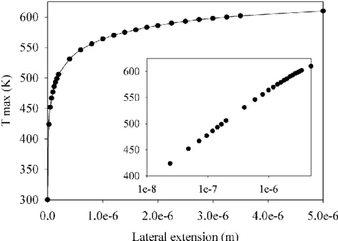
(8) When studying the facet heating, the vertical dimension (z axis, growth direction) of the heat source was chosen to encompass the thickness of the QW (12 nm), whereas the lateral extension (y axis) ranged from 24 nm to 5 m. For all the power densities and effective thermal conductivity ratios studied, a consistent trend in the relationship between the peak temperature in the QW and the size of the heat source was found. As it can be observed in Figure 3, the maximum temperature rapidly rises for lateral extensions in the range of the QW thickness. This growth is less prominent for dimensions exceeding 0.5-1 m. As illustrated in the inset, this dependence close resembles a logarithmic relation. The lateral extension of the heat source was set at 1 m for subsequent simulations.. Figure 3. Maximum temperature in the QW for eff/bulk = 0.25 and an 8 MW/cm2 power density as a function of the lateral extension of the heat source. The effect of the extension of the degradation inside the QW (x axis) was also inspected. This was done by assigning a reduced effective thermal conductivity to the degraded region. The maximum temperature in the QW is plotted as a function of the size of that portion in Figure 4. The temperature rises sharply up to about 12 nm and very slightly for higher values. Experimental evidence indicates that the depth of the degradation in samples that have gone through COD considerably exceeds the thickness of the QW [6]. Thus, when studying degrading devices the reduced conductivity ratios have been adopted for the whole of the QW layer..
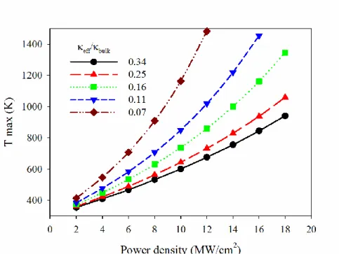
(9) Figure 4. Maximum temperature in the laser device as a function of the depth of the degraded region inside the laser cavity. eff/bulk was set at 0.16 for the degraded portion of the QW and at 0.34 for the rest of the layer. The power density for the heat source was 10 MW/cm2.. Figure 5. Maximum temperature in the laser diode as a function of the dissipated power density in the QW for a range of eff/bulk ratios. Please note that for eff/bulk values of 0.11 and 0.07, higher power densities than those represented would result in the QW melting..
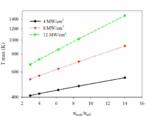
(10) Let us now consider the influence of the laser power density and the effective thermal conductivity ratio. For a typical cw emission of this type of devices, the absorbed laser power densities may lie between 0 and 10-12 MW/cm2 [13]. Figure 5 represents the local QW temperature as a function of the laser power density for different eff/bulk ratios. The temperature of the hot spot in the QW initially increases linearly with the laser power density absorbed, and becomes slightly superlinear for the highest powers. This behaviour is accentuated for the lower values of the eff/bulk ratio. As previously indicated, the eff/bulk ratio must be relatively high at the beginning of the process. For low eff/bulk ratios, it would be very difficult to reach the melting temperature. However, one can draw a scenario where the generation of dislocations, and a simultaneous increase of optical absorption, would progressively suppress the thermal conductivity. This would lead to a steeper temperature rise and to the thermal micro-explosion [37] or micro-ignition [38] that characterizes the thermal runaway. We will come back to this point later on. The influence of the reduced eff/bulk ratio is more clearly illustrated in Figure 6. The results are presented in terms of the reciprocal of this parameter (bulk/eff), i.e. the thermal resistivity ratio, for different power densities. The maximum temperature grows exponentially with the effective thermal resistivity. The exponential factor rises from (2.60±0.03)·10-2 for a power density of 4 MW/cm2, to (4.79±0.05)·10-2 for 8 MW/cm2, and to (7.05±0.04)·10-2 for 12 MW/cm2. This sharp increase in the slope should account for the thermal runaway.. Figure 6. Influence of the reciprocal of the conductivity ratio on the maximum temperature in the device for a range of absorbed power densities. Note the logarithmic scale for the y axis. Hence, of all the factors so far discussed, the reduced conductivity has the most drastic effect on the temperature reached at the QW hot spot. This is a very relevant observation. Virtually all the models.
(11) so far proposed to describe the operation of LDs have neglected the size effects on the thermal conductivity of the device, and the few that explicitly considered them [11,26] did not take into account the additional suppression that would be induced by the mechanical degradation. The in-plane to cross-plane anisotropy in the thermal conduction of the layers also affects the local temperature reached in the QW. Temperature profiles at the facet, both along the crystal growth and the transverse directions, are plotted in Figure 7. A surface plot has also been included to better illustrate how temperature is distributed. The inclusion of the anisotropy does not have any noteworthy influence in the shape of the curves for either the vertical (z) or the horizontal (y) directions. However, the anisotropy affects the absolute temperature values, which decrease as that factor grows. The traces for the anisotropic case with eff, in-plane/bulk=1.5·0.16=0.24 (triangle up) and to the isotropiceff /bulk=0.25 case (triangle down) are very close. The peak temperature is then largely determined by the in-plane conductivity (0.24≈0.25). The same trend is observed for the anisotropic eff, inplane/bulk=2·0.16=0.32 (crosshatch) and isotropic eff /bulk=0.34 (empty circle) cases.. Figure 7. Temperature profiles along the growth (a) and lateral (b) directions on the laser facet under a heat source with a power density of 6 MW/cm2 for various thermal conductivity ratios and anisotropy factors. The first figure in the legend for each plot accounts for the eff/bulk ratios, while the second number relates to the in-plane/cross-plane anisotropy. (c) Surface temperature plot for the central layers at the facet of the device for isotropic eff/bulk = 0.16 and 6 MW/cm2..
(12) The temperature, as shown in Figure 7.c, drastically decreases outside the volume occupied by the heat source: the highest temperature in the cladding layer closest to the guides is 345 K, whereas the peak temperature in the laser is about 527 K. These large gradients may raise concerns about the meaning or the very applicability of “temperature” for this range of dimensions. This question has been put forward before [39,40]: though the classical definition is entirely local, the quantum counterpart requires the region in which it is defined to be larger than the mean-free-path of the phonons. Regardless of this disquisition, temperature is still used for the description of nanoscaled systems, and nanoscopic resolution in the measurement of temperatures is claimed for experimental techniques such as scanning thermal microscopy and nano-thermal analysis [40]. The anisotropy factor has been handled with care in the calculations. As recently reported [25], disorder (atomistic mixing) in the layers would lower the anisotropy ratios. Therefore, in our model of progressively deteriorating thermal conductivities, we have considered this factor just for the initial operational condition of the device. The accumulation of dislocations in later stages would essentially cancel out the anisotropy. In what follows, for a state-of-the art device [25], an initial eff, cross-plane/bulk value of 0.25 is assumed, while the anisotropy is set at 1.35. These figures virtually lead to the same results as an isotropic thermal conductivity with a 0.34 effective/bulk ratio. Therefore, the effective thermal conductivity under degradation will be described in terms of a decreasing eff/bulk ratio, keeping in mind that the 0.34 data really correspond to the initial anisotropic behaviour.. Figure 8. Tresca stress profiles along the growth (z) direction on the laser facet under a power density of 6 MW/cm2 heat source as a function of the thermal conductivity ratio. When the mechanical counterpart of the system is solved, a distinctive trend is observed. Among the various theories devised for the evaluation of the onset of plastic deformation, we have adopted the Tresca criterion (shear stress), although the results would be very similar if other, e.g., the von Misses.
(13) theory, had been chosen. The calculated Tresca stress profiles are represented in Figure 8 across the central layers of the laser structure as a function of the thermal conductivity ratio. Large gradients closely following the temperature pattern are observed. The steep changes in temperature lead to drastic variations of the mechanical stresses, which are further accentuated by the discontinuity of the mechanical properties at the barrier layers-QW interfaces (z = ± 6 nm). If the calculated maximum stresses are plotted in terms of the QW peak temperatures (see Figure 9), all the computed data are accumulated along a line, regardless of the specific figures (power density, eff/bulk ratios, dimension of the heat source) used for the calculations. That characteristic line defines the thermomechanical behaviour of the laser when a local heat source is present. The data plotted in Figure 9 permit to analyse the experimental conditions that will drive to the laser degradation.. Figure 9. Maximum shear stress versus peak QW temperature for different heat source dimensions, thermal conductivity ratios and absorbed power densities. The circles and the squares correspond to a eff/bulk ratio of 0.25: in the first case, the power density is fixed at 10 MW/cm2 and the lateral extension of the heating source ranges from 0.025 to 2.5 m; in the latter, the lateral dimension is set at 1 m, whereas the power density varies between 2 and 18 MW/cm2, with a 2 MW/cm2 step size. The triangles and the diamonds are the data for eff/bulk ratios of 0.34 and 0.16 respectively, the other conditions as for the squares. 6.2. In cavity degradation The model has been extended to analyse the outcome of a similar (2D) heat source inside the laser cavity. Roughly speaking, in order to give rise to a temperature profile similar to that for the facet, twice the power has to be absorbed by the source inside the QW. This is illustrated in Figure 10, where.
(14) the results for different eff/bulk ratios are plotted for a power density of 12 MW/cm2. If compared with Figure 7, which was obtained for a 6 MW/cm2 source at the facet with identical dimensions, only slight differences can be appreciated.. Figure 10. Temperature profile along the growth direction at the plane of an inner 12 MW/cm2 heat source for different thermal conductivity ratios. The source is located at 0.5 m from the facet. This is due to the differences in the thermal boundary conditions. In our model, heat exchange between the facet and the surrounding air, through both radiative and convective mechanisms, is allowed. Nevertheless, when the global outgoing heat flux through this surface is evaluated, it amounts to less than 7·10-3 % of the total absorbed power. Therefore, this boundary condition for facet heating is virtually identical to thermal insulation or, equivalently, to a symmetry condition. Thus, the solution for the source on the facet is also valid for a heat source twice as intense placed inside the QW channel. The results correlate well with these considerations provided that neither the front nor the rear mirrors are too close to the actual position of the heat source. The temperature distribution along the cavity is shown in Figure 11 for the same conditions as in Figure 10. As the distance of the source from the facet is shortened, the asymmetry in the temperature decay on the opposite sides of the heat source is accentuated, and the peak temperature rises progressively approaching, as expected, the values obtained for facet heating. When the mechanical counterpart is solved, further differences arise. In the case of the mirror heating, free displacement conditions were set for the facet. In the present case, the continuity of the layer is set up for the heat source plane. This results in noticeably lower stresses for equivalent temperatures. As shown in Figure 12, peak values of stress and temperature inside the cavity are correlated, showing a similar alignment to that obtained for the facet. However, not only the absolute stress values are lower inside the cavity, but a significantly smaller slope is also obtained from the curve..
(15) Figure 11. Temperature profile inside a QW with thermal conductivity ratio eff/bulk =0.34 for a 12 MW/cm2 heat source placed at a distance of 0.5 m from the facet.. Figure 12. Tresca stress versus peak QW temperature for an inner heat source in terms of eff/bulk ratios and absorbed power densities. The power densities vary between 2 and 10 MW/cm2, with a 2 MW/cm2 step size. The dashed line illustrates the behaviour in the case of facet heating, Figure 9..
(16) 7. DISCUSSION According to the previous analysis, one can set up a scenario for the COD. A series of successive steps leading to the degradation can be distinguished: 1) the process will start with a local temperature rise leading to a bandgap shrinkage in the QW; 2) the thermal stresses, produced by the local heat source feedback by the laser absorption, generate dislocations; 3) dislocations multiply under the action of the thermal stresses and light absorption, and 4) the thermal conductivity is progressively suppressed by the presence of defects leading to a local accumulation of energy ending by the thermal runaway process. The initial stages of the degradation of LDs have been rationalized [8,41–43] in terms of non-radiative recombination, either surface recombination at the facet or at point defects inside the QW. The last decades view a persistent improvement of the laser structures. Therefore, the density of defects has been drastically reduced to significantly enhance the laser reliability. However, the concentration of these defects steadily grows as a result of the laser operation, and this increase would be responsible for the initially very slow drop in optical power of the device. The need for new experimental techniques to adequately monitor this progressive degradation has been brought forth [42]. Non-radiative recombination processes can transfer the released energy as heat to the crystal lattice. The concomitant heating leads to bandgap shrinkage and a variation of the laser parameters characterizing the wear out degradation. The catastrophic degradation is strongly related to the laser light self-absorption, which can only be achieved via the existence of hot spots inside the active zones. These can absorb the laser light generated in the regions of the cavity that remain “cold”. This initial heating must be associated with the accumulation of defects in small volumes of the active zone. Surface defects would play this role at the facet. On the other hand, the defects generated inside the cavity as a result of the aging process must be present in higher concentration in tiny regions of the active layers in which they tend to accumulate. The heating of these specific regions makes them laser absorption sites. Therefore, one can argue that the laser degradation is incubated in those regions during the wear out degradation [8]. It should also be born in mind that the non-radiative recombination, the enhanced temperature, and the corresponding thermal stresses can effectively lower the threshold barriers for defect formation and migration via recombination enhanced defect reactions (REDR) [44,45]. This feedback mechanism further raises the temperature during laser operation. An alternative/supplementary path for heat generation can be launched by a local resistivity reduction due to the accumulation of point defects, which could produce a current crowding [46] that would give rise to a local Joule heating effect. Chen and Tien [11] proposed an alternative route in which intrinsic laser light absorption in the guides played a key role in the degradation process. In the previous section we have shown that the temperature is very inhomogeneously distributed. The barrier and cladding layers can be considered “cold” with respect to the QW. Furthermore, they have a bandgap significantly larger than the QW. Unless the temperatures in these layers rise to about 750 K [22], these are virtually non-absorbing media. As we shall see below, we expect a noticeable mechanical degradation of the active layers before this temperature is reached, so that extrinsic defect-mediated light absorption in the guides is most likely to occur prior to the activation of the intrinsic absorption mechanisms..
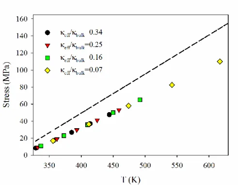
(17) Up to this point, the laser is in a wear out failure mode. The evolution of the laser will be governed by the local temperatures and the thermal stresses. In other words, it would depend on the operating conditions in the presence of the hot spot. The evolution of the laser is summarized in the plots of Figures 9 and 12 for facet and inner cavity degradation, respectively. In the frame of our thermomechanical model, the COD is triggered once a critical temperature, at which dislocations are generated due to the thermal stresses, is reached. In previous works [4,13] we expected the onset of the COD process to occur at the crosshatch of the calculated Tresca stress – peak temperature data and the experimental curve for the yield strength of GaAs. For a facet heat source, this concurrence establishes a critical temperature of about 480 K. In a recent publication [12] we discussed the difference between this estimated local temperature and the commonly reported critical temperatures for COD, as derived from techniques with a micrometric resolution. A distribution with a maximum of 480 K leads to a very low mean temperature compared to the experimental values [12]. Once more, the differences between bulk properties and their low dimensional scale counterparts must be invoked. We have already argued about their capital influence on the thermal conductivity, but now is the time to focus on the mechanical behaviour [47–49]. Whereas the stress-strain relationships on the microscale have been found to be very similar to those of the bulk, remarkably high sub-micron yield strengths have been reported for different materials [47,50–52]. This has been rationalized in terms of different mechanisms, such as the Hall-Petch [50,53,54] or modified confined layer slip (CLS) models [51,55]. These schemes, suggested for different materials, describe the yield strength as defined by the characteristic lowest dimension of the system (h). The two models hold different dependence relations: h-1/2 for Hall-Petch, and ln(h)/h for the modified CLS models, respectively. Unfortunately, a limited amount of information exists for the mechanical behaviour of GaAs in the micro- and nanoscales [56–58]. Whereas no strengthening effect is apparently observed for micropillars with a 10 m diameter [58], the yield strength increases by a factor of approximately 1.35 when that diameter is reduced to 1 m [56]. A more drastic departure from bulk values was observed for GaAs nanowires, for which an enhancement of Young’s modulus was reported [57]. According to these works, the behaviour of GaAs would follow similar trends to those of metal-based systems, and would account for a significant endurance of QWs. It is hard to assess the change in the yield strength for our particular QW system from the presently available experimental results. Nevertheless, we will make some rough approximations assuming that the Hall-Petch model governs the mechanical properties of the thinnest layers in the laser diode. Extrapolating the quoted data [56,58], we estimate the yield strength for the 130 nm thick guide layers to be approximately 2.8 times the bulk value, while for the 12 nm thick QW it would rise to about 9 times the bulk figures. This difference between the expected mechanical strength at the QW and the adjacent layers raises the question of where the thermal stresses would overcome the yield stress first: inside the QW or at the QW-guide interface. Figure 13 illustrates this point. The lines correspond to the experimental bulk yield stress data [59,60] and to the estimations for the 12nm (QW thickness) and 130 nm (waveguide thickness) layers. The points stand for the computed Tresca stress versus maximum temperature pairs both in the QW and in the guiding layers. We assume that, up to this point, the thermal conductivity remains almost unaltered so that bulk/eff is set at 0.34..
(18) Figure 13. Experimental yield strength for bulk GaAs (solid line), and estimated behaviour for 130 nm (dotted line) and 12 nm (dashed line) thick films, considering the Hall-Petch effect. The symbols correspond to the data for bulk/eff=0.34 and for power densities from 2 to 14 MW/cm2 with a 2 MW/cm2 step size, evaluated either in the QW (circles) or at the QW-guide interfaces (triangles). The first conclusion derived from this figure is that in previous works we had underestimated the temperature that initiates the COD. The crossing of the computed data and the yield stress (corrected for the reduced dimensions) lead to critical temperatures significantly higher than our previous estimation: approximately 520 K for the guide and 630 K for the QW. In order to reach the 520 K mark in the guide, a heating power density slightly over 10 MW/cm2 would be required. A power density in excess of 11 MW/cm2 would be needed for 630 K to be generated in the QW. It should be stressed that 520 K corresponds to the temperature in the guide, not to the maximum temperature in the device (about 600 K for 10 MW/cm2). According to these reassessments, the mechanical degradation could be expected to start either inside the QW or at QW-guide interface, though it would be slightly more likely to be initiated at the interface. The mechanical strengthening of the QW and the guiding layers requires higher thermal stresses for dislocations to be generated than we had previously estimated. As a direct consequence, a better agreement of our model with the (experimentally averaged) critical temperatures is reached. The corrections applied to the mechanical behaviour should be refined as more detailed experimental data become available. Our assumption that the strengthening effect starts for dimensions just under 10 m may be inaccurate, and a transition from bulk to low-dimensionality behaviour for smaller values is more likely to be expected. This would lead to more pronounced changes in the size dependent yield stress, so that 600K should be considered as a lower limit for the peak temperature in the QW to bring about COD..
(19) Furthermore, it should also be considered whether the small dimensions and the prominent stress gradients which are generated might rule out the application of standard linear mechanical analysis. A study on GaAs quantum dots estimated relevant size dependent mechanical effects for those structures [61], whereas a more recent work from the same research group apparently ruled out the need for this refined approach except at an unreasonably small scale [62]. This issue will be addressed in forthcoming works. Once the yield stress is reached, the following stage in the degradation of the device would basically be the same, regardless of whether the dislocations are initially formed inside the QW or the guide. The number of extended defects would rapidly multiply and, for the temperatures and stresses considered in the active region of the device, they would readily propagate across the central layers [45]. This gives rise to a two-fold effect. On the one hand, as previously discussed, it results in rapidly decreasing thermal conductivities. On the other hand, it activates extrinsic mechanisms for laser light absorption that increase notably the dissipated power. Both effects bring about higher temperatures in a feedback mechanism that would lead to thermal runaway.. Figure 14. Proposed thermal path to COD. The path to COD according to our model is summarized in Figure 14. The peak temperature is plotted in terms of the laser power density and the effective thermal conductivity ratio. The dashed line superposed to the plot represents the thermal runaway path. Initially the local temperature is increased while the thermal conductivity retains its original value. The boosted optical absorption produces a further growth of the temperature following a nearly linear relationship. When the critical temperature is reached, dislocations are generated, and extrinsic light absorption and a drastic drop in the thermal conductivity are brought forth. These effects cause a pronounced superlinear temperature rise (see the projection of the path on the back plane of the figure) leading to a sudden melting, characteristic of.
(20) the thermal runaway. In the case of an inner heat source, the lower slope of the Tresca stress versus temperature plot leads to higher critical temperatures. With the same assumptions as above, the crossing point would be approximately 30 K higher than the one reported for the facet. The COD is less likely to occur in the cavity, not only because a better dissipation of the heat is achieved inside the QW, but also because the build-up of the mechanical stresses is milder than at the facet. These effects are inherent to the diverse thermal and mechanical (boundary) conditions at the heat source on the two situations, and clearly explain why mirror damage is more common than bulk damage in this type of laser. In order to reach a peak temperature of around 630 K inside the QW, if the thermal conductivity is again assumed to remain almost unaltered up to that point, the power density should be in excess of 22 MW/cm2, which is an unreasonably large number for the LD [13]. This density might be locally reached, however, if self-focusing of the laser light is induced by thermal lensing effects [42]. Alternatively, the question whether the initial thermal conductivity ratio here chosen is too conservative should be brought forth. According to the estimations in the previous works that explicitly considered these size effects [11,26], that may indeed be the case. If, in consonance with those models, an effective value for the thermal conductivity about an order of magnitude smaller than that of the bulk is used from the beginning of the process, a more reasonable power density of about 12 MW/cm2 would be sufficient to give rise to in-cavity COD. Of course, if this option is also applied to the description of COD at the facet, notably lower power density conditions need be met: in this case, about 6 MW/cm2 yield to a peak temperature over 600 K in the QW. Whether talking about COD at the facet or inside the cavity, the thicknesses of the guides and the QW play very relevant roles. Reducing the size has a favourable outcome in terms of the mechanical stability of the structures, whereas it leads to poorer thermal conductivities, so that a compromise between these conflicting behaviours should be reached. These considerations can be set as the basis for a controlled design of the LDs in order to produce more robust devices. Fundamental factors that determine the operation of QW LDs [63], such as the increased differential gain in the QW, the beam size limitation via the separate confinement structure or the threshold current density of the device, all of which also depend on the dimensions of these central layers, must obviously dictate the design of the lasers. But these thermal and mechanical effects should be brought forth, especially for applications that require extended durability, such as undersea optical communications.. 8. CONCLUSION A thermomechanical model has been proposed to describe the degradation of an AlGaAs/GaAs GRINSCH laser diode. The departure of the materials properties in the nanoscopic layers from those of the bulk, both for the thermal and the mechanical characteristics, has been explicitly considered. The model has been solved in a 3D scheme using FEM, both for facet and for in-cavity power dissipation mechanisms. Very inhomogeneous distributions of temperatures and stresses are derived from the computations, and typical trends in the building up of the thermal stresses have been identified. The onset of the mechanical degradation, which leads to the formation of extended defects.
(21) and dislocations, as well as to the triggering of the COD, has been estimated considering the mechanical strengthening size effects for the QW and the guiding layers. A feasible path to COD has been proposed. It should be stressed that the thermomechanical conditions that trigger the COD depend on the properties of the active layers, so that a modification of the composition of the QW or the guide layers would result in another set of conditions and, under certain circumstances, diverging stages in the degradation mechanism. For example, if the concentration of Al in the guide layers is closer to that in the QW for a specific laser diode configuration, intrinsic absorption of the laser light in the guide may be triggered before the yield strength is reached, and should therefore be considered as a relevant factor in the degradation process. This subject opens the path for a systematic approach for improving the device reliability and will be further pursued in forthcoming work. ACKNOWLEDGMENTS This work was funded by the Spanish Government (ENE2014-56069-C4-4-R) and Junta de Castilla y León (VA293U13 and VA081U16 (003)). J. L. Pura was granted by the FPU programme of the Spanish Government (FPU14/00916).. References [1]. Tomm J W and Jiménez J 2006 Quantum Well Laser Array Packaging (New York: McGrawHill) [2] Jiménez J 2003 Laser diode reliability: Crystal defects and degradation modes Comptes Rendus Phys. 4 663–73 [3] Welch D F 2000 A Brief History of High-power Semiconductor Lasers IEEE J. Sel. Top. Quantum Electron. 6 1470–7 [4] Hortelano V, Anaya J, Souto J, Jiménez J, Perinet J and Laruelle F 2013 Defect signatures in degraded high power laser diodes Microelectron. Reliab. 53 1501–5 [5] Souto J, Pura J L, Torres A, Jimenéz J, Bettiati M and Laruelle F J 2016 Catastrophic optical damage of high power InGaAs/AlGaAs laser diodes Microelectron. Reliab. 64 627–30 [6] Souto J, Pura J L, Rodríguez M, Anaya J, Torres A and Jimenéz J 2015 Mechanisms driving the catastrophic optical damage in high-power laser diodes Proc. SPIE 934893480O [7] Fukuda M 1991 Reliability and Degradation of Semiconductors Lasers and LEDs (Boston: Artech House) [8] Ueda O 2010 On degradation studies of III-V compound semiconductor optical devices over three decades: Focusing on gradual degradation Jpn. J. Appl. Phys. 49 90001 [9] Henry C H, Petroff P M, Logan R a. and Merritt F R 1979 Catastrophic damage of AlxGa1xAs double-heterostructure laser material J. Appl. Phys. 50 3721–32 [10] Nakwaski W 1990 Thermal model of the catastrophic degradation of high-power stripegeometry GaAs/(AlGa)As double-heterostructure diode lasers J. Appl. Phys. 67 1659.
(22) [11] [12] [13] [14] [15] [16] [17] [18] [19] [20] [21] [22] [23] [24] [25]. [26] [27] [28] [29] [30]. Chen G and Tien C L 1993 Facet heating of quantum well lasers J. Appl. Phys. 74 2167–74 Souto J, Pura J L and Jiménez J 2016 About the physical meaning of the critical temperature for catastrophic optical damage in high power quantum well laser diodes Laser Phys. Lett. 13 25005 Martín-Martín A, Avella M, Iñiguez M P, Jiménez J, Oudart M and Nagle J 2009 Thermomechanical model for the plastic deformation in high power laser diodes during operation J. Appl. Phys. 106 73105 Waters R G 1991 Diode laser degradation mechanisms: A review Prog. Quantum Electron. 15 153–74 Hempel M, Tomm J W, Hortelano V, Michel N, Jiménez J, Krakowski M and Elsaesser T 2012 Time-resolved reconstruction of defect creation sequences in diode lasers Laser Photon. Rev. 6 L15–9 Adachi S 1983 Lattice thermal resistivity of III-V compound alloys J. Appl. Phys. 54 1844–8 Adachi S 1985 GaAs, AlAs, and AlxGa1−xAs: Material parameters for use in research and device applications J. Appl. Phys. 58 R1–29 Adachi S 2007 Lattice thermal conductivity of group-IV and III-V semiconductor alloys J. Appl. Phys. 102 63502 Krieger M, Sigg H, Herres N, Bachem K and Köhler K 1995 Elastic constants and Poisson ratio in the system AlAs-GaAs Appl. Phys. Lett. 682 682 Gehrsitz S, Sigg H, Herres N, Bachem K, Köhler K and Reinhart F 1999 Compositional dependence of the elastic constants and the lattice parameter of AlxGa1-xAs Phys. Rev. B 60 11601–10 Burenkov Y A, Burdukov Y M, Davidov S Y and Nikanorov S P 1973 Temperature dependences of the elastic constants of gallium arsenide Sov. Phys. Solid State 15 1175–7 Madelung O, Osten W von der and Rössler U 1987 Intrinsic Properties of Group IV Elements and III-V, II-VI and I-VII Compounds ed O Madelung (Berlin: Springer-Verlag) Glazov V M and Pashinkin A S 2000 Thermal expansion and heat capacity of GaAs and InAs Inorg. Mater. 36 225–31 Martienssen W and Warlimont H 2005 Springer Handbook of Condensed Matter and Materials Data (Berlin: Springer-Verlag) Luckyanova M N, Johnson J A, Maznev A A, Garg J, Jandl A, Bulsara M T, Fitzgerald E A, Nelson K A and Chen G 2013 Anisotropy of the thermal conductivity in GaAs / AlAs superlattices Anisotropy of the thermal conductivity in GaAs / AlAs superlat- tices Nano Lett. 13 3973–7 Tan H, Kamath K K, Mi Z, Bhattacharya P and Klotzkin D 2006 Analysis of the reduced thermal conductivity in InGaAs/GaAs quantum dot lasers from chirp characteristics Appl. Phys. Lett. 89 1–3 Balandin A and Wang K 1998 Significant decrease of the lattice thermal conductivity due to phonon confinement in a free-standing semiconductor quantum well Phys. Rev. B 58 1544–9 Hopkins P E 2013 Thermal transport across solid interfaces with nanoscale imperfections: Effects of roughness, disorder, dislocations, and bonding on thermal boundary conductance ISRN Mech. Eng. 2013 682586 Luo T and Chen G 2013 Nanoscale heat transfer--from computation to experiment. Phys. Chem. Chem. Phys. 15 3389–412 Liang L H and Li B 2006 Size-dependent thermal conductivity of nanoscale semiconducting.
(23) [31] [32] [33] [34] [35] [36] [37] [38] [39] [40] [41] [42] [43] [44] [45] [46] [47] [48] [49] [50] [51]. systems Phys. Rev. B - Condens. Matter Mater. Phys. 73 1–4 Yao T 1987 Thermal properties of AlAs/GaAs superlattices Appl. Phys. Lett. 51 1798–800 Yu X Y, Chen G, Verma A and Smith J S 1995 Temperature dependence of thermophysical properties of GaAs/AlAs periodic structure Appl. Phys. Lett. 67 3554–6 Capinski W, Maris H, Ruf T, Cardona M, Ploog K and Katzer D 1999 Thermal-conductivity measurements of GaAs/AlAs superlattices using a picosecond optical pump-and-probe technique Phys. Rev. B 59 8105–13 Yang B, Liu W L, Liu J L, Wang K L and Chen G 2002 Measurements of anisotropic thermoelectric properties in superlattices Appl. Phys. Lett. 81 3588–90 Yang B and Chen G 2003 Partially coherent phonon heat conduction in superlattices Phys. Rev. B 67 1–4 Chen G and Tien C L 1993 Thermal conductivities of quantum well structures J. Thermophys. Heat Transf. 7 311–8 Eliseev P G 1973 Degradation of injection lasers J. luminiscence 7 338–56 Tomm J W, Ziegler M, Hempel M and Elsaesser T 2011 Mechanisms and fast kinetics of the catastrophic optical damage (COD) in GaAs-based diode lasers Laser Photon. Rev. 5 422–41 Cahill D G, Ford W K, Goodson K E, Mahan G D, Majumdar A, Maris H J, Merlin R and Phillpot S R 2003 Nanoscale thermal transport J. Appl. Phys. 93 793–818 Cahill D G, Braun P V., Chen G, Clarke D R, Fan S, Goodson K E, Keblinski P, King W P, Mahan G D, Majumdar A, Maris H J, Phillpot S R, Pop E and Shi L 2014 Nanoscale thermal transport. II. 2003-2012 Appl. Phys. Rev. 1 Jimenez J, Anaya J, Hortelano V, Souto J and Martin-Martin A 2013 Degradation signatures of high power laser diodes Proceedings of the 2013 Spanish Conference on Electron Devices, CDE 2013 Sin Y, Presser N, Brodie M, Lingley Z, Foran B and Moss S C 2015 Degradation mechanisms in high-power multi-mode InGaAs-AlGaAs strained quantum well lasers for high-reliability applications 934893480L Eliseev P G 1996 Optical strength of semiconductor laser materials Prog. Quantum Electron. 20 1–82 Maeda K, Sato M, Kubo A and Takeuchi S 1983 Quantitative measurements of recombination enhanced dislocation glide in gallium arsenide J. Appl. Phys. 54 161–8 Sugiura L 1997 Comparison of degradation caused by dislocation motion in compound semiconductor light-emitting devices Appl. Phys. Lett. 70 1317 Eliseev P G, Glebov A G and Osiński M 1997 Current self-distribution effect in diode lasers: Analytic criterion and numerical study IEEE J. Sel. Top. Quantum Electron. 3 499–506 Gerberich W W, Michler J, Mook W M, Ghisleni R, Östlund F, Stauffer D D and Ballarini R 2009 Scale effects for strength, ductility, and toughness in “brittle” materials J. Mater. Res. 24 898–906 Zhu T and Li J 2010 Ultra-strength materials Prog. Mater. Sci. 55 710–57 Maharaj D and Bhushan B 2015 Friction , wear and mechanical behavior of nano-objects on the nanoscale Mater. Sci. Eng. R 95 1–43 Maharaj D and Bhushan B 2014 Scale effects of nanomechanical properties and deformation behavior of Au nanoparticle and thin film using depth sensing nanoindentation Beilstein J. Nanotechnol. 5 822–36 Misra A, Hirth J P and Hoagland R G 2005 Length-scale-dependent deformation mechanisms.
(24) [52] [53] [54] [55] [56] [57] [58] [59] [60] [61] [62] [63]. in incoherent metallic multilayered composites Acta Mater. 53 4817–24 Uchic M D, Dimiduk D M, Florando J N and Nix W D 2004 Sample dimensions influence strength and crystal plasticity Science (80-. ). 305 986–9 Hall E O 1951 The deformation and ageing of mild steel III Discussion of results\t Proc. Phys. Soc. Sect. B 64 747–53 Petch N J 1953 The cleavage strength of polycrystals J. Iron Steel Inst. 174 25–8 Ghoniem N M and Han X 2005 Dislocation motion in anisotropic multilayer materials Philos. Mag. 85 2809–30 Michler J, Wasmer K, Meier S, Östlund F and Leifer K 2007 Plastic deformation of gallium arsenide micropillars under uniaxial compression at room temperature Appl. Phys. Lett. 90 88–91 Wang Y B, Wang L F, Joyce H J, Gao Q, Liao X Z, Mai Y W, Tan H H, Zou J, Ringer S P, Gao H J and Jagadish C 2011 Super deformability and young’s modulus of gaas nanowires Adv. Mater. 23 1356–60 Ghisleni R, Liu J, Raghavan R, Brodard P, Lugstein A, Wasmer K and Michler J 2011 In situ micro-Raman characterization of plasticity and fracture in GaAs Philos. Mag. 91 1286–92 Suzuki, T. Yasutomi, T. T. Okuoka, T 1999 Plastic deformation of GaAs at low temperatures Philos. Mag. A 79 2637–54 Wang S and Pirouz P 2007 Mechanical properties of undoped GaAs. Part I: Yield stress measurements Acta Mater. 55 5500–14 Zhang X and Sharma P 2005 Size dependency of strain in arbitrary shaped anisotropic embedded quantum dots due to nonlocal dispersive effects Phys. Rev. B - Condens. Matter Mater. Phys. 72 195345 Maranganti R and Sharma P 2007 A novel atomistic approach to determine strain-gradient elasticity constants: Tabulation and comparison for various metals, semiconductors, silica, polymers and the (Ir) relevance for nanotechnologies J. Mech. Phys. Solids 55 1823–52 Svelto O 2010 Principles of Lasers (Boston, MA: Springer US).
(25)
Figure
+7


Documento similar
The scope of this Thesis is the investigation of the optical properties of two systems based on semiconductor nanostructures: InAs/GaAs quantum rings embedded in photonic
In the previous sections we have shown how astronomical alignments and solar hierophanies – with a common interest in the solstices − were substantiated in the
Li, Investigation on the flow and convective heat transfer characteristics of nanofluids in the plate heat exchanger, Experimental Thermal and Fluid Science 76
influence of these parameters on the size and distribution of Te inclusions, deep defects, optical and electrical properties of CdZnTe detectors. In the fourth chapter, the effect
Two cases are considered, the one for which the symplectic form on the torus is of integer cohomology class n (section 4.1), where full modular invariance is obtained only when the
CFD simulations for different Reynolds numbers provide a further insight into the relation of the flow structures with wall shear stress, and their role on the local heat
Next, in sections 7 and 8, the influence of the different elements/characteristics of the standard (termination, airline, thermal bead, level of liquid Nitrogen, etc.)
MD simulations in this and previous work has allowed us to propose a relation between the nature of the interactions at the interface and the observed properties of nanofluids:
