A multilevel modular dc dc converter topology
25
0
0
Texto completo
(2) Highlights Click here to view linked References. Highlights . A DC-DC Modular Multilevel Converter based on a double П configuration is presented. The topology uses cascaded H-Bridge converters. A two level control hierarchy regulates the DC link voltage of each H-bridge module. At top level, DC and AC signals are used for energy control in each branch. At low level, AC signals control the H-bridge DC voltages within each branch..
(3) Manuscript Click here to view linked References. A multilevel modular dc-dc converter topology a. Ricardo Vidal, bDiego Soto, cIván Andrade, dJavier Riedemann, cCristián Pesce, aEnrique Belenguer, c Rubén Peña, eRamón Blasco-Gimenez a Universitat Jaume I University of Magallanes c University of Concepción d University of Bío-Bío e Universitat Politècnica de València b. Corresponding Author Cristián Pesce, University of Concepción, Edmundo Larenas 219, Concepción, Chile. Phone +56-41-2204259, [email protected]. Abstract– A multilevel modular DC-DC power conversion topology based on cascaded H-Bridge converters in a double П configuration is presented. The topology is intended to interconnect large power DC networks. A two level control hierarchy is used to regulate the DC voltage of each H-bridge module. At the top level, DC and circulating AC currents are used to control the total energy converter in all branches (both parallels and series) of each П arrange. At bottom level, the voltage balance of a converter branch, which comprises N H-bridge modules, is carried out by balancing (N-1) capacitor voltage deviations, with respect to the average capacitor voltage. The entire topology and control strategies are simulated in a PSIM environment. Simulation results with three H-bridge converters per branch are shown and preliminary experimental results with a low power prototype are also included. Keywords – DC-DC converter, Multilevel Modular Converter, HVDC Applications. 1. Introduction The modular multilevel conversion approach introduced by Marquardt [9] and referred as to the Modular Multilevel Converter (MMC) topology has become the choice topology for high voltage, high power VSC (Voltage Source Converter) HVDC (High Voltage Direct Current) converter station [5], [16]. Like the standard two-level VSC, the MMC is typically arranged in a standard converter topology, such as a three-phase bridge, but it uses a string of half, or full, bridge converter modules instead of a string of IGBTs as high voltage valve [1]. This allows valves to operate in a multilevel.
(4) conversion fashion offering advantages such as high quality voltage and current waveforms; low switching frequency, hence low power loss; and because of the simple building block (e.g. half bridge module) a highly modular design approach to meet the high voltage and power levels required for HVDC applications.. Because of its successful application to HVDC systems, the MMC is being considered for applications other than AC-DC conversion. These include modular multilevel DC-DC conversion topologies such as those proposed in [4], [8], [11], [12], [13]. This technology may be suitable to interconnect HVDC systems by their DC sides so as to implement a HVDC grid [3], [7]. The topology in [8] and [12] is basically a cascade of two standard AC-DC MMC stages which are connected by its AC sides. The first MMC implements the DC-AC conversion stage, of moderate frequency, whereas the second MMC implements the AC-DC conversion stage. A similar alternative but based on the Alternating Arm Converter (AAC) is proposed in [11]. Several topologies, not exactly thought as DC-DC converters with an intermediate AC link are proposed in [3] and [4].. The modular multilevel DC-DC proposed here is based on the modular multilevel frequency changing converter introduced in [15]. This topology has three MMC branches arranged in a PI topology: A series branch, connected between the input and output, and two parallel branches. One of the parallel branches is connected at the input and it is referred as a shunt branch, and the other is connected at the output and it is referred as a derivation branch. The DC-DC converter consists of six branches arranged in a double П topology, as shown in Fig. 1. Each branch can have N H-Bridge converter modules. The top and bottom halves of the converter (П topologies) operate in a similar manner.. Compared to alternative MMC based DC-DC power converter topologies, such as those using intermediate AC links [9] and [12], the double П topology for DC-DC conversion proposed in this work does not require intermediate coupling transformers and may require smaller silicon area, i.e. summation of volt amp product of power semiconductor devices to implement the overall power converter..
(5) Fig.1: Multilevel Modular DC-DC proposed Converter. One of the main challenges in MMC topologies is to keep the DC voltage capacitor in each cell (either for full or half H-bridge) within certain range in order to operate the power devices safely and ensuring the control of the converter current. The energy balance between the total amount of energy stored in the capacitors in a branch and the energy supplied from those capacitors, within a time window, is a key factor to maintain capacitor voltages within the nominal values [2], [6], [14], [15]. In other words, the average power shared between each branch and the system has to be, neglecting losses, null. In [8], [11], [12] the energy balance is achieved by imposing a current in each branch which contains a component at the intermediate. AC frequency (set to 100Hz as discussed in section. 2.2) and a DC component. In this way the total energy stored in a branch can be fully regulated. The topologies in [4], like the one proposed here, do not use an intermediate AC link but they also require an AC voltage and current component to enable converter branches to exchange power, hence energy, with the system at a component other than the DC one. This auxiliary AC component, referred as to secondary frequency component in [4], will provide energy balance at the branch level in the double PI DC-DC topology. The energy balance within a particular branch, i.e. the DC voltage balance in each cell in the branch, can be carried out, for instance, as proposed in [15] or exploiting the commutation redundant states as described in [11] and [14]..
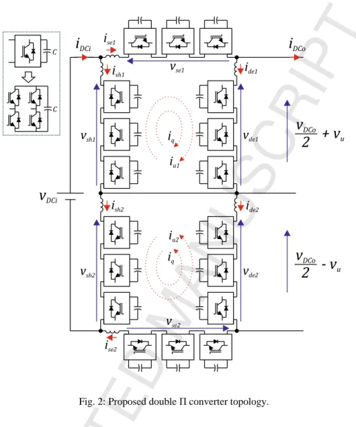
(6) The strategy for regulating the H-bridge converter DC link voltage of the proposed DC-DC converter is a two-fold scheme: 1) control of the total energy in every branch of the DC-DC converter topology and 2) balance of the DC link voltage of every H-bridge converter module that forms a branch. In order to control the total energy in each branch of the converter topology, DC and AC circulating currents are used. These currents are imposed in the power converter by a PI and a resonant controller, respectively. As shown in Section 2, the circulating AC current. controls the total energy in the. derivation branch. This current component transfers energy to/from the DC side capacitors as given by (with. in phase). The voltage. , set by the corresponding. branch, cancels out with the AC voltage in the other П topology converter and it does not appear at the output. The currents. (i=1,2) controls the corresponding total energy in the i-th shunt branch. The. total energy in the series and derivation branches in the top and bottom П arrangements are controlled by. and. respectively.. The DC voltage balance of the N H-bridge converter modules which form a branch (i.e. the series and parallel branches) is carried out as in [15]. This is by balancing (N-1) capacitor voltage deviations with respect to the average capacitor voltage of the branch. Each voltage deviation is fed into a dedicated PI controller which sets the required balancing voltage component in each H-bridge converter module. This voltage balancing component is in quadrature to. . This facilitates design of the control system. since it provides decoupling between the energy balance and DC voltage balancing sub-systems. The inductance in series with the N H-bridges in each branch attenuates the high frequency switching current ripple generated for the H-bridges PWM strategy. The proposed topology can be used in high power applications such as HVDC conversion. For simplicity, proposals are explained using the case of N=3, as shown in Fig. 2, but they can be easily extrapolated to the general case. This paper is organized as follows: Section II describes the operating principle of the converter, the control strategy used for energy balance of each branch of the converter and the control of the H-bridge capacitor voltages. Section III shows simulation results for the complete topology and some preliminary experimental results and Section IV presents the conclusions of the work..
(7) Fig. 2: Proposed double Π converter topology. 2. Power converter control strategy Only the top half of the converter is analyzed. The bottom half operates in a similar manner, but with the output AC voltage component shifted 180º, so no AC voltage appears at the total output. In following equations upper case variables (voltages/currents) represent DC or RMS values of AC components and lowercase variables are instantaneous values. 2.1. Branch energy modelling Using the voltages and currents defined in Fig 1, it can be shown that the instantaneous power in the series, derivation and shunt branches are given by (1), (2) and (3), respectively:.
(8) (1). (2). (3). Where. ,. , and. are the instantaneous stored energy of the series, derivation and shunt. branches respectively. Average powers for the same branches are given by (4), (5) and (6), respectively:. (4). (5). (6). Where. ,. respectively.. , and and. are the average stored energy of the series, derivation and shunt branches are RMS values of. and. respectively. According to (6),. can be used. to control the total energy in the shunt branch. From (5) it can be noticed that derivation branch energy can be controlled using. . Adding (4) and (5) yields to:. (7).
(9) Therefore, the total energy in the series and derivation branch together can be controlled by adjusting. ,(. is the output current and can be considered a perturbation). Adjustment of each. current component, as described in next section, is done in according to its corresponding energy deviation, with respect to its reference value, in a closed loop fashion.. 2.2. Branches energy control strategy The control structure for the energy control in the shunt branch uses a PI controller. This sets the (see Fig. 3). Considering that the internal current loop is faster than the outer. reference current. energy loop, then a simple second order system with unity feedback, reflecting the first order system in (6) with a frequency. gain plus the controller, is used. For a given damping factor. is and natural. , the controller parameters for shunt energy control loop are given by:. (8). This current. is then forced by the shunt branch using an internal current control loop, as depicted. in Fig. 3. For designing the controller, a closed loop containing a PI controller, a first order plant corresponding to the branch inductance L and its internal resistance R, and a low pass current filter with a cutoff frequency. in the feedback path (set to 50Hz) is considered. For a given damping. factor is and closed loop natural frequency. , the controller parameters are given by:. (9). The strategy for the energy control in the derivation branch also uses a PI controller, see Fig. 4, which sets the RMS current. . This RMS current. obtain the circulating reference current. is multiplied by a 100 Hz template sinusoidal signal to. .This current component is forced through the converter by. an internal current control which uses a resonant controller. A second order control loop, similar to the shunt energy controller is used, considering the PI controller with first order system in (5). Note that. gain in the forward path and the. is considered as a disturbance. For a given.
(10) damping factor. is and natural frequency. , the controller parameters for derivation energy. control loop are given by:. (10). The choice of the frequency for the compensation AC voltage component is a trade-off between converter losses and capacitor requirements, measured in terms of energy storage, hence physical size of capacitors. The higher the frequency of the AC component, the higher the switching losses, hence converter losses, but the smaller the change of energy of DC link capacitors during one cycle of the AC compensation voltage. Assuming H-bridge modules use medium voltage IGBTs, targeted for a few kilohertz of switching frequency; it has been thought that a good compromise between power losses and capacitor size would be 100 Hz. In a real application with hundred of cells, the switching frequency will be between 3 to 5 times the circulating current frequency. In this case, compared to the case of 50 Hz applications, such as MMC based HVDC converter stations, this may increase converter losses of about 20%, but it might reduce the size of capacitors by a factor of 2 resulting in a more compact topology. The design of the resonant controller follows the approach presented in [10]. The controller has the transfer function given in (11). Parameters. and. parameters are chosen as in the case of a. standard PI controller with the branch inductance L and resistance R as a first order plant with unity feedback. This is to ensure sufficient bandwidth, or alternatively a fast enough time response, to adequately track the reference input, assumed to be a slowly varying DC signal.. (11). For a desired closed loop natural frequency. and damping factor , the parameters for the. controlled in (11) are given by (12).
(11) The controller in (11) shifts the frequency response of the standard PI by. .. Therefore, it ensures good tracking of the sinusoidal reference current component. The scheme of the resonant current controller is also depicted in Fig. 4. The total energy in the series and derivation branch is controlled by the adjustment of. (see Fig.. 5). A PI controller processes the energy error and sets this DC reference current component, which like the AC current component, is imposed in the converter by an internal current control. A closed loop system is obtained taking into account (7) with a The term. gain in the forward path and the controller.. is considered as a disturbance. For a given closed loop natural frequency. and a damping factor. , the controller parameters for the total energy control loop are given. by:. (13). 2.3. H-Bridge DC Link Voltage Balance The strategy consists on comparing (N-1) DC-Link voltages (corresponding to N-1 H bridge converter) of each branch with the average DC link voltage of that branch. A PI controller processes the error and generates the RMS voltage magnitude of the voltage balance component, sinusoidal voltage balance,. , is obtained by multiplying the PI output by a 100 Hz template. sinusoidal signal which is 90° shifted from. . The. energy required for voltage balancing is transferred. from/to the H-Bridge module by forcing a constant amplitude 100 Hz sinusoidal current in phase with. . Therefore,. . A. is 90° out of phase with respect to. which is. and does not affect branch. energy balance. For the case considered here (N=3), two PI controllers are needed to process the voltage error of two capacitor voltage, respect to the average value of the three capacitor voltages. This sets the voltage balance component for two H-bridge modules. The voltage balance for the third H-bridge,. , is obtained as: (14).
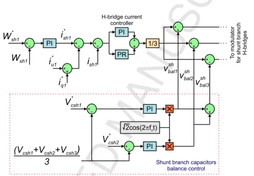
(12) Each PI output is the RMS voltage unitary signal at 100 Hz and results in thus determined by. (with. (in this case i=1,2). This voltage magnitude is shaped by a . The energy transfer for balancing in each DC-Link is and. in phase).. A resonant controller controls the total circulating current. through the converter. The. resulting current is the reference to the resonant controller and it is forced by the series branch. Fig. 3 shows a schematic for the energy control and DC-link voltage balance strategy for the shunt branch.. Fig. 3: Schematic for the shunt branch energy control and DC Link voltage balance control loops.. Fig. 4 shows a schematic for the derivation branch energy control and DC-link voltage balance strategy in this branch..
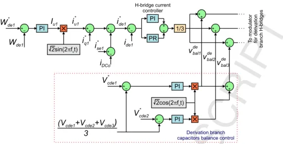
(13) Fig. 4: Schematic for the derivation branch energy control and DC Link voltage balance control loops.. Fig. 5 shows a schematic for the total series and derivation branch energy control. The DC link voltage balance for the series branch is also depicted in Fig. 5.. Fig. 5: Schematic for the total (series and derivation branches) energy control and series branch DC Link voltage balance control loops..
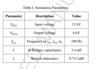
(14) 3. Results The system has been simulated and tested under load impact and step increase in output voltages, to demonstrate the feasibility of the energy control in all branches and the voltage balance mechanism with each branch. Preliminary experimental results are also shown. 3.1 Simulation results The proposed converter has been fully simulated using PSIM platform. Simulation parameters are shown in Table I. It is assumed that the proposed topology could be implemented using the 4500V, 1200A, Infineon FZ1200R45KL3_B5 IGBT. The DC link voltage in each cell is set to 2.5kV. The branch maximum DC current is 0.33 kA and peak AC current is 0.67 kA, yielding to a 4MW rated power. Table I. Simulation Parameters Parameter. Description. Value. Input voltage. 12 kV. Output voltage. 6 kV. Frequency of C. 100 Hz. H-Bridges capacitance. 3.4 mF. Branch inductance. 0.713 mH. Fig. 6 and 7 illustrates the dynamic performance of the voltage balance strategy for top and bottom Π converters respectively. Initially, capacitors are pre-charged to different values so they exhibit a noticeable unbalance. The voltage balance strategy is enable at t=0.1s. As seen in Fig. 6 and 7, capacitors voltages equalize within 0.4 s and then remain well balanced. As can be seen, in each branch, capacitor voltages are balanced and close to the reference value of 2.5 kV. The final steady state voltage depends on the energy settings. This result demonstrates the effectiveness of the energy balance and voltage balancing control strategies..
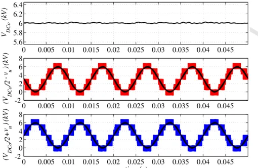
(15) Fig. 6: DC-links voltages balance performance for top Π converter: shunt branch (top), series branch (middle) and derivation branch (bottom).. Fig. 7: DC-links voltages balance performance for bottom Π converter: shunt branch (top), series branch (middle) and derivation branch (bottom). Fig. 8 shows the output voltages for the top and bottom Π converter topologies and the total converter output voltage. . The alternating component can be clearly noticed in Fig. 8a and Fig. 8b, because. of the 100Hz frequency of the output.. . In the double П topology (Fig. 8c) this AC component cancels out from.
(16) Fig. 8: Output voltage from: top Π converter (top), bottom Π converter (middle) and double Π converter (bottom). The performance of the converter topology control strategy has also been tested for an output load impact. Initially the converter is supplying 50% of rated power and the load is increased to 100% at t=0.1s, Fig. 9 shows that there is only a small disturbance on the output voltage limited to less than 1.2%. Input voltage and input and output current are also shown. Because of the voltage ratio chosen for the topology, the input current is about 50% of the output current.. Fig. 9: Input and output voltage (top) and input and output current (bottom) for a load impact. Capacitors voltages of all H-bridges, for top and bottom Π converters, are shown in Fig. 10 and 11 respectively for the load impact described above. The results show that deviation from the reference in.
(17) all capacitor voltages is driven to zero under the action of the energy control mechanism. The voltage ripple remains within 10%.. Fig. 10: Capacitors voltages (top Π converter) for a load impact at t=2 s. DC Links for: shunt branch (top), series branch (middle) and derivation branch (bottom).. Fig. 11: Capacitors voltages (bottom Π converter) for a load impact at t=2 s. DC Links for: shunt branch (top), series branch (middle) and derivation branch (bottom)..
(18) The energy for the shunt, series and derivation branches, under the load impact, is shown in Figures 12. The energy reference for every branche is set to 31.88 [kJ], which corresponds to DC link voltages of 2.5kV for each H-Bridge module. The energy is calculated as. , where. is the i-th. DC link voltage in a given branch. The graphics for top Π converter are shown in red where as the one for the bottom Π converter is shown in blue.. Fig: 12: Energy for top (red) and bottom (blue) Π converters for: shunt branch (top), series branch (middle) and derivation branch (bottom). Fig. 13 shows the steady state currents in each branch for the top Π converter after the load impact. The steady state currents for the bottom converter are similar. The total current in the series, shunt and derivation branches are shown..
(19) Fig. 13: Current in each branch for the top (red) and bottom (blue) Π converters: shunt branch (top), series branch (middle) and derivation branch (bottom). The current in the shunt branch does not practically exhibit any DC value, because in steady state the DC current needed to regulate the energy in that branch is practically zero. Therefore, only the circulating current (about 0.66kA peak) is present. For the series branch, apart from the circulating current, a DC current (about 0.33kA) circulates for the series branch corresponding to part of the current transfer to the load. The same is observed in the derivation branch with a DC current in the order of -0.33kA. Fig. 14 shows the performance of the system for a step increase of 20% in output voltage maintaining constant the input voltage. Initially the power delivered by the converter is 50% (2MW), after increasing the voltage the power delivered by the converter raises to about 2.88MW..
(20) Fig. 14: DC voltage performance for a 20% increase in output voltage. The current in all branches for a top and bottom Π converters are shown in Fig. 15 showing a similar performance as in Fig. 13. The current in the shunt branches mainly carries the circulating current whereas the series and derivations branches changes their currents in order to account for the increased in deliver power.. Fig. 15: Branch currents for the top (red) and bottom (blue) Π converters for a 20% increase in output voltage: shunt branch (top), series branch (middle) and derivation branch (bottom).. Fig. 16 shows the voltage balancing mechanism performance for the step inverse in output voltage described above. The effect of the step increase in output voltage is mainly reflected in the capacitor.
(21) voltages in the series and derivation branches, but the balancing mechanism equalizes all voltages in less than 0.2s.. Fig. 16: Capacitor voltages in shunt (top) series (middle) and derivation (bottom) branches for a step increase in output voltage.. 3.2 Experimental results Preliminary experimental results are shown operating H bridges at 100V DC link voltage. The control platform is based on both a TMS320C6713 processor DSP board and a FPGA interface board. Data transference between the DSP board and a PC host is done using a DSK6713HPI (Host Port Interface) daughter card. The DSP bard carries out several tasks including solving control loops, communications and PWM reference generation. The FPGA board carries out data acquisition and generates the PWM signal for the H bridges. Each bridge converter uses 600V/60A IGBT and 2.2mF DC link capacitor. The switching frequency is 2 kHz. Fig. 17 shows the main components of the experimental setup, i.e., the power converter, the host PC and a detail of a power converter branch, the DSP and FPGA boards and the host PC..
(22) Fig. 17: Experimental setup.. Fig. 18 shows the top (blue) and bottom (green) derivation branch voltages, the output voltage (pink) and the load current (yellow) when the converter is supplying a resistive plus inductive load. (Voltage probes used attenuate voltage measurements by 2). The branch voltages exhibit three distinctive voltage levels with a mean value and the 100Hz components 180° out of phase. The ac peak voltage per branch is about 110V. Initially the DC voltage is about 280 and DC load current is about 5A. Both DC voltage and current are digitally filtered with a 10kHz bandwidth low pass filter. A step increase of 20%, resulting in a DC voltage of about 330V, is observed in the DC voltage with the corresponding increase in the DC load current. The DC voltage performance is in agreement with the simulation result depicted in Fig. 14.. These results demonstrate the cancellation of the 100Hz. derivation branch voltages and the performance of the the DC output voltage to step changes in reference..
(23) Fig. 18: Top (blue) and bottom (green) derivation branch Voltages, 200V/div; DC output voltage (pink), 200V/div; and load current (yellow), 5A/div.. Fig. 19 shows the top (green) and bottom (yellow) derivation branch voltages, the DC output voltage (pink), the load current (green) and top (yellow) and bottom (brown) total derivation current branches, i.e. DC and circulating currents, when the DC voltage is about 280V and the current is about 5A. As expected, the derivation branch currents contain a DC component, similar in the top and bottom branches, and ac components equal in magnitude but 180° out of phase. These results illustrate the distribution of the derivation branch currents, DC and AC components, when the output is supplying energy to a load. The slight voltage oscillations observed in the AC branch voltages are due to the oscillation in the H-bridge DC link voltages (voltage ripple). These oscillations are the result of the AC instantaneous pulsating power and its effect is more noticeable when the circulating current is at its peak value..
(24) Fig. 19: Top (blue) and bottom (green) derivation branch Voltages, 200V/div; DC output voltage (pink), 200V/div; load current (green), 10A/div; top (yellow) and bottom (brown) derivation branch currents, 10A/div .. 4. Conclusions This paper has introduced a novel Modular Multi-Level Converter topology for DC-DC converters. The proposed topology does not require the use of high frequency, high voltage transformers. A suitable control strategy has been proposed for the aforementioned DC-DC converter, for both the arm energy control and module capacitor balance. The proposed control strategy is based on outer energy loops that make use of orthogonal current components to control the branch energy. The obtained branch currents are imposed on each branch by means of PI or P+R controllers. The technical viability of the proposed MMC DC-DC converter and control strategy has been thoroughly validated by means of detailed PSIM simulations. The proposed capacitor balancing mechanism has been thoroughly validated. Moreover, the complete system has been validated during.
(25) start-up, steady state and load impact operation. Preliminary experimental results obtained from a small power prototype have also been shown. Acknowledgements This work was supported by Fondecyt grant 1151325, CONICYT/FONDAP/15110019, The Spanish Ministry of Economy and EU FEDER funds under grant DPI2014-53245-R, The University of Magallanes grant PR-FI-02IE14/15, Universitat Jaume I grant P1.1B2013-51, the Newton Picarte Project EPSRC:EP/N004043/1 and CONICYT DPI20140007. References [1] H. Akagi, Classification, Terminology, and Application of the Modular Multilevel Cascade Converter (MMCC), IEEE Trans. Power Electronics, 36 (2011) 3119-3130. [2] A. Antonopoulos, L. Angquist, H.P. Nee, On dynamics and voltage control of the Modular Multilevel Converter, EPE 2009. [3] C. D. Barker, C. C. Davidson, D. R. Trainer, R. S. Whitehouse, Requirements of DC-DC converters to facilitate large DC grids, Cigre, SC B4 HVDC Power Electron., 2012. [4] 4465.. J. A. Ferreira, The Multilevel Modular DC Converter, IEEE Trans. Power Electronics, 28 (2013), 4460-. [5] N. Flourentzou, V. G. Agelidis, G. D. Demetriades, VSC-based HVDC power transmission systems: An overview, IEEE Trans. Power Electronics, 24 (2009), 592-602. [6] M. Hagiwara, H. Akagi, Control and Experiment of Pulsewidth Modular Multilevel Converters, IEEE Trans. Power Electronics, 24 (2009), 1737-1746. [7] D. Jovcic, B. T. Ooi, Developing DC transmission network using DC transformers, IEEE Trans. Power Delivery, 25 (2010), 2535-2543. [8] S. Kenzelmann, A. Rufer, M. Vasiladiotis, D. Dujic, F. Canales, Y. R. de Novaes, A versatile DC-DC converter for energy collection and distribution using the Modular Multilevel Converter, EPE 2011, 1 –10. [9] A. Lesnicar, R. Marquardt, An Innovative Modular Multilevel Converter Topology Suitable for a Wide Power Range, IEEE Power Tech Conf., June 23-26, 2003. [10] P. Lezana, C. Silva, J. Rodriguez, M. Perez, Zero Steady State Error Input Current Controller for Regenerative Multilevel Converters Based on Single-Phase Cells, IEEE Trans. Ind. Electronics, 54 (2007), 733740. [11] T. Luth , M.M.C. Merlin , T.C. Green, F. Hassan , C.D. Barker , High-Frequency Operation of a DC/AC/DC System for HVDC Applications , IEEE Trans. Power Electronics, 29 (2014) , 4107 – 4115. [12] D. Montesinos-Miracle, M. Massot-Campos, J. Bergas-Jane, S. Galceran-Arellano, A. Rufer, Design and Control of a Modular Multilevel DC/DC Converter for Regenerative Applications, IEEE Trans. Power Electronics, 28 (2013), 3970-3979. [13] S. Norrga, L. Angquist, A. Antonopoulos, The polyphase cascaded-cell DC/DC converter, Energy Convers. Congr. Expo. ECCE IEEE, (2013) 4082 – 4088. [14] M. Saeedifard, R. Iravani, Dynamic performance of a modular multilevel back-to-back HVDC system, IEEE Trans. Power Delivery, 25 (2010), 2903–2912. [15] D. Soto-Sanchez, R. Pena, R. Cardenas, J. Clare, P. Wheeler, A Cascade Multilevel Frequency Changing Converter for High Power Applications, IEEE Trans. Ind. Electronics, 60 (2013), 2118-2130. [16] T. Westerweller, A. Orioni, D. Parquet, S. Wehn, Trans Bay Cable- world’s first HVDC system using multilevel voltage-source converter, CIGRE Paper B4-101, Paris, 2010..
(26)
Figure
+7


Documento similar