Abstract—This work presents a new methodology for modeling, design and implementation of power amplifiers in different technologies. As result of comparison, a flowchart with a new methodology is proposed which can be useful for the designer to design and implement power amplifiers with low, medium and high power devices in different technologies. This paper is divided in 4 parts: The first one is an introduction to the importance of modeling and design techniques in the final implementation of power amplifiers for the modern communication systems. The second one details the modeling process for different technologies, which final result is a unified model. The third part is related with the characterization of high power transistors, with special emphasis on substrate characterization and final implementation of a power amplifier. Finally, in the fourth part, the new methodology is proposed based on the comparisons of previous procedures.
Index Terms— microwaves, modeling, power amplifier, substrate.
I. INTRODUCTION
Modern communication systems require RF power amplifiers to operate with large signal in
broadband conditions. For 5G systems, requirements will be more demanding; and different
technologies such as GaN and LDMOS are currently under investigation. Those two technologies
have improved power density compared with traditional compounds semiconductors [1]. It originates
problems with power dissipation which creates dispersion and thermal effects [2]. Consequently, for
the design of RF power amplifiers using these semiconductors, it is essential to use accurate models
that take into account these phenomena. Furthermore, for power amplifier implementation, an
accurate substrate characterization is required, in order to get the appropriate input and output
impedances for the matching networks. In this paper we will show that through the use of models
flexible enough to predict static and dynamic conditions, and a one-port substrate characterization
technique, we can demonstrate that it is possible to implement efficiently RF power amplifiers in
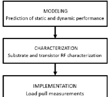
LDMOS technologies. Based on those steps we propose a new methodology which is summarized in
Fig. 1. That methodology will be explained in the following sections.
New methodology for modeling, design and
implementation of RF power amplifiers
Guillermo Rafael-Valdivia, Omar Castellanos Ballesteros.
Fig. 1. Flow chart of the proposed methodology for the power amplifier design.
II. MODELING
Modern communication systems, such us internet of things (IoT) and 5G are currently under
investigation; however they will demand the use of different technologies for amplifiers. For instance
GaAs is a promising technology for low power and linear applications; and GaN / LDMOS for high
power amplifiers for long distance communications. As these 2 technologies behave differently, it
makes sense to consider different strategies for modeling. However despite their differences, there are
some common characteristics. One of them is the output conductance (gds) and transconductance
(gm) frequency dispersion, considered as one of the causes for the memory effects which cause
complexity in linearization [3]. In this paper we will call this effect “the frequency dispersion
phenomena”. We characterized this effect through I/V pulsed measurements by using the DIVA
system provided by Accent Technologies [4]. The measurements were carried out in University
College Dublin in the RF and microwave group. As it is shown in Fig. 2, DIVA system is a 2 port
equipment, which is able to send and read pulsed voltages in the drain and gate side of a microwave
transistor placed in a specific test fixture.
In Fig. 3 it is shown the RF signal sent by DIVA which has a pulse width of 0.2usec with a period
about 1ms. This duty cycle allows to measure only the dynamic behavior by keeping the same bias
point. The system can measure the static (DC) characteristics of any device and compare them with
the dynamic (pulsed) characteristics.
Fig. 3. Voltage waveform at the drain side of a transistor, provided by the DIVA pulsed measurement test system.
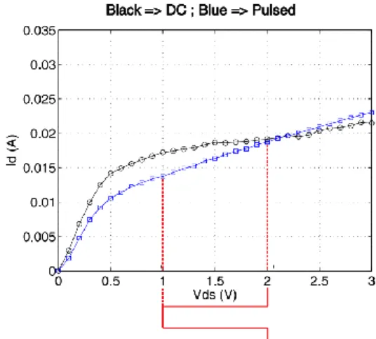
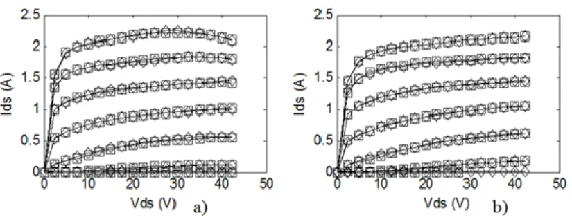
For a NE76038 GaAs low power HEMT, the evidence of the frequency dispersion effect is shown
in Fig. 4. We can see difference in the slopes of the IV curves for the static and dynamic conditions.
[5]. Furthermore it is possible to set different DC bias points (multibias) and perform pulsed
measurements for each case. In this scenario there are also differences between each of the pulsed
characteristics. It means that the difference in the slopes are due not only to the bias points positions;
but also to the trapping effects as it is indicated in Fig. 5.
Fig. 4. DC and Pulsed IV characteristics for the NE76038 GaAs HEMT device.
In order to demonstrate that by using only a single non linear Ids equation we can predict all of
these effects, we used the technique proposed in [4]. In that technique we demonstrated that by using
COBRA model [6] we could predict the DC measurements. However in order to include in that model
Ri
effective voltages equations are shown in (1) and (2), where vdse and vgse are the effective voltages,
dvd and dvg are the pulsed voltages, and ki are fitting parameters.
The pulsed voltages are extracted from the large signal equivalent circuit by using a four-terminal
topology which is shown in Fig. 6.
0 0.5 1 1.5 2 2.5 3
Fig. 5. Plot of the measured (diamonds) and modeled (squares) pulsed drain to source current obtained for the NE76038 with the proposed technique. Pulse width 0.2μsec and duty cycle: 0.02%. Extrinsic applied voltages: a) VgsDC=0V, VdsDC=0.5V;
b) VgsDC=-1V, VdsDC=0.5V; c) VgsDC=0V, VdsDC=3V; d) VgsDC=-1V, VdsDC=3V. Sweep in gate voltage: 0V to -1V
(uniform step). Similar accuracy was obtained in multibias conditions. [4]
freq (1.000GHz to 10.00GHz)
nonlinear equation for Ids. Results are shown in Fig. 7.
Fig. 7.Measured (diamonds) and modeled (squares) pulsed Ids obtained @ VgsDC=-4V, VdsDC=40V for the CGH40010F
10W HEMT transistor. a) Pulse width: 30µsec. b) Pulse width: 5µsec.
One of the properties of this model is that it can be used to model the RF performance. In Fig. 8 it is
shown the difference between modeled and measured S-parameters. Furthermore, with the complete
characterization of the device, the proposed model can be used to predict the output power vs input
power behavior as it is shown in Fig. 9.
Fig. 8. Measured (circles) and modeled (lines) S-parameters for the NE76038 using the proposed method. Extrinsic applied voltages: VdsDC=3V; VgsDC=0V. Similar agreement was obtained in multibias conditions and for other S-parameters.
Fig. 9. Large signal two tone output power performance centered at 2GHz and tone spacing of 4MHz at VdsDC=2V and
In conclusion for this section, we can say that despite the different non-linear equations for Ids used
for the GaAs and GaN devices (COBRA and Angelov respectively), the same methodology for
modeling was used and validated. This methodology provided us coherent predictions for the static
and dynamic behavior for both technologies.
III. SUBSTRATE CHARACTERIZATION AND POWER AMPLIFIER IMPLEMENTATION
After finishing the modeling process, we focus on the substrate characterization and the power
amplifier implementation procedures. Both of them have been carried out in our university. In this
section we will demonstrate that it is possible to build power amplifiers according to specific target
specs using low cost equipment but well stablished models. Finally we will compare the results with
the ones shown in datasheets showing coherence.
A. Substrate characterization
Before to do the design and implementation of an amplifier, the designer requires to know the
dielectric constant and loss tangent values of the substrate to be used. Normally the designer uses the
values provided in the datasheets which are average values dependent on the fabrication process.
However, when the complexity of the circuit requires high accuracy, substrate characterization is a
must. (i.e. power amplifiers in microwave ranges). Several methods have been proposed to measure
the fundamental properties of substrates. Some of them are based on physical measurements in low
frequencies using the relationship between the capacitance of a dielectric, the permittivity and the
thickness of the dielectric [7]. However their accuracy is not enough for high frequency conditions
(GHz range). Furthermore with that kind of methods is not possible to get loss tangent values. In [8],
the methods for measuring permittivity are summarized in 2 categories: resonant and non-resonant. In
some telecommunications companies, such as Freescale Semiconductors (now NXP), according to the
professional experience of the author, the resonant two-port characterization technique is mainly used
for power amplifier design. This technique is based on the measurements of scattering parameters,
specifically the transmission parameter S21. That method allows the measurement of the transmission
coefficient at resonant frequencies in order to use those results as reference values, in order to find the dielectric constant (ε) and losses (tan δ) through optimization procedures performed by CAD tools.
This method is accurate enough; but it requires the use of a 2 port equipment such a Vector Network
Analyzer (VNA), which sometimes is not available in public universities in our country. In this
section, we will show that using only return loss measurements in a single port configuration it is
possible to characterize substrates with accuracy in the microwave range. The advantage of this
technique is its simplicity and accuracy. Furthermore, in environments with lack of resources, it is a
low cost solution because the use of VNA is not required. The proposed method in this paper for
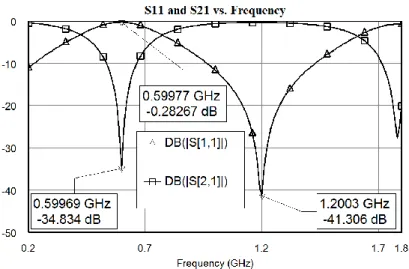
10. We used as test vehicle the low cost FR-4 substrate. The shunt stub is a quarter wave length line at
a specific design frequency. It presents a variable impedance to the access ports. So, according to the
frequency of the excitation signal, the impedance of the stub can change from open to short. So we
will have minimum or maximum values of S11 and S21 at specific resonant frequencies. In our design
we decided to set the first resonance frequency at 600MHz (design frequency). We have selected that
value considering that its second harmonic must be within the frequency range of our spectrum
analyzer (HP8591A). Previous to the measurements, we compared the behavior of the simulated S11
and S21 for our resonator as it is shown in Fig 11.
MLIN
Fig. 10.Proposed resonator topology for substrate characterization. Port 2 can be connected to a 30dB attenuator.
In Fig. 11 it is possible to appreciate that for the conventional method (S21 measured with VNA)
the first local minimum of S21 is at the design frequency (600MHz). However for the proposed
method (S11 measured only with a spectrum analyzer and a coupler), the first local minimum of S11
is at the second harmonic (1200MHz). We have verified by using the optimization tools of AWR
(Microwave Office), that variations on ε are responsible for shifting the resonant frequency
(horizontal variation in local minimum of S11), while tuning on tan δ have direct impact to determine
how deep is the resonance valley in S11 (vertical offset). The influence of the optimization of the
dielectric constant and the loss tangent are independent (they don’t impact to each other). Consequently, through an optimization of ε and tan δ it is possible to fit S11 simulations with S11
measurements, so it is possible to find the actual value of the substrate parameters. In Fig. 11 it is
possible to see that an advantage of the proposed 1-port method, over the conventional one, is the
presence of a local maximum, located at the central frequency fc (close to 0.6GHz). This point is used
Fig. 11. Comparison between the behavior of simulated S11 and S22 for substrate characterization purposes
To perform the measurements, the setup shown in Fig.12 was implemented, where SUT is the
substrate under test; Pref represents the reflected power; Pinc the incident power; Pmeas represents
the measured power; CF represents the coupling factor; and RL the return loss.
Fig. 12. Block diagram of the proposed method for the 1-port substrate characterization.
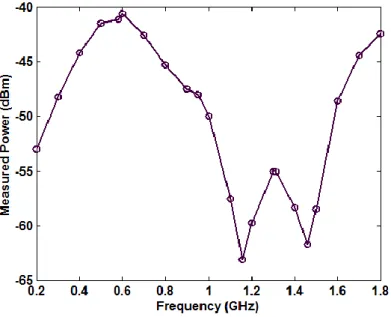
The coupling factor and insertion loss were measured in the frequencies of interest. A Rohde and
Schwarz RF (SMT06) signal generator has been programmed in frequency sweep mode from
200MHz until 1.8GHz, covering the previously defined central frequency (fc) and its second
harmonic. Those values are within the range of operation of the Spectrum Analyzer HP8591A. As it is
shown in Fig. 13, experimentally we have seen the resonant frequency of Pmed at 1158MHz.
Furthermore, there is a maximum at 579MHz. Both of them are a clear effect of the substrate
(resonator) connected to the setup. The second minimum shown in Fig. 13 at 1455 MHz, is due to the
cutoff frequency of the coupler. From those results, the return loss of the substrate under test is
(3)
Fig. 13.Measured power (Pmeas or Pmed), using the setup shown in Fig. 12.
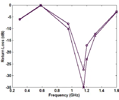
Consequently, those values of Return Loss (RL) can be compared with simulated results, as shown
in figure 14. Considering that the geometrical tolerance in the implementation of the circuit
(dimension of the lines) is accurate enough, the difference between measurements and simulations is
only due to the physical parameters of the substrate: ε and tan δ.
From initial simulations in Microwave Office, the maximum was located at 600MHz and the
minimum at 1200 MHz. So, the parameter ε was optimized in simulations, shifting the resonance
frequency until the peak reaches the measured value: 1158MHz. By doing this, the position of the
local maxima was automatically placed at its measured value: 579MHz, confirming the coherence of
the method. Once the frequencies were aligned, we had to deal with the magnitude values of return loss. To do this, tan δ was optimized fitting the local maximum magnitude. It is important to remark
that doing this second optimization, there is no impact in the position of the resonant frequencies. The
differences in the deep zone of the curves are expected, and are due to the low magnitude of measured
Fig. 14. Simulated (x) and measured (o) return loss for the substrate under test.
After the optimization process, we got ε= 4.4 and tan δ = 0.02. The average values for these
parameters, indicated in [9] are: ε = 4.7 and tan δ =0.014. Those values are also coherent with the
ones indicated in [10]. In order to confirm the validity of the proposed method, simulations in ADS
were performed as well. The results obtained are coherent with the ones that we got through
optimization in Microwave Office. The same characterization process was performed with the RF35 substrate; we got ε= 3.5 and tan δ = 0.002. The thickness of the substrate was 20 mils (0.5mm). The
average values for these parameters, indicated in [11] are: ε = 3.5 and tan δ =0.0018. Fig. 15 shows
the resonator implemented to characterize the RF-35 substrate.
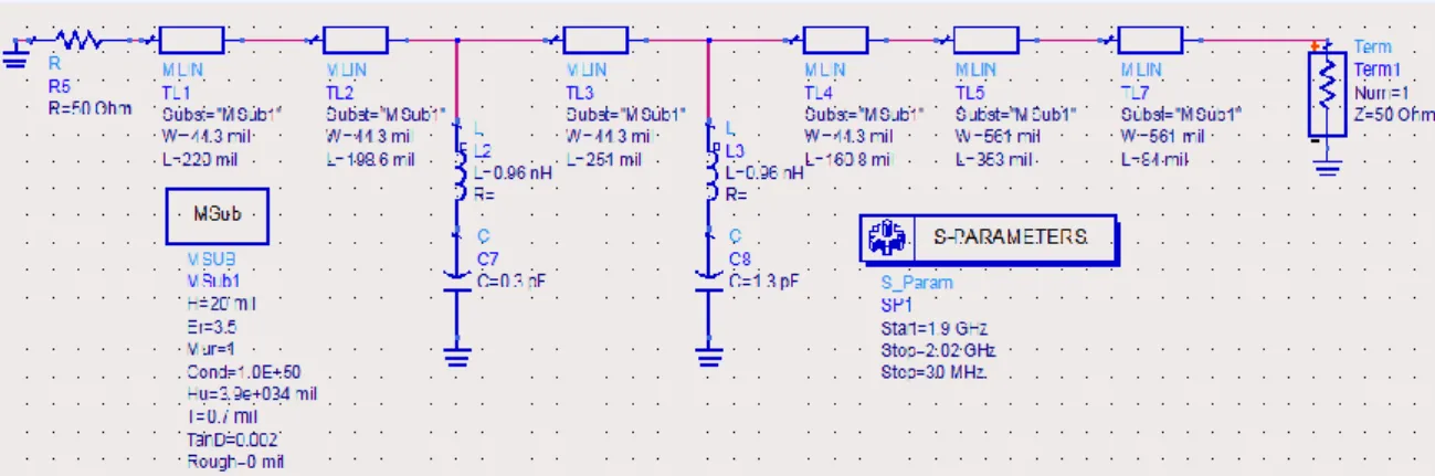
B. Power Amplifier Implementation
We built a power amplifier using the MRF6S18100 LDMOS device from Freescale
Semiconductors (now NXP). We used the RF35 substrate previously characterized with the
parameters and dimensions shown in the previous paragraph. According to its datasheet given in [12],
this field effect transistor was designed for base station applications, from 1800 to 2000MHz with
100Watts output power and 15dB gain (at P1dB conditions). The recommended bias point for this
device is VDD = 28 Volts (typical for LDMOS) at IDQ = 900mA (class AB). In contrast to the
conventional bias tee configuration with discrete inductance and capacitors, the bias network in our
design uses a quarter wavelength line with a shunt cap in order to provide a virtual RF short circuit at
a quarter wave distance from the drain terminal of the transistor. Similar procedure was used to bias
the gate side. For both cases we used symmetrical feeders in order to improve bandwidth. Simulations
of the bias network design are shown in Fig. 16.
Fig. 16. Bias network simulations for the power amplifier based on the MRF6S18100 LDMOS device.
For the design process of the matching networks, instead of using the conventional lumped or
discrete matching narrow band techniques optimized only for power or gain; we used wideband
techniques with the combination of lumped and discrete components, in order to take advantage of the
best properties of each technique. The goal of those networks are to allow the transistor to see the
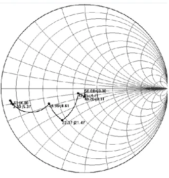
same impedances shown in the load pull data, depicted in Fig.17 in order to meet the target specs
(best trade-off between power, efficiency and linearity).
The input and output matching networks are shown in Figs. 18 and 19 respectively, in which the
bypass capacitor (modeled as a capacitor in series with a parasitic inductance of 0.9nH) is not shown
for visualization purposes of the trajectory of the impedances (Fig. 20 and 21). Its effect is small
because it acts like a short circuit at the central frequency. Furthermore, we can see that the
impedances obtained in our design (Table I) are similar to the ones provided by the data sheet.
Fig. 18Input matching network for the power amplifier based on the MRF6S18100 LDMOS device.
Fig. 20.Trajectory of the impedances for the input matching network for the power amplifier based on the MRF6S18100 LDMOS device.
TABLE I.SOURCE AND LOAD IMPEDANCES OBTAINED FOR THE FINAL POWER AMPLIFIER DESIGNED WITH THE MRF6S18100 LDMOS DEVICE
Frequency (MHz) Zsource (ohms) Zload (ohms)
1900 2.68-j4.33 1.48-j3.25 1930 2,65-j4,18 1.51-j3.13 1960 2,64-j4,02 1.54-j3.03 1990 2,63-j3,87 1.55-j2.95 2020 2,62-j3,72 1.56-j2.87
To test the performance of our amplifier in different conditions, we performed a power sweep test
in three different frequencies in order to extract the gain and capture the output power at P1dB
conditions. Our system calculates the gain from every measured power. It stops when the calculated
gain compresses 1dB. This allow us to capture the output power at P1dB, whose values are shown in
Table II. We selected 3 frequencies: 1930, 1960 and 1990MHz, because this is the frequency band
indicated in the data sheet of our transistor [12] (page 1) for its specific application. By doing that, we
characterized the amplifier in the edges and in its central frequency. As it is shown in Table II, the
obtained values of those parameters agree with the values indicated in the data sheet for the targeted
frequency band.
TABLE II.POWER SWEEP MEASUREMENTS FOR THE FINAL POWER AMPLIFIER DESIGNED WITH THE MRF6S18100LDMOS DEVICE
Freq(MHz) G(dB) Pin(dBm) Pout(dBm) Pout(W) IRL(dB)
1930.00 14.56 37.00 50.53 113.06 -18.34 1960.00 14.66 37.01 50.66 116.36 -30.37 1990.00 14.67 36.96 50.63 115.57 -16.41
The measured average gain and ripple were 14.63dB and 0.11dB respectively. Finally we
performed a frequency sweep test in small signal conditions (1CW) in order to obtain the global
behavior of the amplifier. As it is shown in Fig. 22, we got less than 0.2 dB gain flatness from 1930
MHz until 2000 MHz, with IRL values better than -14.5dB. The final implemented amplifier is shown
in Fig. 23. The transistor is in the middle of the PCB. This device has been measured with plastic
pushers attached with screws (not shown in the picture) in order to avoid soldering and to test the
Fig. 22.Frequency sweep measurements for the MRF6S18100 LDMOS device.
Fig. 23.Final prototype: implemented power amplifier using the MRF6S18100 LDMOS device.
IV. CONCLUSIONS
In this paper we presented a methodology for modeling, design and implementation of amplifiers in
different technologies. The first step is the modeling process, in which we used effective voltage
equations to model both static and dynamic performance of the devices in multibias conditions. The
advantage of this technique is that we can embed those equations into any conventional model such as
COBRA, Angelov, Materka, Curtice, ROOT, MET, etc; and it is valid for different technologies such
as GaAs, GaN, LDMOS, etc. In fact, beginning from static measurements (DC) we can set specific
microwave transistor. After that, by doing S-parameters measurements we can see the RF
performance of the model which can be optimized in order to predict the gm/gds dispersion effect.
The second step is the substrate characterization in order to get accurate values for dielectric
constant and loss tangent. In this case we demonstrated that we can measure them by using only
1-port measurement and low cost equipment, while traditional methods uses 2 1-port measurements and
VNAs. Finally, we designed a LDMOS power amplifier by using loadpull data, in a RF35 substrate
previously characterized. By using symmetrical bias networks and lumped/discrete element
combinations for the matching networks, we demonstrated that we can reach the appropriate
impedances and satisfy the power and gain specs.
ACKNOWLEDGMENT
The authors thank Dr. Apolinar Reynoso- Hernández from CICESE (México) for the measurements
on the GaN device. The authors also thank the design team and modeling team of Freescale
Semiconductors, Toulouse, France (now NXP) for his valuable support with the LDMOS device.
REFERENCES
[1] Lan and al., “High power density InGaP PHEMTs for 26V operation”, 2005 IEEE RFIC Symp. Digest.
[2] GaN HEMT equivalent circuit model with novel approach to dispersion modelling. Justin B. King; Thomas J. Brazil. 2012 7th European Microwave Integrated Circuit Conferenc
[3] Parker1 A. E. Parker, and J.G. Rathmell, “Bias and frequency dependence of FET characteristics,” IEEE Trans. Microwave Theory and Tech., vol. 51, no.2, pp. 558-592, December 1997
[4] Single function drain current model for MESFET/HEMT devices including pulsed dynamic behavior. Guillermo Rafael-Valdivia; Ronan Brady; Thomas J. Brazil. 2006 IEEE MTT-S International Microwave Symposium Digest [5] IMOC Nonlinear device model for GaN and GaAs microwave transistors including memory effects. G.
Rafael-Valdivia, Anthony Urquizo, Thalia Mendoza. Silvio E. Barbin 2015 SBMO/IEEE MTT-S International Microwave and Optoelectronics Conference (IMOC)
[6] Improved prediction of the intermodulation distortion characteristics of MESFETs and PHEMTs via a robust nonlinear device model. V. I. Cojocaru; T. J. Brazil.1998 IEEE MTT-S International Microwave Symposium Digest
[7] Basque Country University. Physics of Materials Department. "Impedancia. Permitividad eléctrica". Available: http://www.sc.ehu.es/sqwpolim/FISICAII/P2.pdf
[8] JMOE Non-resonant permittivity measurement methods. Sergio L. S. Severo, Álvaro A. A. de Salles; Bruno Nervis, Braian K. Zanini. Journal of Microwaves, Optoelectronics and Electromagnetic Applications, Vol. 16, No. 1, March 2017
[9] "FR4" Available: http://www.farnell.com/datasheets/1644697.pdf
![Fig. 17. Source and load impedances extracted from load pull measurements for the MRF6S18100 LDMOS device [12].](https://thumb-us.123doks.com/thumbv2/123dok_es/4997529.696949/11.892.120.757.471.681/fig-source-load-impedances-extracted-measurements-ldmos-device.webp)