Abstract— A system of two coupled oscillators based on nonlinear transmission lines (NLTL) is proposed for pulsed-shaping applications. The maximum propagation frequency through the NLTL is calculated and optimized with a realistic numerical method. With additional design considerations, this is used to increase the waveform steepening capabilities of the NLTL and obtain an oscillator based on the shockwave concept. Coupling two of these oscillators with slightly different characteristics various pulse shapes can be achieved through composition of the individual waveforms. The coupled-system behavior is understood with the aid of a new reduced-order formulation, which takes into account the differences between the oscillator elements. The formulation is extended for stability and phase-noise analysis. It provides valuable insight into the impact of the individual oscillator characteristics on the coupled-system dominant poles and unsymmetrical stable phase-shift range. It also explains the variation of the spectral density with the phase shift, as well as the mechanisms for the phase noise corners observed when increasing the offset frequency. A more realistic analysis of the coupled system is also carried out with the conversion-matrix approach, using cyclostationary noise sources. The analysis and design techniques have been applied to several prototypes at 0.8 GHz.
Index Terms— Nonlinear transmission line, oscillator, stability, phase noise.
I. INTRODUCTION
O
scillators generating a periodic train of short-duration pulses can be used in high speed sampling of rapidly varying signals [1] and time domain metrology, for high speed sampling oscilloscopes and reflectometry [2]. Due to their high harmonic generation capability, they can also be applied in frequency synthesis. They enable the implementation of comb generators [3,4] providing harmonic signals spanning through a broad spectrum, often used for the calibration of test sites and instruments [4]. In addition, several impulse-radio ultrawideband transmitters at pulse repetition rates above 1 Gbps have been reported in the literature [5,6], withManuscript received July 01, 2014; revised September 11, 2014, accepted October 18, 2014. This work was supported by the Spanish Ministry of Science and Innovation under project TEC2011-29264-C03-01. This paper is an expanded version from the IEEE International Microwave Symposium, Tampa Bay, FL, USA, June 1-6 2014.
M. Pontón and A. Suárez are with the Departamento de Ingeniería de Comunicaciones, Universidad de Cantabria, Santander, 39005, Spain (e-mail: [email protected]; [email protected]).
monocycle pulses having the advantage of containing less power in the dc and low-frequency bands that cannot be radiated through antenna [7,8].
T
he pulse shaping can be achieved using nonlinear transmission lines (NLTL) [9-11], which are composed by inductor–varactor cells, where the capacitance c(v) decreases with increasing voltage v. Due to this voltage dependence the high-voltage parts of the waveform will propagate faster through the NLTL than the low-voltage ones [9-11]. The pulse shaping is generally based on soliton formation [9-10], which requires a balance between the nonlinearity due to the varactor diodes and the dispersion inherent to the discrete nature of the NLTL [9]. The soliton is a solitary wave that maintains its shape while travelling through the NLTL at a constant speed [9]. Some previous works [1], [12-16] have demonstrated the possibility to obtain an autonomous soliton generator by suitably loading an active element with an NLTL (reflection configuration) [14-15] or by using the NLTL as the feedback block of an amplifier [1, 16]. This provides a periodic pulsed waveform, with no need of an input periodic signal. Here the pulsed waveform oscillator is obtained in a different manner, making use of the shockwave concept [9, 17], together with reflection and delay effects [18]. In an ideal continuous medium, the nonlinear capacitance would lead to the formation of a shockwave when the high– amplitude section of the waveform overtakes the bottom [9], which would ideally give rise to an infinite slope, as described in [18]. In practice, the NLTL is a lossy and dispersive network, the latter due its discrete nature, and this will limit the maximum propagation frequency. The NLTL does not admit an analytical solution and approximate expressions for the Bragg frequency have been provided [10, 11], assuming equal minima and maxima of the voltage waveform across the NLTL cells. Here an efficient numerical method is presented for a realistic determination of the maximum propagation frequency fmax through an NLTL with a relatively small number of cells, under sinusoidal excitation The method, intended for harmonic balance (HB) simulators, is based on a direct calculation of the input frequency at which a specified value of insertion loss is obtained. Driving the NLTL at an input frequency sufficiently below fmax, the nonlinear operation of the diodes will lead to progressive wavefront compression, and a pulsed waveform can be obtained with the aid of a grounded parallel stub, through combination of reflection and delay effects. The optimized NLTL will then be used as the load of an active element (with a suitably feedback network) to obtain an oscillator at the original excitation frequency.However, the pulse forming capabilities can be substantially increased by coupling two NLTL-based oscillators with
Analysis of two coupled NLTL-based
oscillators
slightly different characteristics and adequate phase shift. Here the bias voltage of the active device in one of the oscillator elements will be varied to modify the corresponding output waveform, and the pulsed signal will be extracted in differential manner from the coupled system [19]. This methodology will allow the generation of various types of pulses, like narrow pulses and monocycle pulses with switchable polarity, which will be controlled by varying the phase shift between the oscillator elements. The idea is conceptually similar to the one presented in [2], which proposes a pulse generator using dual NLTLs with opposite polarity of the diodes. The input signal is split into two by an off-chip Wilkinson divider with one of the signals being delayed by a true time delay line before being fed into the corresponding NLTL. This work avoids the need of the power divider and has the advantage of the tunable delay, which is easily achieved by changing the phase-shift between the oscillator elements with a varactor diode.
Because the two coupled oscillators can be different, in this work a fully new reduced order formulation for a system of two coupled oscillators having different free-running frequencies, amplitudes and admittance functions is derived. It is limited to the case of weak coupling (which minimizes the nonlinear dynamic effects) and relies on models extracted from a HB simulation of the individual oscillators in free-running regime. The analysis methodology, of general application to any oscillator circuits, is different from that of the in-depth work [20], which considers two oscillators of the Van der Pol type under weak and strong coupling conditions.
The HB-based reduced-order formulation presented here will enable an understanding and anticipation of the behaviour of the coupled system in terms of synchronization frequency and phase shift variation versus the tuning parameter. A perturbation analysis of this system will provide insight into the impact of the individual oscillator characteristics on the stable phase shift range in synchronized regime. Results will be validated with a detailed circuit level analysis based on pole-zero identification [21-22]. In turn, a reduced order formulation for the noise analysis will provide valuable insight into the causes of the corner frequencies observed in the noise spectrum and the dependence of phase-noise spectral density on the phase shift φ between the oscillator elements. In a manner similar to the stability properties, for different oscillator characteristics, this spectral density will not be symmetrical about φ = 0º.
The paper is organized as follows. Section II presents the oscillator based on the shockwave concept. Section III describes the mechanism for pulse shaping based on the coupling of two NLTL-based oscillators, as well as the new reduced-order formulation for two coupled oscillators with different characteristics. Section IV presents the stability analysis and Section V the phase noise analysis.
II. SHOCK WAVEFORM GENERATOR
A. Optimization of the NLTL
The NLTL capacitance c(v) decreases with increasing voltage, so a waveform with steepening front can propagate through the NLTL [9]. However, this effect will be physically
limited by the Bragg frequency of the NLTL and the cut-off frequency of the diodes. Under small loss resistance of these diodes, the Bragg frequency will be much lower than the cut-off frequency. Disregarding this loss resistance, a linear electrical network with a large number n of L-C cells will be initially considered, where L and C are the unit cell inductance and capacitance, respectively. The dispersion relation of this network is given by [9]: 2 4 sin2 2 LC κ ω = (1)
The parameter in the above relationship is κ =kδ , where k is the wave number and δ is the small unit cell length. From inspection of (1), the maximum propagation frequency is:
1 B f LC π = (2)
It is the Bragg frequency, or cut-off frequency of the line. As gathered from (1), at fB, the delay per cell is κ = ± . π This property will be taken into account when deriving a numerical criterion to determine the maximum propagation frequency through the NLTL. The varactor diode used in the demonstrators is a SMV1232, with the cut–off frequency
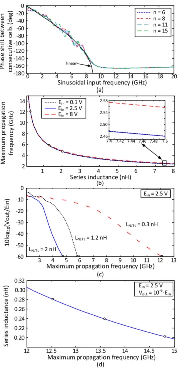
fc = 25.2 GHz. In a first stage, the propagation characteristics of the line are analyzed for various numbers n of L-C cells. The L value is 0.3 nH and the line is terminated with the approximate characteristic impedance Zc= L C/ o , where Co is the linear capacitance. In the applications considered in this work, the input signal will be sinusoidal or quasi-sinusoidal, so, in the following study, excitation with a sinusoidal source at the frequency fin will be considered. Defining the unit cell as in [23], the phase shift per stage (calculated towards the middle of the NLTL) is analyzed versus fin, with the input amplitude Ein = 2.5 V. This analysis is carried out in harmonic balance, using N = 40 harmonic terms and Krylov decomposition [24] to optimize convergence and computation time. In Fig. 1(a), results are compared with the predictions of (1) for an ideal linear L-C line. From certain fin value, this phase shift becomes constant, and close to the ideal value −π . At this frequency, the output voltage at the first harmonic term
Vout approximately fulfils Vout = 10-6 Ein. In our applications,
the line will be excited with sinusoidal or quasi-sinusoidal signals, and the above voltage ratio will provide an approximate criterion to determine the maximum propagation frequency under variation of the design parameters.
The value Vout = 10-6 Ein [derived from Fig. 1(a)] will be
considered. An auxiliary generator (AG) [25-26], operating at the input frequency fAG = fin with amplitude VAG = Vout =10-6 Ein
and phase φAG will be connected to the NLTL output node. The voltage AG, in series with an ideal bandpass filter at fAG, must satisfy the non–perturbation condition given by the zero value of the ratio between current circulating through this generator and the voltage delivered, i.e., YAG = 0 [25-26]. For each input voltage Ein, this condition is solved in terms of fin (agreeing with fAG) and φAG. Under the imposed VAG amplitude, the frequency fin fulfilling YAG = 0 will agree with fmax. This numerical method has been applied considering N = 40 harmonic terms in the HB analysis. Fig. 1(b) shows the variation of fmax versus the cell inductance L for different
values of input amplitude Ein, under the criterion Vout = 10-6Ein.
The number of L-varactor cells is n = 8. As indicated in [27], due to the diode losses, the number of L–varactor cells should be kept relatively low. The validity of the AG method has been checked tracing the quantity 10 log (10 Vout/Ein) versus the input frequency fin through independent and ordinary HB simulations (without AG), using N = 40 harmonic terms [Fig. 1(c)]. The frequency values at which the output voltage fulfills Vout = 10-6Ein totally agree with the predictions of Fig.
1(b), which demonstrate the accuracy of the method. Note that other more or less stringent criteria could be chosen to define the maximum propagation frequency under sinusoidal excitation and the methodology would be equally applicable.
-180 -160 -140 -120 -100-80 -60 -40 -200 0 2 4 6 8 10 12 14 16 18 20
Sinusoidal input frequency (GHz) (a) Ph as e s hi ft b et w een co ns ecu tiv e ce lls (de g) linear n = 6 n = 8 n = 11 n = 15 1 2 3 4 5 6 7 8 2 4 6 8 10 12 14 Series inductance (nH) M ax im um pr opa ga tio n fr eque nc y (G Hz ) (b) 7.4 7.42 7.44 7.46 7.48 7.5 2.46 2.50 2.54 2.58 Ein = 2.5 V Ein = 8 V Ein = 0.1 V 3 4 5 6 7 8 9 10 11 12 13 -60 -50 -40 -30 -20 -10 0
Maximum propagation frequency (GHz)
10 log 10 (V ou t/ Ei n) LNLTL = 0.3 nH LNLTL = 2 nH Ein = 2.5 V (c) LNLTL = 1.2 nH 12 12.5 13 13.5 14 14.5 15 0.20 0.22 0.24 0.26 0.28 0.30 0.32 Se rie s i nduc ta nc e (nH )
Maximum propagation frequency (GHz)
Ein = 2.5 V
Vout = 10-6·Ein
(d)
Fig. 1 Analysis of the NLTL under a sinusoidal input signal. (a) Phase shift per stage for different numbers n of NLTL cells. (b) Variation of fmax vs. the inductance L for different Ein values. (c)
Validation of the technique in (b) by tracing 10log (10Vout/Ein) versus fin with an independent HB simulation (without AG) and
N = 40. (d) Optimization of the NTL to increase the maximum
propagation frequency fmax. The curve complements the one in (b).
Points validated with independent simulations are superimposed.
The new method can also be applied for synthesis purposes, that is, to achieve a particular value of fmax. For given input amplitude Ein, this is done by fixing fmax to the desired value and optimizing the line parameters so as to fulfill the non-perturbation condition YAG = 0 with VAG = 10-6 Ein (as
considered here). To show an example, in Fig. 1(d) fmax has been swept optimizing the inductance L and the AG phase φAG at each sweep step in order to fulfill YAG = 0. In this example, the curve obtained complements the one in Fig. 1(b) as it provides the fmax variation in the low inductance section that had not been analyzed in that figure. Results obtained through independent HB simulations with N = 40 harmonics (and without AG) are superimposed with excellent agreement. In case more design parameters are available, these could be introduced as optimization variables. The limit of this optimization will come, of course, from limitations inherent to the NLTL components.
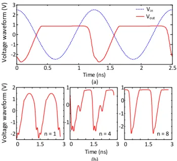
Taking the component availability into account, the NLTL will be made up of eight cells, composed by the inductance
L=0.3 nH and the varactor diode SMV1232, biased at 0 V. For fin sufficiently below fmax and nonlinear behavior of diodes, there should be a progressive compression of the wavefront. The results are analyzed in Fig. 2. In Fig. 2(a) a sinusoidal input at fin = 0.8 GHz with amplitude Ein = 2.5 V has been considered. The shockwave-like output waveform shows a significant falling–edge compression. For more insight, the waveform evolution through the various NLTL cells is represented in Fig. 2(b). In Fig, 3, the simulated waveform and output spectrum are compared with the measured ones. Discrepancies are attributed to parasitic effects in the hybrid circuit. Note that for comparison with the measurement results, the source impedance (having the original value Zc) is replaced with 50 Ohm. The NLTL is not matched in these conditions. However it should be matched when connected to the transistor output in the oscillator design.
0 0.5 1 1.5 2 2.5 -2 -1 0 1 2 3 V in Vout (a) Time (ns) Vo lta ge w av ef or m (V ) (b) -1 0 1 -2 -1 0 1 0 1.5 3 -2 -1 0 1 2 0 1.5 3 0 1.5 3 n = 1 n = 4 n = 8 Time (ns) Vo lta ge w av ef or m (V )
Fig. 2 NLTL with n = 8 and L = 0.3 nH. (a) Comparison between input and output voltage waveforms. (b) Waveform evolution though the NLTL cells. O ut put w av ef or m (V ) 0 1 2 3 4 5 -2.5 -2 -1.5 -1 -0.5 0 0.5 1 6 Time (ns) (a) 0 5 10 15 20 25 30 35 -60 -50 -40 -30 -20 -10 0 10 20 O ut put sp ec tr um (dB m ) (b) Frequency (GHz) Measuremet Measuremet Zs = 50 Ω Zs = Zc Simulation : Zs = 50 Ω Zs = Zc Simulation :
Fig. 3 Output signal of the NLTL. (a) Simulated and measured waveforms. The experimental waveform was obtained with the digital oscilloscope Agilent DSO90804A. (b) Spectra.
B. Wavefront-steepening oscillator
Due to the nonlinearity of the varactor diode, each NLTL section would ideally comprise the falling edge as T(Vh)–T(Vl) [11], where T V( )= LC VT( ), where CT is the total capacitance per NLTL section and Vh and Vl are the high and low levels. However, the maximum propagation frequency fmax will limit the minimum achievable transition time, which can be roughly
estimated from that of an RC low–pass filter, τ =r 0 35. / fmax [11, 28]. Therefore, fmax should be initially maximized using the method in Section II.A. The nonlinear behavior of the diodes prevents an a priori prediction of the required input amplitude. Therefore, a simulation of the line excited with a sinusoidal source and terminated with its approximate characteristic impedance Zc= L / Co must be carried out, as done in Section II.A. Next, a circuit capable to oscillate when loaded with the approximate NLTL characteristic impedance
c
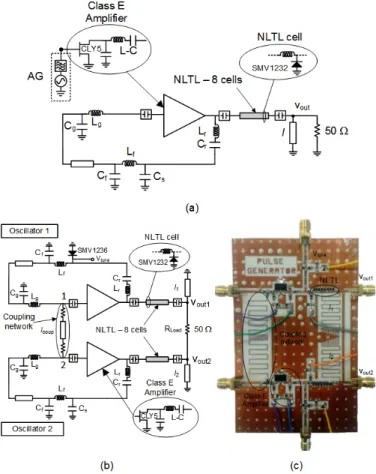
Z and providing the required excitation amplitude will be designed. The oscillation frequency must be the one considered in forced conditions, that is, fo = fin. In this case, we have chosen a Class-E oscillator topology, since the NLTL must be driven with sufficiently high amplitude to ensure the nonlinear operation of the diodes. The oscillator is composed by an amplifier with low output impedance [15] and a parallel feedback network to sustain the self–oscillation [Fig. 4(a)]. The transistor is a CLY5 biased at the gate voltage VGG = –1.5 V and the drain voltage VDD = 2.9 V. The use of an AG operating at the desired oscillation frequency, fAG = fo = 0.8
GHz, facilitates the large-signal oscillator design, due to the AG capability to force the frequency and oscillation amplitude at the fundamental frequency. To our knowledge, this AG method is the only one that allows imposing amplitude and frequency of the large-signal periodic oscillation, which should agree with the AG amplitude and frequency, then optimizing some circuit elements or parameters, so as to fulfill the non-perturbation condition (YAG = 0). Next, the oscillator load Zc is replaced with the NLTL. Its average input impedance should be similar, so the AG optimization should not have any difficulty to converge for an AG amplitude close to that of the previous design at the same frequency fAG = fo. It
might be convenient to further increase this amplitude to obtain the desired wavefront steepening effect. The amplitude is increased through a sweep, optimizing, for instance, the oscillator feedback elements at each sweep step, as has been done in this case. A pulsed waveform is obtained by connecting and tuning a high–impedance stub [Fig. 4(a)] to the output node through combination of reflection and delay effects. The length of this stub is easily tuned and due to its connection at the end of the NLTL, quite far from the active device, it has minimum impact on the fulfillment of the oscillation condition, or, equivalently, on the fulfillment of the AG non-perturbation condition. The resulting output voltage, named vout1(t), is shown in Fig. 7(a). However, there is little control on the pulse amplitude and width. For more flexibility, a design based on the coupling of two NLTL-based oscillators will be studied in the next section.
III. PULSE-SHAPING GENERATOR BASED ON TWO COUPLED OSCILLATORS
A. Proposed topology
The pulse shaping generator proposed here is based on the coupling of two NLTL oscillators [Fig. 4(b) and Fig. 4(c)]. Due to the low NLTL characteristic impedance, the output signal can be taken in a differential manner vout(t) = vout1(t) –
output nodes. The pulse shaping is carried out through two main actions: delay of vout2(t) with respect to vout1(t) (achieved by tuning one of the two coupled oscillators) and subtraction [through the differential extraction of the output signal vout(t)]. The individual pulses vout1(t) and vout2(t) can be equal or different. For instance, in the work [18] a slight variation of the length l of the output stub was carried out. However, in this work the transistor bias voltage is proposed, thus avoiding any changes in the original circuit layout. The varactor used to change the phase shift will be connected to the feedback network of the first oscillator [Fig. 4(b)]. The coupling network, connected to the gate terminals, will consist of a transmission line bounded with series resistances [29-32].
Fig. 4 NLTL-based coupled oscillator system. (a) Schematic of the individual oscillator. (b) Coupled oscillators. (c) Photograph.
Time (nsec)
1 3 5 7 9
500 mV/div
Fig. 5 Measured output signal of the sharpened–waveform oscillator terminated in 50 Ω.
The harmonic balance analysis of the coupled-oscillator system is involved due to the need of two auxiliary generators (AG1 and AG2) [25-26] in order to maintain the two circuits in an oscillatory stage, i.e., to avoid trivial solutions in which one of the oscillator circuits simply responds to the periodic solution generated at the other one without self-oscillating. Furthermore, the lack of symmetry gives rise to additional difficulties in the convergence process, since the AGs must be resolved in terms of their individual amplitudes and phase shift, on top of the common oscillation frequency (compare, for instance, with the case of push-push oscillators [33-34], where the phase shift is known beforehand and the amplitudes are equal). In view of these difficulties, a two stage methodology has been developed. In a first stage, the phase shift required between the two different oscillator elements is estimated through individual analysis of these elements in uncoupled conditions, with one waveform artificially delayed with respect to the other. In a second stage, a new reduced order formulation is used to obtain the bias voltage of the oscillator varactor that is required for the desired phase shift, as well as the synchronized oscillation frequency. The design steps are indicated in the flow chart of Fig. 6. The original oscillator must include the varactor diode that will be used at a later stage to change the phase shift between the oscillator elements. At Step 1, one parameter in one of the two oscillators (Osc2) is modified, so as to change the corresponding NLTL output waveform. The other oscillator design (Osc1) remains unchanged, with the AG (AG1) having the original steady-state variables and, therefore, fulfilling
YAG1 = 0. The second AG (AG2) is used as a forcing element (it does not fulfill the non-perturbation condition). It is connected to the transistor input terminal and enables a periodic forcing of the active sub-circuit and NLTL. It is also used to artificially shift the phase shift between the two oscillator circuits, operating at the same frequency. The tuning parameter (the transistor drain bias voltage, in this particular case) is varied, as well as the phase shift between the two AGs, until achieving the desired output pulse, extracted in a differential manner. If the AGs are connected at the input or near the input of the NLTL another possibility is to tune the AG amplitude (then, the tuning parameter would be optimized, instead of the AG amplitude, at the next step). At Step 2, the second oscillator is resolved isolated from the other. The AG amplitude (and possibly the transistor bias voltages) will have to be optimized to fulfill YAG2 = 0. This circuit level analysis is discussed in detail in Subsection III.B. At Step 3 (described in Subsection III.C), reduced-order models of the two individual oscillators, at their corresponding steady-state free-running oscillation points, are extracted through finite differences, using one AG, according to the methodology in [35]. The model of Osc1 must include the derivative with respect to the tuning voltage of the varactor diode, as this tuning voltage will enable the phase shift variation. The reduced-order models extracted in Step 4 are used to evaluate the phase shift variation versus the tuning voltage of the first oscillator element, as well as the oscillation frequency deviations resulting from this phase shift (Subsection III.C). The stability analysis is carried out with the reduced-order formulation in Section V, based on these
models. At Step 5, the result obtained with the reduced-order formulation is validated with a costly HB simulation of the two element coupled oscillator system. At this step, equivalent current noise sources at the coupling nodes should be extracted for each of the individual oscillators, simulated in uncoupled conditions, following the method in [36]. At Step 6, the noise models are introduced in the reduced-order formulation to obtain the phase-noise spectra, as described in Section VI.
1. Circuit level analysis with uncoupled oscillators: Osc1: Original design
Osc2: One parameter is tuned to vary the NLTL output waveform. AG2 operates in forcing mode.
Phase shift between oscillators is changed by varying φAG.
2. Circuit level:
Osc2 is solved to fulfill YAG2=0
3. Extraction of:
Reduced-order models of Osc1 and Osc2
Fourier coefficients of the individual NLTL output waveforms
6. Introduction of the noise models in the reduced-order formulation to
obtain the phase-noise spectra.
5. Extraction of equivalent current noise sources
Osc1 at resulting tuning voltage of varactor diode. Osc2 as in step 2.
4. Reduced order formulation.
Analysis of:
phase shift vs. tuning voltage oscillation and amplitude deviations.
Output waveform is estimated from the Fourier coefficients in Step 3. Stable range is determined.
Fig. 6 Flow-chart indicating the steps to be taken for the design of the coupled system of two NLTL-based oscillators.
B. Estimation of the phase shift between the oscillator elements
In a first stage, the two NLTL-based oscillators are analyzed in a separate manner, using an auxiliary generator per oscillator element. The corresponding AGs will have a phase shift φ , which is imposed by doing φAG1=0, φAG2 =φ. This
will give rise to a time shift between the individual output voltage waveforms, which will be used to estimate the differential output in coupled conditions. The drain bias voltage VDD of the active device is chosen to modify the waveform of the second oscillator (VDD2). Because the first oscillator operates exactly at the original conditions, only the second oscillator is actually analyzed. Its corresponding AG, connected to the gate terminal, is initially used just as forcing source at the original oscillation frequency, without fulfilling
YAG = 0. The time shift between the two waveforms is controlled with the phase φAG of the second oscillator. Note
that the preliminary analysis in our previous work [18]
involved a simulation of the NLTLs only, which prevented the use of tuning parameters affecting the active device, such as the drain bias voltage.
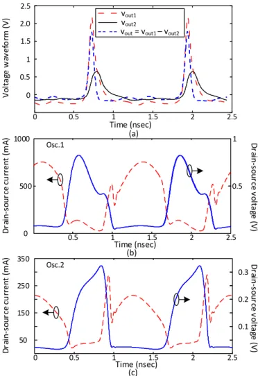
In a first application, the above methodology has been used to obtain a very narrow pulse through the mechanism illustrated in Fig. 7(a). The pulse vout1(t) is the one obtained through the design in Section II.B, by terminating the oscillator with a grounded parallel stub and biasing the transistor at VDD1 = 2.9 V. As observed in the figure, the rise time of vout1(t) is shorter than the decay time. A second pulse
vout2(t) of smaller amplitude is generated, by reducing the bias voltage VDD2 = 1.1 V of the second oscillator. When delayed as shown in Fig. 7(a), the second pulse is located under the slow decay section of vout1(t), so the differential signal vout(t) exhibits short rise and decay times. Once the desired waveform has been obtained, the AG frequency and amplitude of the second (modified) oscillator are optimized, so as to fulfill the AG non-perturbation condition YAG2 = 0. The results of this optimization, together with those corresponding to the original oscillator, will constitute the input data of the reduced-order model presented in Sub-section B. The drain voltage and current waveforms corresponding to each of the two coupled oscillators are shown in Fig. 7(b) and Fig. 7(c).
0 0.5 1 1.5 2 2.5 0 0.5 1 1.5 2.0 2.5 Vo lta ge w av ef or m (V ) Time (nsec) (a) vout1 vout2
vout = vout1 – vout2
50 150 250 350 0.1 0.2 0.3 0 0.5 1 1.5 2 2.5 Time (nsec) Dr ai n-so ur ce cu rr ent (m A) Dr ai n-s ou rce v ol ta ge (V ) 0.5 1 1.5 2 2.5 0 500 1000 0.5 1 Dr ai n-so ur ce cu rr ent (m A) Time (nsec) Dr ai n-s ou rce v ol ta ge (V ) (b) (c) Osc.1 Osc.2
Fig. 7 Differential extraction of pulsed waveforms using a forcing AG in one of the oscillator elements. (a) Pulse sharpening with the second oscillator biased at VDD2 = 1.1 V and phase shift φ = 15º (b).
VDD1 = 2.5 V and fundamental-frequency amplitude 2.88 V. (c) The
same for the second oscillator with VDD2 = 1.1 V and
fundamental-frequency amplitude 1.25 V. (a) (b) 0 1 2 3 4 5 -1 -0.5 0 0.5 1 1.5 2 Time (nsec) 0 1 2 3 4 5 -1 -0.5 0 0.5 1 1.5 Time (nsec) -1.5 Voltage waveform (V ) Voltage waveform (V )
vout = vout1 – vout2
Transmission line PFN [7]
Fig 8 Monocycle waveform. (a) Parameters: VDD2 = 2.5 V and
9.8º
φ= . (b) Switched polarity monocycle with parameters: VDD2 =
2.5 V and φ= −16º.
With pulses vout1(t) and vout2(t) of nearly identical amplitudes, and applying sufficient delay to avoid overlapping, a monocycle pulse vout(t) is obtained, as shown in Fig. 8(a). In that figure the second oscillator is biased at
VDD2 = 2.5 V and the phase shift is φ=9.8º. For comparison, the transmission-line pulse forming network used in the work [7] (which includes two carrier amplifiers and step-recovery diodes) has also been tested. When terminating one of the oscillators with that network, one obtains the lower amplitude monocycle shown in Fig. 8(a). By means of the proposed coupled system, the polarity of the monocycle can be electronically switched by simply varying the phase shift between the oscillator elements to φ= −16º [Fig. 8(b)].
The oscillator phase shifting will actually be carried by coupling the two oscillator elements, which will operate at the synchronized oscillation frequency ω. The coupled system will be analyzed with a new reduced-order formulation presented in the next sub-section.
C. Reduced-order model of the coupled-oscillator system
As already stated, the oscillators are coupled by means of a transmission line section, bounded by high resistors R [29-30], as shown in Fig. 4(b). The coupling network is connected to the gate nodes of the respective transistors, where the waveform is quasi-sinusoidal, so coupling effects can be assumed to be significant at the fundamental frequency only. Unlike [18], it is taken into account that due to changes in the second oscillator design or operation point, the oscillator characteristics will, in general, be different. For synchronization, the individual oscillation free-running frequencies, must, of course, be similar. However, the
individual amplitudes may be different to a larger extent. Assuming small coupling strength (high R value), the admittance function of each oscillator, of zero value in free-running conditions (Yk = 0), where k = 1, 2, can be described with a first-order Taylor series about the corresponding free-running solutions, of respective amplitude and frequency
,
ok ok
V ω . Note that the admittance function Yk is identical to
the AG current-to-voltage relationship. Through application of Kirchoff’s laws, the coupled system is governed by the following complex equations:
1 1 1 1 1 1 1 2 2 2 2 2 2 2 1 2 ( ) ( ) ( ) ( ) − + − + ∆ = − − − + − = − − j V o o e nb j j V o o nb e Y V V Y Y V Y V Y V e Y V V Y V e Y V Y V e φ ω η φ φ ω ω ω η ω ω (3)
where Vk (k = 1, 2) is the voltage amplitude of each oscillator circuit, once in coupled operation, and φ is the phase shift between the oscillator elements at the fundamental frequency. On the other hand, YVk,Yωk are the derivatives of the admittance functions, evaluated at the corresponding free-running points, with respect to the amplitude and frequency and Yη is the derivative of the first oscillator with respect to
the tuning parameter. The 2x2 admittance matrix of the symmetric coupling network has element values Y11 = Y22 = Ye and Y12 = Y21 = Ynb. In (3), it is taken into account that due to the autonomy of the coupled system the phase of one of the oscillator elements can be arbitrarily set to zero. The first oscillator is chosen here, so φ =1 0.
For each circuit, the derivatives are calculated in harmonic balance by means of an AG, introduced in parallel at the node where the coupling network will be connected (nodes 1 and 2, corresponding to the gate terminals in Fig. 4(b)). These calculations are carried out through finite differences, using the method described in [35-37]. The derivatives are obtained using an AG, with the pure HB system, including the whole harmonic content, as inner tier. For instance, to obtain the frequency derivative, the AG amplitude is fixed to VAG=Vok, performing a small sweep in ω about the free-running value AG
AG ok
ω =ω and obtaining the ratio between the admittance increment ∆YAG (calculated with HB) and the increment applied. The same procedure is applied for the calculation of the rest of derivatives. If the designer wishes to have a parameter available for consideration in the reduced-order model, the derivative calculation can be easily automated. For instance, the drain bias voltage VDD2 can be swept, obtaining for each VDD2, a set composed by the free-running solution
2, 2
o o
V ω (fulfilling the non-perturbation condition YAG =0), and the derivatives Yω2,YV2.
The nonlinear system in (3) can only be solved numerically, through an error minimization technique, which provides little insight into the coupled-system performance. For a better understanding of this system, it will be taken into account that, under weak coupling, a first order approximation can be carried out, which leads to the following complex equations:
2 1 1 1 1 1 1 1 2 2 2 2 2 2 j o V e nb o o j o V nb e o o V Y V Y Y Y Y e Y Y V V Y V Y Y e Y Y Y V φ ω η φ φ ω φ ω η ω − + + ∆ = − − + ∆ = + = − − + ∆ = (4)
where the following constant increments have been defined:
1 1 1 1 1 2 2 2 2 2 ∆ = + ∆ = + o V o o o V o o Y Y V Y Y Y V Y ω ω ω ω (5)
Two additional parameters will also be introduced:
2 1 1 1 2 2 o nb nb o o nb nb o V Y Y V V Y Y V = = (6)
With the aid of the above parameters, it will be possible to predict the behavior of a system of two coupled oscillators having different free-running amplitudes. Splitting (4) into real and imaginary parts and solving for the synchronization frequency ω, one obtains the expression:
2 2 2 2 V V Y Y Y Y φ ω ω= × × (7)
where the product means the following operation ,
Re( ) Im( ) Im( ) Re( ) sin a b
a b× = a b − a b = a b
α
and, ( ) ( )
a b angle b angle a
α = − . Performing this operation, the synchronized oscillation frequency ω is given by:
(
)
(
)
(
)
2 2, 2 2 2, 2 2 2, 2 2, sin sin( ) sin sin off V off nb V nb V V Y Y Yω ω Yω ω α φ α ω α α − + = − (8) where: 2 2 2, 2 2 2 2, 2 2 2 2, 2 2 ( ) ( ) ( ) ( ) ( ) ( ) off o e V off off V V nb nb V V V Y Y Y angle Y angle Y angle Y angle Y angle Y angle Y ω ω α α α = ∆ − = − = − = − (9)As gathered from (8), to first order, the oscillation frequency varies sinusoidally with the phase shift φ, with an offset depending on the original free-running point ∆Yo2 and
the parameter Ye of the 2x2 admittance matrix that describes
the coupling network. The oscillation frequency excursion depends on the magnitudes YV2,Yω2 that characterize the
second oscillator (the oscillator that does not contain the tuning element), the ratio between the free-running voltages
1/ 2
o o
V V and the coupling-network parameter Ynb. The parameter Ye gives rise to a constant pulling effect, whereas
synchronization is due to the signal of the first oscillator (the one tuned with the varactor diode), which affects the second oscillator through the parameter Ynb2.
Solving (4) for ∆η, an analytical expression is obtained for the tuning voltage of the first oscillator required for each φ value: 2 2 1 1 1, 1 1 2 2 1 1 2 2 2, 1 2 2 2 2 1 1 1 1 2 2 1 2 2 ( ) sin( ) ( )( ) ( ) sin( ) ( )( ) ( )( ) ( )( ) ( )( ) V V nb V nb V V V V nb V nb V V V V off V V off V V Y Y Y Y Y Y Y Y Y Y Y Y Y Y Y Y Y Y Y Y Y Y Y Y Y Y Y Y ω η ω ω η ω ω ω η ω η φ α φ α × ∆ = − + + × × × + − + + × × × × − × × × × (10)
The parameter ∆η affects the behavior of the two oscillators and, therefore, the phase shift φ between the two depends on the individual responses of these two oscillators. The coupled performance is actually described by the combination of (8) and (10). Interestingly, in case the free-running oscillators are equal, the tuning parameter ∆η required for each φ will not depend (to first order) on the frequency derivative Yω1=Yω2 .
Provided that the amplitude increments remain small, it will be possible to reuse the Fourier harmonic coefficients of the original output-pulse waveforms (V1m,V2m) for an estimation
of the differential output. After an initial storage of these Fourier coefficients, the output pulse can be approached as:
( ) 1 2 ( ) jm t jm t pulse m m m k v t =
∑
V e ω −∑
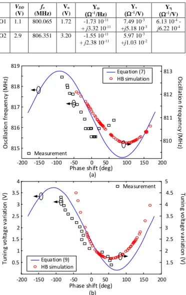
V e ω φ+ (11) where it is taken into account that the two oscillators operate at the same synchronized frequency ω, with the phase shift φ. Note that in case variations in the design parameter (VDD2 for instance) are considered, use of (11) will require an additional storage of the Fourier components V2m, corresponding to each parameter value.The practical application of expressions (8) and (10) is shown in the following. The drain bias voltage, oscillation frequency, amplitude and derivatives obtained with the method described in Section III.B are shown in Table I. Note that only the design of the second oscillator is modified. Fig. 9 compares the results obtained with (8) and (10), and with a costly HB simulation of the coupled system at circuit level. In Fig. 9(a) the synchronized oscillation frequency is traced versus the phase shift φ and Fig. 9(b) presents the tuning voltage required for each φ value. Note that HB convergence was not possible in the whole φ interval (-180º, 180º). Furthermore, the more discrepant HB points in Fig. 9 were obtained with rather high convergence errors.
The sketch and picture of the measurement set-up are shown in Fig. 10. It is based on the use of the Agilent DSO090804A Digital Storage Oscilloscope and the spectrum analyzer Agilent E4446A (with phase noise measurement personality). Connecting the two individual oscillator outputs to two power splitters, we can alternatively measure the differential output waveform, the individual oscillator waveforms and the individual oscillator spectra. Experimental measurements are superimposed in Fig. 9. These measurements are only possible
in the stable phase shift range, which will be analyzed in the next section. The experimental range was (–90º, 55º). We must emphasize that the new relationships (8) and (10) have a general validity to predict the coupled behavior of any two different oscillators with similar oscillation frequencies.
TABLEI VDD (V) fo (MHz) Vo (V) Yω (Ω−1/Hz) Yv (Ω−1/V) (ΩY−1η /V) O1 1.1 800.065 1.72 -1.73 10-11 + j3.32 10-11 7.49 10-3 +j5.18 10-3 6.13 10-4 - j6.22 10-4 O2 2.9 806.351 3.20 -1.55 10-11 + j2.38 10-11 5.97 10-3 +j1.03 10-2 815 816 817 818 819 -200 -150 -100 -50 0 50 100 150 200
Phase shift (deg)
O sc ill at io n f re que nc y (MH z) 0.5 1 1.5 2 2.5 3 3.5 4 810 811 812 813 HB simulation Equation (7) -200 -150 -100 -50 0 50 100 150 200
Phase shift (deg)
1.5 2 2.5 3 3.5 4 4.5 5 HB simulation Equation (9) Tu nin g vo ltag e v ar ia tio n (V ) Tu nin g v olt ag e v ar ia tio n ( V) O scil lat io n f re que nc y (MH z) (a) (b) Measurement Measurement
Fig. 9 Coupled system of two oscillators biased at VDD1 = 2.9 V and
VDD2 = 1.1 V. (a) Oscillation frequency variation versus the phase
shift, obtained with (8) and with HB. Measurements in the stable range are superimposed. (b) Tuning voltage variation versus the phase shift using (10) and HB. Measurements are superimposed.
Fig. 10 Measurement test-bench. (a) Sketch. (b) Photograph.
1 3 5 7 9 0 0.5 1 1.5 2 2.5
Differential output voltage waveform
(V ) Time (nsec) (a) 1 3 5 7 9 500 mV/div (b) Time (nsec) HB simulation Prediction with (10)
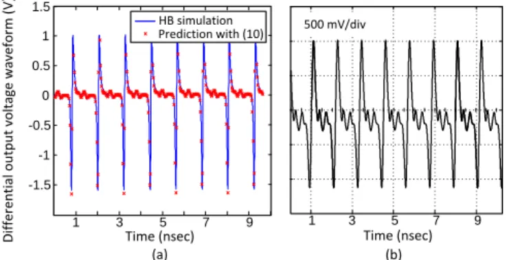
Fig. 11 Pulsed waveform obtained for VDD2 = 1.1 V and φ =15º. (a)
HB simulation and prediction with (11). (b) Measured waveform.
-0.5 0 0.5 1 1.5 1 3 5 7 9 Time (nsec) (a) 1 3 5 7 9 Time (nsec) (b) 500 mV/div
Differential output voltage waveform
(V
)
HB simulation Prediction with (10)
Fig. 12 Monocycle waveform obtained for VDD2 = 2.5 V and 9.8º
φ = . (a) HB simulation and prediction with (11). (b) Measurement.
-1.5 -1 -0.5 0 0.5 1 1.5 1 3 5 7 9 Time (nsec) (a) HB simulation Prediction with (10) 1 3 5 7 9 Time (nsec) (b) 500 mV/div
Differential output voltage waveform
(V
)
Fig. 13 Switched polarity monocycle obtained for VDD2 = 2.5 V and 16º
φ = − . (a) HB simulation and prediction with (11). (b)
Measurement.
The narrowest output pulse is obtained for the phase shift 15º
φ= . From (10), the required tuning voltage is 0.93
∆η = V. The differential waveform obtained with HB and with the approach (11) is shown in Fig. 11(a). The measured waveform can be seen in Fig. 11(b), where several cycles are presented to show that there is no modulational instability, leading to a self-induced modulation of the waveform [9]. Discrepancies are attributed to parasitics in the hybrid NLTL. Note that most published circuits achieving very narrow pulses at high fundamental frequency are based on driven NLTLs implemented on MMIC technology, for instance [2],[10,11]. We did not aim at obtaining comparable results due to the limitations in the hybrid technology used, mostly coming from the parasitics in the packaged varactor diodes. An analogous approach has been applied to obtain a monocycle pulse. An optimized waveform is obtained for
VDD2 = 2.5 V and φ=9.8º, obtained with ∆ =η 1.3 V. The simulated and measured waveforms are presented in Fig. 12. The polarity of the monocycle can be inversed by simply changing the phase shift from 9.8° to –16° (∆ =η 1.82 V), as shown in Fig. 13. Therefore, the polarity of the monocycle can be switched electronically in a very simple manner.
IV. STABILITY ANALYSIS OF THE COUPLED-OSCILLATOR SYSTEM
In a first stage, stability of the two individual oscillators, with different VDD values, is analyzed at circuit level, using pole-zero identification [21-22]. In a second stage, the stability of the coupled system is evaluated through a perturbation analysis of this system. Because the two oscillators must be individually stable, instability may only arise from the coupling effects. On the other hand, due to the similarity in the individual free-running frequencies and the weak coupling conditions, instability (obtained in a certain phase shift range) should be due to real poles or complex-conjugate poles σ ± jΩ with low frequency Ω, in the order of the difference between the free-running frequencies [25-26]. Both types of dominant poles should be detectable with the reduced-order formulation. For the stability analysis of the coupled system, a small instantaneous perturbation is considered, which will gives rise to the following increments of the state variables:
1 01 1 1 2 02 2 2 1 1 2 2 2 ( ) ( ), ( ) ( ), ( ) 0 ( ), ( ) ( ), = + ∆ + = + ∆ + = + = + V t V V V t V t V V V t t t t t δ δ φ δφ φ φ δφ (12)
Next, Kirchoff’s laws are applied to the perturbed system. When doing so, the exponentials of the phase variables are approached as:
(
)
( ) 1 ( ) i i j t j i eφ eφ + jδφ t (13)It is also taken into account that the complex-frequency increment gives rise to a time-derivative operator [29-32], so the perturbed system can be written:
1 1 1 1 1 1 1 1 1 2 1 1 2 1 1 1 1 1 1 1 1 1 2 1 1 2 2 2 2 2 2 2 2 2 1 2 2 1 2 2 2 2 2 2 2 2 2 1 2 2 1 2 r r r r i V i i i i r V r r r r i V i i i i r V V a a Y V Y Y V V a a Y V Y Y V V a a Y V Y Y V V a a Y V Y Y V ω ω ω ω ω ω ω ω φ φ φ φ φ φ φ φ φ φ φ φ φ φ φ φ φ φ φ φ ∆ ∂ ∂ ∆ + ∆ + = ∆ + ∆ ∂ ∂ ∆ ∂ ∂ ∆ + ∆ − = ∆ + ∆ ∂ ∂ ∆ ∂ ∂ ∆ + ∆ + = ∆ + ∆ ∂ ∂ ∆ ∂ ∂ ∆ + ∆ − = ∆ + ∆ ∂ ∂ (14)
where superindexes r and i indicate real and imaginary parts and the following functions have been defined
2 1 ( ) 1 1 j nb a = −Y e φ φ− and (1 2) 2 2 j nb a = −Y e φ φ− . By grouping terms, one obtains the following LTI system, in matrix form:
[ ]
[ ] [ ] [ ]
1 1 1 2 2 1 2 1 1 2 2 ; V V V V M M M M φ φ φ φ − ∆ ∆ ∆ ∆ = = ∆ ∆ ∆ ∆ (15)where the matrixes [M1] and [M2] are given by:
[ ]
[ ]
1 1 1 1 1 1 1 2 2 2 2 2 2 1 1 1 1 2 1 1 1 1 2 2 2 2 2 1 2 2 2 2 1 2 0 0 0 0 0 0 0 0 0 0 0 0 i r r i i r r i r r r V i i i V r r r V i i i V Y Y V Y Y V M Y Y V Y Y V a a Y a a Y M a a Y a a Y ω ω ω ω ω ω ω ω φ φ φ φ φ φ φ φ − = − ∂ ∂ − ∂ ∂ ∂ ∂ − ∂ ∂ = ∂ ∂ − ∂ ∂ ∂ ∂ − ∂ ∂ (16)Note that the phase derivatives must be particularized to each steady-state solution, given by φ1=0, φ2=φ. This
provides: 1 1 1 1 1 2 2 2 2 2 1 2 ; ; − − ∂ ∂ = = − ∂ ∂ ∂ ∂ = − = ∂ ∂ j j nb nb j j nb nb a a jY e jY e a a jY e jY e φ φ φ φ φ φ φ φ (17)
The stability is determined by the eigenvalues of the matrix [M] in (15). Due to the autonomous behaviour of the coupled-system, one of these eigenvalues must necessarily be equal to zero for all the φ values. Mathematically this comes from the fact that the last two columns (c3, c4) of the matrix [M], containing the phase derivatives, are linearly related, as
3 4 0
c +c = . The stability properties will be determined by the remaining three eigenvalues.
For more insight into the stability properties of the coupled system, an approximation will be carried out next. When assuming oscillator admittance functions of the form
( , ) r( ) i( )
Y V ω =Y V + jY ω and neglecting the amplitude variations ∆ ≅ , system (14) reduces to: V 0
1 1 1 2 1 1 1 1 2 2 2 2 1 2 2 2 1 1 1 1 1 1 2 2 2 2 2 2 1 1 1 1
cos sin cos sin
cos sin cos sin
∂ ∂ ∂ ∂ ∆ ∆ = = ∆ ∂ ∂ ∆ ∂ ∂ − − + ∆ = − − + i i i i i i i i r i r i nb nb nb nb i i r i r i nb nb nb nb i i a a Y Y a a Y Y Y Y Y Y Y Y Y Y Y Y Y Y ω ω ω ω ω ω ω ω φ φ φ φ φ φ φ φ φ φ φ φ φ φ φ φ 1 2 ∆ φ φ (18)
The stability properties of this approximate system will be determined by the two eigenvalues of the matrix in (18), given by the roots of the following second-order polynomial:
2 2 2 1 1
2 1
cos sin cos sin
0 r i r i nb nb nb nb i i Y Y Y Y Yω Yω φ φ φ φ λ − + + − λ= (19)
One of the roots of this polynomial is λ1=0, in agreement with the autonomy of the coupled system. The second root is:
2 2 1 1
2
2 1
cos sin cos sin
r i r i nb nb nb nb i i Y Y Y Y Yω Yω φ φ φ φ λ = + + − (20)
For stability, the above eigenvalue must be negative. Qualitative changes of stability, or bifurcations [25-26, 37], will occur at the phase values leading toλ2=0. These phase values fulfil: 2 1 2 1 2 1 2 1 cos sin 0 r r i i nb nb nb nb i i i i Y Y Y Y Yω Yω φ Yω Yω φ + + − = (21)
It is derived in a straightforward manner that the two solutions of (21) can be written as φ φ1b, 180ºb2 =φ1b+ , so the approach predicts a stable range of 180º , regardless of the
particular oscillator characteristics. With different oscillators, the stability boundaries will be located at unsymmetrical phase shift values φb1, φb2. For identical oscillators, the above
expression would provide the stability boundaries
1,2 90º
b
φ = ± . Another relevant conclusion derived from the approximate expression (20) is that in case the frequency derivative of one of the oscillators is much smaller than the other, the pole λ will be mostly influenced by the properties 2
of the corresponding oscillator (assuming not too different values of Ynb1, Ynb2).
The analysis above has been applied to the two different designs of the previous section. The circuit level stability analysis of the two individual oscillators (based on pole-zero identification) demonstrates stable behaviour. Next, the stability of the coupled system is analysed using (15). In Fig. 14(a), the four real poles provided by this system have been traced versus the phase shift φ. As expected, the real pole associated with the system autonomy γ1=0 remains at zero
for all the phase shift values. The next dominant real pole γ 2
is due to the coupling effect. This is compared with the prediction by the approximate expression (20), traced in dotted line. The stable phase shift interval obtained using (15) is delimited by φb1= −107º , 73ºφb2= . The addition of the two
values is 180º, in agreement with the prediction of (20). In the measurements, the stable interval was (–95º,55º), as shown in Fig. 9.
As seen in Fig. 14, there are two additional real poles
3, 4
γ γ , relatively far from the imaginary axis, that exhibit very small variation with the phase shift φ. These two poles have their origin in the dominant real poles of the two individual free-running oscillators, prior to their connection to the coupled system. As demonstrated in [26, 38], the dominant real pole γ of a free-running oscillator has the approximate value:
(
)
2 V o Y Y V Y ω ω σ = − × (22)which depends on the amplitude and frequency derivatives of the admittance function of that oscillator Y Y VV, ω, o, as well as
the oscillation amplitude Vo. For the two individual free-running oscillators, one obtains the values
8 1 8 1
1 5.5 10 s , 2 9.08 10 s
o o
γ
= − −γ
= − −, which approximately correspond to those of the real poles γ γ . In the case of two 3, 4 equal oscillators, the free-running poles will be identical
1 2
o o
γ = γ and they are likely to evolve into a pair of complex-conjugate poles when the two oscillators are coupled.
-8 -7 -6 -5 -4 -3 -2 -1 0 1 2 -0.8 -0.6 -0.4 -0.2 0 0.2 0.4 0.6 0.8 1 Im ag in ar y (G Hz ) Real (MHz) -8 -6 -4 -2 0 2 -200 -150 -100 -50 0 50 100 150 200
Phase shift φ (deg)
Re al p ar t ( × 10 8 ) (a) (b) Equation (19) System (14) γ3 γ4 γ1 γ2 -100 -50 0 50 -0.2 0 0.4 0.2
Fig. 14 Stability analysis of the coupled-oscillator system providing a narrow pulse. (a) Analysis versus the phase shift based on (15), with the result of the approximate expression (20) for λ superimposed. 2 (b) Results of pole-zero identification at circuit level for the particular phase shift value φ =15º.
Due to the HB convergence difficulties of the coupled-system, the rigorous stability analysis of this system has only been carried out for the particular phase shifts that provide the narrow pulse and the monocycle pulse, obtaining stable behaviour in the two cases. The pole locus obtained through pole-zero identification (at circuit level) in the case of the narrow pulse, is shown in Fig. 14(b). In total agreement with the reduced-order model, this pole locus shows the presence of four real poles, or four complex-conjugate poles at the fundamental oscillation frequency ω of the coupled system. Note that due to the relationship between Floquet multipliers and poles [39], a pair of complex conjugate poles at the fundamental frequency σ± jω is equivalent to a real pole σ , as both this complex-conjugate poles and the real pole are associated to a same Floquet multiplier. This is why the four real poles in the analysis of Fig. 14(a) appear as four complex-conjugate poles at the oscillation frequency ω in the analysis of Fig. 14(b). Pole-zero identification [21-12] was initially carried out in a broadband where no unstable poles were found. This is in agreement with the fact that the weak coupling of two oscillators at similar frequencies should only give rise to either real poles or poles with small beat frequency Ω. The detailed identification in Fig. 14(b) has been carried out about the oscillation frequency, where it is generally more accurate than at baseband.
V. PHASE NOISE OF THE COUPLED-OSCILLATOR SYSTEM In a manner similar to the stability analysis, the phase noise of the coupled oscillator system will be investigated through the combination of a detailed analysis based on circuit-level simulations and a new reduced-order formulation. Once the phase-noise spectrum of each individual oscillator has been obtained at circuit level, using the conversion matrix approach [40-41], an equivalent noise source, located at the node where each oscillator will be connected to the coupling network, is fitted until obtaining a similar phase noise spectrum, following the technique proposed in [36]. For simplicity and better insight, only white-noise sources will be taken into account in the reduced-order formulation. The consideration of flicker noise in the reduced-order analysis would require an additional baseband equation [26]. The analysis would be based on a formulation of the perturbed system about dc and the fundamental frequency, and the model extraction would require the use of auxiliary generators at dc and the fundamental frequency, applying a finite-difference technique [35] to obtain derivatives with respect to the dc voltage and the fundamental amplitude and frequency. Departing from the perturbed system in (14), in the presence of the two equivalent noise sources, the coupled system will be ruled by the following equations:
[ ]
[ ]
1 1 1 1 1 1 2 2 1 2 1 1 2 2 2 2 2 2 ( ) ( ) ( ) ( ) r n o i n o r n o i n o I t V V I t V V V V M M I t V I t V φ φ φ φ ∆ ∆ ∆ ∆ − = ∆ ∆ ∆ ∆ (23)where the phase derivatives are evaluated at φ1=0, φ2=φ
using expressions (17) and Ink( )t , with k = 1, 2, are the equivalent current noise perturbations. The phase-noise spectrum is obtained through application of the Fourier transform to the above system, taking into account that the two noise sources are uncorrelated and so are the real and imaginary parts of each of these two noise sources [38, 40-41]. This provides the following noise spectra:
[
]
{
[
]
}
2 1 2 2 2 1 2 2 1 1 V V ( ) ( ) ( ) ( ) ( ) N (Ω)N (Ω) ( ) n n V V diag M j M j φ φ + − + − ∆ Ω ∆ Ω = ∆ Ω ∆ Ω = Ω Ω (24)where N (Ω) is directly derived from the right hand vector in V (23) and the conversion matrix
[
Mn(jΩ)]
is given by:In order to get an intuitive understanding of the noise behaviour of the two coupled oscillators, we will proceed in a manner similar to what was done in the stability analysis, that is, assuming admittance functions of the form
( , ) r( ) i( )
Y V
ω
=Y V + jYω
and neglecting the amplitudevariations ∆ ≅ . This simplification leads to the following V 0 2x2 conversion matrix: 1 1 1 1 2 2 2 2 1 2 1 1 1 1 2 2 2 2 1 2 ( , ) i i i i i i i i i i i i a a j Y MC a a j Y a a j Y a a j Y ω ω ω ω φ φ φ φ φ φ φ φ φ ∂ ∂ Ω − − ∂ ∂ Ω = = ∂ ∂ − Ω − ∂ ∂ ∂ ∂ Ω − − ∂ ∂ = ∂ ∂ − Ω − ∂ ∂ (26)
where the phase derivatives are evaluated at φ1=0,φ2 =φ. By
means of a derivation analogous to the one in (24), one obtains the following analytical expression for the phase noise spectral density of the first coupled oscillator:
2 2 2 2 2 1 2 1 2 2 2 2 1 2 4 2 2 2 1 1 2 1 2 2 1 ( ) ( ) ∂ ∂ ∂ + Ω +∂ ∆ = ∂ ∂ Ω + Ω ∂ + ∂ i i i i i i i i i a a Y N N a a Y Y Y Y ω ω ω ω ω φ φ φ φ φ (27)
where two functions have been introduced:
2 2 1 2 1 2 2 2 1 2 2 2 , n n o o I I N N V V = = (28)
Calculation of the phase derivatives in (27) from (17) provides an explicit relationship between the phase-noise spectral density and the phase shift φ :
(
)
(
)
2 2 2 2 1 1 2 2 1 2 2 2 2 1 1 2 2 2 1 1 1 2 2 2 2 1 cos ( , ) sin ( , ) ( ) sin 2 ( , ) ( ) ( , ) + ∆ = + Ω + + Ω − + Ω Ω + Ω r r nb nb i i nb nb r i r i nb nb nb nb i Y N Y N D Y N Y N D Y Y N Y Y N D Y N D ω φ φ φ φ φ φ φ φ (29)where the denominator is given by:
(
)
4 2 1 2 2 2 1 2 2 1 1 2 2 1 ( , ) ( ) ( ) cos ( ) sin ) i i i r i r i i i i nb nb nb nb D Y Y Y Y Y Y Y Y Y Y ω ω ω ω ω ω φ φ φ Ω = Ω + +Ω + + − (30)The expression for 2 2( )
∆φ Ω is identical, with the subindexes 1 and 2 interchanged. As expected, due to the autonomy of the coupled system, there is a common factor Ω2 in the denominator. On the other hand, the two individual expressions for the phase-noise spectral density, 2
1( )
∆ Ωφ
and ∆φ2( )Ω 2 become equal to those corresponding to the
individual free-running phase-noise spectra for Ynb1 = Ynb2 = 0,
that is, when the two oscillators are not coupled. These individual phase noise spectra are given by:
2 1 2 2 1 2 2 2 2 2 1 2 ( ) ; ( ) i i N N Yω Yω φ φ ∆ Ω = ∆ Ω = Ω Ω (31)
At low frequency offset Ω, the constant term will dominate in the numerator and the Ω2 term will dominate in the denominator. Therefore, the spectrum will exhibit the –20 dB/dec decay that is typical of an autonomous system under the influence of white-noise sources only. From inspection of (29) and (30), at low offset frequency the phase-noise spectrum will be the same for the two oscillator elements. Due to the term in sin( )φ in the denominator, at constant offset frequency, the variation of the phase-noise spectral density will not be symmetrical about φ=0, unless the two oscillators are identical. At phase shift φ = 0º, the phase-noise spectral density is given by:
(
2 2)
2 2 2 1 1 2 2 1 2 1 4 2 2 2 1 2 1 2 2 1 ( ) ( ) ( ) + + Ω ∆ = Ω + Ω + r r i nb nb i i i r i r nb nb Y N Y N Y N Y Y Y Y Y Y ω ω ω ω ω φ (32)Comparing with (31) and assuming approximately equal noise sources and oscillation amplitudes, the phase noise spectrum of the two coupled oscillators will be smaller than those of the individual oscillators by the following amount:
2 , 2 , ( ) 10 log10 ( ) = Σ i k red i k Y S Y ω ω (33)
where k =1, 2. Note that the above expression is valid for φ = 0º, at low frequency offset. From (33), the phase noise spectrum will be better than that of any of the two individual oscillators. Expression (33) predicts an improvement of about 3 dB in the case of two equal oscillators. In the unlikely case of two oscillators with very different phase noise levels, the response of the coupled system will approach the better one, in agreement with physical intuition.
Coming back to the general expression (29), (30), another interesting fact is that the denominator takes a minimum value at the stability boundaries, determined by the condition (21). At these boundaries the term in brackets affecting Ω2 in the
denominator vanishes and this denominator takes the value
2 2 4
1 2
i i b
D =Yω Yω Ω . On the other hand, the minimum phase